1. Introduction
The world’s energy is going through a transformation from being heavily reliant on fossil fuels to being reliant on renewable resources. Furthermore, renewable energy has been targeted in the quest to delay or even stop the major challenges of climate change and global warming [
1]. The world’s photovoltaic installed capacity steadily grew from 135 GW in 2013 to 480 GW by the end of 2018, rising 3.5-fold over five years.
With the development of solar cell structure design, micro-nano laser precision machining, and other technologies, the cost per kilowatt of photovoltaic power generation has decreased [
2]. However, one key concern that remains unresolved in the PV industry is the degradation of field-installed modules.
According to King [
3], field modules undergo regular temperature swings of around 60 °C (maximum). Temperature fluctuations result in the initiation and progression of fatigue cracks in the solder interconnection. This is caused by a mismatch in the thermal expansion coefficients (CTE) of silicon, glass, copper and solder when they are bonded together. There are two types of CTE mismatches: local and global. Clech [
4] clarified that when solder joints are stressed and deformed to accommodate the effect of CTE mismatch from surrounding component materials such as cells, glass and interconnect, global CTE mismatch occurs. In addition, local CTE mismatch occurs when the solder material’s expansion is limited by the material to which it is soldered. The development of microcracks is one of the results of solder joint deterioration. An open circuit will result if a crack spreads across the entire joint region. An open circuit increases the electrical resistance across the solder joint. As a result, this phenomenon has a substantial effect on the production capacity of c-Si solar PV modules (PVMs). Since power loss is linked to increasing series resistance (Rs) in the form I
2R
s [
5,
6], high-current PV modules are particularly affected.
When the temperature of the solder rises, it creeps. At high homogeneous temperatures, such as those found in tropical climates [
7], the creep response is important. Grain boundary sliding (GBS) and matrix creep (MC) are two factors that contribute to solder creep. It has been discovered that the latter has a more destructive creep function, resulting in a shorter joint life. Clech [
4] further indicated that the creep mechanism is temperature- and stress-dependent and that it increases as the strain rate/deformation increases. The formation of a brittle intermetallic compound (IMC) layer in c-Si PVMs is a result of a soldered tin-containing interconnection. On one side, the IMC layer is formed between the solder and the copper ribbon interface, and, on the other side, it is formed between the solder and the silver fingers. Cu
3Sn
5 or Ag
3Sn grains suspended in a solder matrix make up the IMC. The resulting thermo-mechanical stress causes a change in the microstructure of the IMC layer in the solder joint during thermal cycling of the PV module (coarsening and thickening). As a result, this layer is vulnerable to crack initiation and propagation. For high-temperature operations, this effect is important.
Research into solar PV reliability is continuous, with several reported studies, such as in [
8,
9,
10,
11,
12,
13,
14,
15,
16,
17,
18]. However, some of the shortcomings identified include the over-simplification of the constitutive behaviors of the constituent materials forming the solar cell as well as the non-inclusion of intermetallic compound (IMC) layers in solder interconnect geometry. In their thermo-mechanical assessment of encapsulated solar cells, Dietrich et al. [
11] modeled the solder interconnection as “interconnection paste,” ignoring the existence of IMCs. Similarly, Wiese et al. [
12,
13], in investigating the constitutive behavior of copper ribbons, modeled silicon and silver materials in the cell as linear elastic in addition to ignoring the presence of IMCs. Furthermore, Chen et al. [
14] investigated the residual stress and bow induced by soldering in the silicon cell interconnect by modeling all cell materials as temperature-independent elastic, perfectly plastic. Eitner et al. [
16,
17], in the investigation of thermal stresses and strains in solar cells, and Hasan et al. [
8,
18], in the finite element analysis and life prediction of solar PV modules, used material constitutive models derived from experimental testing that accurately describe the true mechanical properties of various solar cell materials. However, the model used in their investigation did not include a solder with its IMCs. In the case of Hasan et al. [
8,
18], the model was simplified further to exclude solder interconnection. On the other hand, Zarmai et al. [
19] performed an optimization study on solder interconnects in PV modules using the Taguchi method. The Cu3Sn5 IMC layer was included in the geometric model used for the analysis, but the Ag3Sn IMC layer was not. Furthermore, except for the solder, which showed creep, the study used linear elastic models to predict the constitutive behavior of all laminating materials.
The absence of IMCs in these experiments, according to the studies examined, may result in inaccurate simulation results. For tin-based solder alloys and metallized copper bond pads, IMC formation in solder joint interfaces is well-known. Another reason that researchers avoid using IMCs in simulations is the large number of mesh elements and nodes produced, which necessitates the use of a high-performance computer (HPC) for a numerical solution. HPCs with superior processing power and material property data are now available for the IMCs, thanks to recent technical developments and materials engineering studies. The over-simplification of material behavior and cell geometry has led to discrepancies in reported modeling results. In addition, for thermal cycling research, most modeling studies used the International Electrotechnical Commission qualification test standard (IEC 61215) conditions. The PV modules’ real field module temperature cycles (which are location-dependent) receive very little attention.
All constituent materials, as well as the solder and its derivative IMC layers, were included in the three-dimensional geometric models of the c-Si solar cell (cell-to-cell interconnection) in this study. The thermo-mechanical response of the cell to field temperature cycles created from in-situ climatic conditions in a Sub-Saharan Africa environment (Kumasi, Ghana) was then simulated using a finite element analysis (FEA) program (ANSYS v 18.2). Furthermore, the creep damage in solder joints for both Sn60Pb40 and Sn3.8Ag0.7Cu alloys was analyzed using simulation results from field temperature cycles.
2. Materials and Methodology
2.1. Test Rig for Data Collection and Generation of Test Region Thermal Cycle Profile
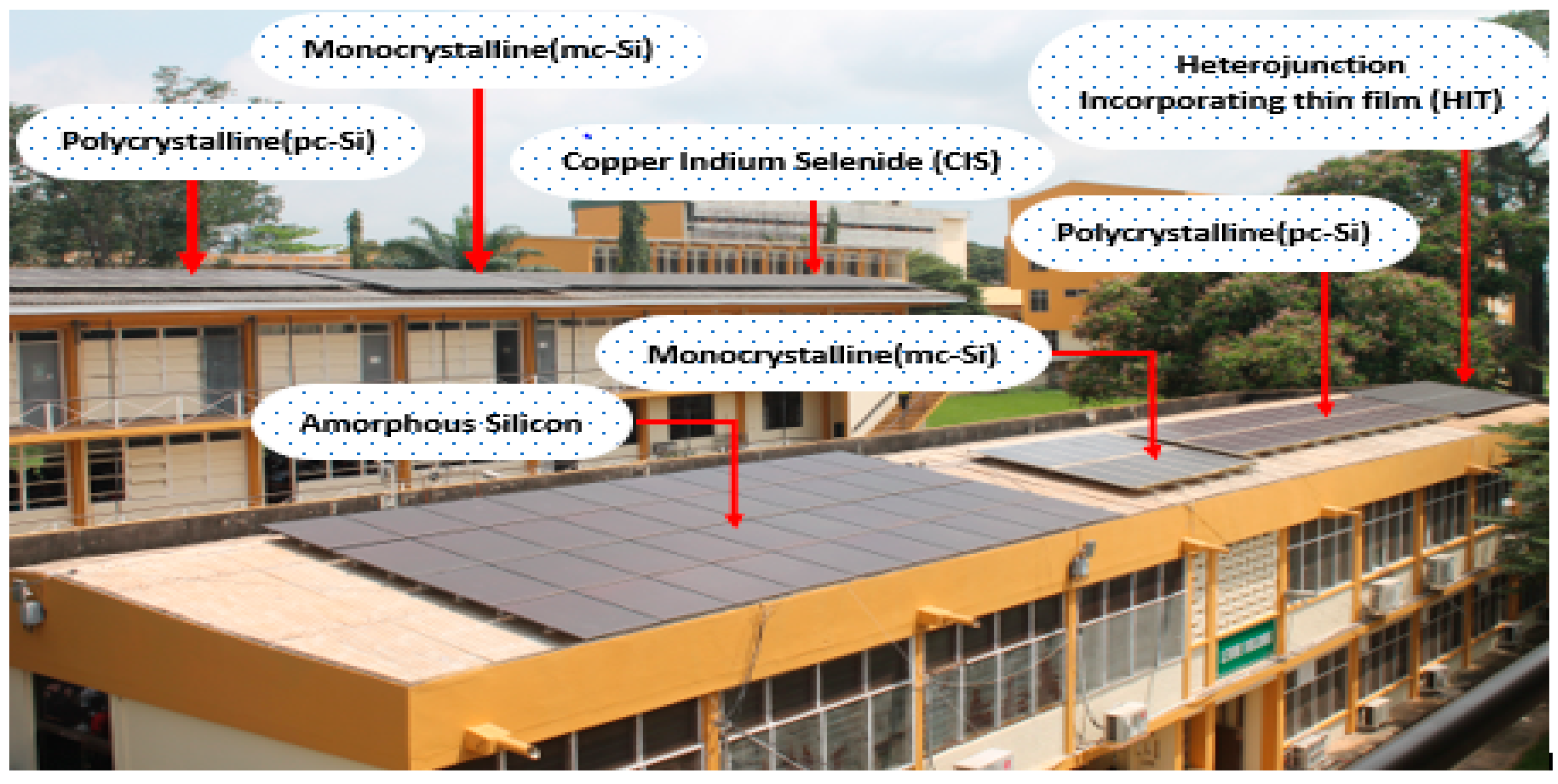
Figure 1 shows the rig for monitoring the outdoor climate used for this study. The rig contains other types of crystalline silicon PV modules. However, only the mono-crystalline modules were used for this investigation.
Figure 2 presents the monitoring station that was used for the data collection. The rigs are located at the College of Engineering KNUST, Kumasi, Ghana. The system was installed in 2012 with financial assistance from the World Bank through the Africa Renewable Energy Access programme (AFREA) under the project title, Capacity Upgrading for West African Partners in Renewable Energy Education. The site location (College of Engineering, KNUST, Kumasi, Ghana) is latitude 6°40″ N and longitude 1°37″ W, at an elevation of 250 m above sea level.
The modules are unshaded and mounted on an inclined rooftop with a tilt angle of 5°, and oriented toward the equator (southwards). Furthermore, a 4 kW Sunny Boy DC-AC inverter (SB 3800), manufactured by System, Mess and Anlagentechnik (SMA) in Niestetal, Germany connects each of the various PV module technologies to the grid. There are five inverters connected and integrated to communicate with a SMA Sunny WebBox via a Bluetooth ad-hoc connection. The SMA Sunny WebBox transmitted and stored the data output from the PV systems on a dedicated server. Additionally, an SMA Sunny portal was created on the dedicated server from the University network to provide an online monitoring system. Calibrated platinum sensors (PT100) manufactured by TC Limited in Uxbridge, United Kingdom with measurement accuracy of ±0.5 °C, resolution of 0.1 °C positioned at the center of each module (on the backside) measured the module temperatures. The data logged include environment temperature, total insolation, module temperature, operating current and voltage, wind speed and total output power.
The data were collected at 5-min intervals between the periods of March 2012 and December 2014. The study and data analysis were limited to the mono-crystalline PV-modules.
The study used four temperature load profiles (2012, 2013 and 2014) and test region average (TRA) thermal cycles created from three years of real-time monitoring of installed PV modules at the test site. In a previous study [
20], the methodology for producing these temperature profiles was extensively discussed.
2.2. Thermal Loads and Boundary Conditions
Figure 3 and
Table 1 summarize the results of temperature cycle profiles generated from the real time outdoor weathering of the PV modules. The profiles show extended dwell times as well as overall cycle time. A typical daily cycle time is completed in 86,400 s (24 h).
As shown in
Table 1, the mean daily temperature gradients for the generated cycles are relatively smaller when compared with the IEC 61215. A maximum of 40.2 °C was recorded in 2012, whereas the IEC 61215 temperature gradient is 125 °C.
The summary of the critical parameters presented in
Table 1 shows that the effect of the employment of IEC 61215 on the thermo-mechanical degradation qualification of the c-Si PV module is likely to be significantly different from the generated temperature cycles.
2.3. Solar Cell Materials and Properties
Figure 4 presents the architecture of a conventional c-Si PV cell interconnection. The conventional cell-to-cell interconnection architecture of a c-Si PV module involves connecting solder-coated copper (Cu) ribbons in a series arrangement. The ribbons connect the silver (Ag) electrodes deposited in the silicon crystal via solder bonds. These materials forming the interconnections (Ag-finger-solder-IMCs-copper ribbon) of the module have different co-efficients of thermal expansion (CTE). Park et al. [
21] explain that the variation in the CTE of constituent materials bonded together to form the module induces thermo-mechanical stresses. Consequently, load effects from temperature cycling culminate in the initiation and development of fatigue cracks in the solder interconnection.
Geometric models of solar cells were interconnected in this study using two separate solder formulations as interconnecting materials, namely Pb60Sn40 and Sn3.8Ag0.7Cu.
Table 2 summarizes the material models used for the various solar cell laminating materials.
Table 3 shows the geometric properties of the various layered materials used in solar PV cells.
The creep behavior of solders was studied using the generalized Garofalo-Arrhenius model. Intermetallic compounds (IMCs) with a thickness of 6 µm, comprising Cu
3Sn
5 and Ag
3Sn on either side of the solder material, were used to completely model the interconnection. For the characterization of solder alloys, the Garofalo-Arrhenius model [
34], using accumulated creep strain and dissipated strain energy density, which has an exponential dependence on temperature and a hyperbolic sine dependence on high stress, is commonly accepted. The flow equation for creep strain rate is given by:
where
and T are the scalar creep strain rate, von Mises effective stress and absolute temperature, respectively.
The other symbols (
C1,
C2,
C3 and
C4) represent material-dependent parameters. This model is used in this study to formulate the creep response of the solders and IMCs.
Table 4 lists the various creep parameters used in predicting the thermo-mechanical response of the solders.
For the analysis of each form of solder interconnection, four geometric models were developed. The ANSYS mesh development engine was used to mesh a sliced geometric model (quarter cell) (ANSYS Mesher). This engine discretizes the geometric model, making it possible to solve equations at nodal points. Refinement and sizing for high solution gradients and fine geometric details increased mesh performance and accuracy. The intermetallic compounds (IMCs) and solder geometric models were subjected to selective mesh adjustment and refinement operations in this study. The IMC, which is very thin (6µm), was subjected to ANSYS mesh refinement settings, while the solder geometric models were subjected to a face sizing environment. The model was used to create a mesh with a medium span angle center and minimum edge length using a device default size of mesh elements with an adaptive size feature and a medium relevance core. The resulting mesh statistics consisted of 195,329 nodes and 49,075 elements. The behavior of the soldered interconnection was studied in this analysis under thermal loads and boundary conditions from the 2012, 2013, 2014 and TRA thermal cycles. The aim of the analysis was to see how the thermal loads and boundary conditions of different thermal cycles affected the creep damage in soldered interconnections. The equivalent von-Mises stress, equivalent creep strain distribution and response and the accumulated creep energy density (ACED) distribution over the 12 thermal cycles were evaluated.
2.4. Finite Element Model Validation of Solar Cell
The finite element model was validated by comparing the finite element simulation results from the ACED with results from experimental studies. Syed’s [
37] updated life prediction model was used to predict the life of the solder interconnections. Syed’s model is based on creep strain energy density, which relates to the deformation stored internally throughout the volume of the joint during thermal loading.
This model offers a more robust damage indicator in the solder joint since creep strain energy density captures the entire deformation in the joint.
In this section, the authors predict the life of the solder interconnects using the accumulated creep energy density per cycle (
) in Syed’s [
37] updated life prediction model given by:
In practice, the change in accumulated creep energy density per cycle (
) averaged over the volume of solder is used for predicting the cycles of failure. The (
) is obtained by computing the average change in creep energy density (
from the finite element analysis (FEA) results and then normalized with the volume of the solder used in generating the geometric model. Thus,
where
is the total ACED in one element at the end and the starting point of one thermal cycle, respectively.
,
is the volume of the element at the end and starting point of one cycle, respectively, and n is the number of selected elements used. The accumulated creep energy density per cycle (
Wacc) is computed from the relation:
where
C1 is the cycle number for the first thermal cycle, and
Cn is the cycle number for the
nth thermal cycle. For this study involving 12 thermal cycles:
C1 = 1 and
Cn = 12.
The cycle time used in this study is 86,400 s (24 h or 1 day). Additionally, [
38] reported that, within a temperature change of around 50 °C, PV modules generally experience one and a half (1.5) thermal cycles per day. Thus, the expected life (
) of interconnects (in years) is evaluated as:
Table 5 presents the results from the evaluation of
,
Nf and
Lyears from Equations (4)–(6), respectively.
According to
Table 5, the findings of the life prediction analysis are very similar to those of Guyenot et al. [
38], who estimated the life of PV modules operating per day with an average temperature gradient of around 50 °C to be 13,688 cycles (25 years). Furthermore, the findings are consistent with those of Köhl et al. [
39], who recorded 10,950 cycles in a four-year German project. Kumar and Sakar [
40] recorded a minimum life of 11,497 cycles (21 years) in a constant stress accelerated life test on 20 PV modules for stress-related failure, which closely matches the findings of this research. The results from the reported experimental studies undoubtedly validate the geometric model in this work. Subsequently, the finite element model was adopted for the study on creep damage in the soldered interconnections.
3. Results and Discussion
Damage to the solder caused by von-Mises equivalent stress, equivalent creep strain, accumulated creep strain and accumulated creep energy density is discussed in this section.
3.1. Study on Von-Mises Equivalent Stress of Solder Joint
Figure 5 displays the contour plots of equivalent von-Mises stress distribution (after 12 thermal cycles) in the solder interconnector joining the copper ribbon to the silver busbars on the solar cell. From the stress distribution in
Figure 6, it is observed that the equivalent von-Mises stresses generated in the SnPb solder interconnection are generally higher than the stresses generated in the Pb-free solder interconnection for all four (4) different thermal cycles simulated in this study. The position of maximum and minimum stresses remained largely unchanged and was found to be closer to the cell gap region, where the copper ribbon bends over to connect the adjacent cell (front-to-back interconnection). From the TRA thermal cycle loading, a reduction of 2.2% in equivalent stress (from 8.7004 MPa to 8.5092 MPa) was observed when a SnPb solder was replaced with a Pb-free (Sn
3.8Ag
0.7Cu) solder interconnector. A reduction of 2.5% (from 9.0148 MPa to 8.7814 MPa) in equivalent stress from the SnPb solder to Pb-free solder interconnector was observed for the 2012 thermal cycle load profile. Furthermore, in a similar distribution for the years 2013 and 2014 (not displayed), a higher reduction of 6.7% (from 8.4852 MPa to 7.9169 MPa) in equivalent stress from a PbSn solder interconnector to a Pb-free solder interconnector was observed for the year 2013 thermal cycle. The results are summarized and presented in
Table 6.
Figure 6 depicts the stress response in soldered interconnections for the four thermal cycle profiles created from real-time monitoring of installed PV modules at the test site over a period of 12 cycles.
The equivalent von-Mises stress response in the solder over the 12 thermal cycles (TRA, 2012, 2013 and 2014 thermal cycles) presented in
Figure 6 shows that, for both the SnPb and the Pb-free solders, the stresses rise to a peak value at a quarter-way through the first ramp-up step. Subsequently, the solders experience a gradual reduction in the equivalent stress as the heating progresses to a maximum cycle temperature (at the end of the first ramp-up). Generally, it was observed that the stresses generated in both solders show a near-constant amplitude (10 MPa) per cycle for the four different thermal cycles. From the TRA and 2012 thermal cycle profiles, the stresses in the two different solder alloys appear to track each over the 12 cycles.
This shows that the equivalent stresses developed in the solders remain the same for each time step. However, in the case of the 2013 and 2014 thermal cycle profiles, the response of the Pb-free solder appears to be out-of-phase with that of the SnPb solder. Whilst the SnPb solder shows a consistent response across the four different thermal cycle profiles under this study, the Pb-free solder appears to display sensitivity to the 2013 and 2014 thermal cycles. In the next section, the solder interconnections’ responses to creep strain will be studied.
3.2. Study on Equivalent Creep Strain of Solder Joint
Creep strain affects the reliability of soldered interconnections in the solar PV module. In this study, we assessed the impact of the two types of solders (SnPb and Sn
3.8Ag
0.7Cu (Pb-free)). Creep damage distributions are depicted in
Figure 7 and
Figure 8 on the two types of solders of the modeled quarter symmetry of the front-to-back solar cell interconnection subjected to the four different temperature load profiles (TRA, 2012, 2013, 2014).
From
Figure 7 and
Figure 8, a decrease in equivalent creep strain can be observed for the 2012, 2013 and 2014 thermal cycles when the interconnecting solder is changed from a SnPb to a Pb-free solder. However, an increase in equivalent creep strain was observed when the solder was changed from the SnPb to Pb-free solder under the TRA thermal cycle. Thus, the solder materials display some sensitivity to the thermal cycle parameters.
The results of the creep strain distribution in
Figure 9 indicate that when the SnPb solder interconnector is substituted with a Pb-free interconnector the creep strain decreases slightly at the end of twelve thermal cycles in 2012, 2013 and 2014. The TRA thermal cycle, on the other hand, shows a large increase in equivalent creep strain (around 20%) when the SnPb is replaced with Pb-free solder.
Figure 9 shows the variation in the creep strain induced in the solder interconnectors over the thermal cycles. The creep strain responses from the respective thermal cycles (TRA, 2012, 2013 and 2014 thermal cycles) were superimposed onto one another. It can also be observed from
Figure 9 that the creep strain profiles in both the Pb-Sn solder and Pb-free solder vary with approximately equal amplitude per cycle (closely tracking each other over the 12 cycles) for the 2013 and 2014 thermal cycles. With the TRA thermal cycle, the creep strain responses of the two solders appear to track each other, with approximately equal creep strain amplitude up to the fourth (4th) thermal cycle.
Subsequently, the Pb-free solder experiences a higher increase in creep strain per cycle compared with the SnPb solder. However, with the 2012 thermal cycle, a marked difference in the creep strain responses of the two solders was observed after the first (1st) thermal cycle. Furthermore, a higher increase in creep strain per cycle was registered in the SnPb compared with the Pb-free solder. These preliminary results indicate that Pb-free solder is a good substitute for the SnPb solder in the manufacturing of solar PVs.
The outputs of the creep strain response curves over the different thermal cycles show that creep damage is sensitive to the thermal cycle parameters. Overall, the 2012 thermal cycle imposed the maximum creep damage of 0.010393 m/m on the SnPb solder interconnection, whilst the 2013 thermal cycle imposed the minimum creep damage of 0.0057458 m/m on the SnPb solder interconnection. In the case of the Pb-free solder interconnection, the TRA thermal cycle imposed the maximum creep damage of 0.009785 m/m, whilst the 2013 thermal cycle imposed the minimum creep damage of 0.0055175 m/m. Although creep strain indicates damage in the solder interconnection, there exist superior damage indicators, such as accumulated creep strain and accumulated creep energy density, which can analyze the damage quantitatively. The accumulated creep strain damage is discussed in the next section.
3.3. Evaluation of Accumulated Creep Strain in Solder Interconnections
Apart from the energy density methods (strain energy density and creep energy density), the accumulated creep strain (
) remains one of the key life prediction parameters. The distributions of accumulated creep strain at the end of 12 thermal cycles are depicted in
Figure 10 and
Figure 11. The accumulated creep strain is evaluated using the SEND CREEP command NLCREQ in Ansys. In this study, the accumulated creep strain damage in the two different solder interconnections (PbSn and Sn
3.8Ag
0.7Cu (Pb-free)) for the temperature load cycles (2012, 2013, 2014 and TRA thermal cycles) was evaluated. Results from the distribution in
Figure 10 and
Figure 11 show that for all the temperature cycles investigated, the accumulated creep strain generated in the Pb-free solder interconnection was found to be higher than that in the SnPb solder interconnection.
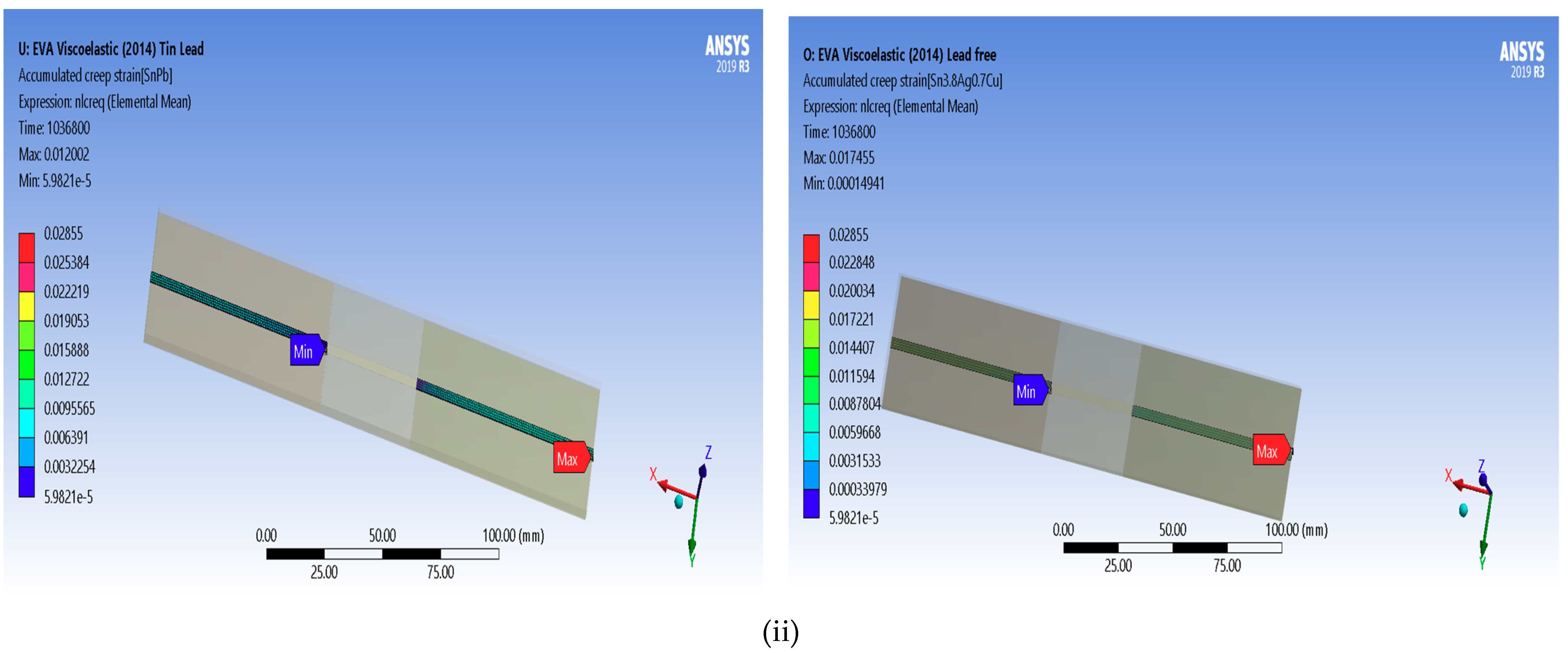
A maximum accumulated creep strain damage of 0.028555 mm/mm was generated in the Pb-free solder interconnection during the 2012 thermal load cycle (
Figure 10ii) and the minimum accumulated creep strain of 0.012002 mm/mm (
Figure 11ii) in the SnPb solder interconnection during the 2014 thermal load cycle. Overall, the 2012 thermal cycle induced the maximum accumulated creep strain in both interconnections (0.01988 mm/mm for SnPb solder and 0.028555 mm/mm for Pb-free).
Table 7 presents a summary of the percentage change in accumulated creep strain from the SnPb solder interconnection to the Pb-free solder interconnection. It was observed that for the 2012, 2013 and 2014 thermal cycles, the accumulated creep strain damage increases by an average value of 45% when the interconnection solder is changed from an SnPb solder to Pb-free solder. However, the increase in accumulated creep strain was lower than the 57.96% increase resulting from the TRA cycle. The value of 57.96% must be the true value for the test region since it uses the average of the temperature load data from 2012–2014, as previously indicated.
Displayed in
Figure 12 is the accumulated creep strain response over the 12 thermal cycles. The response of accumulated creep strain over the 12 thermal cycles presented in
Figure 12 shows that, for up to the third thermal cycle, the accumulated creep strain damage response in the Pb-free solder interconnection remained largely unchanged for the 2013, 2014 and TRA cycles.
After the third thermal cycle, however, variations in the cumulative creep strain response become more pronounced. The damage accumulation in the Pb-free solder for the 2013 and 2014 thermal cycles was slightly lower than during the TRA thermal period at the end of the 12 thermal cycles. The cumulative creep strain damage per cycle from the 2012 thermal cycle was found to be higher than that of the TRA thermal cycle, while using the same Pb-free solder interconnection. Similarly, for the 2013, 2014 and TRA periods, the cumulative creep damage response remained roughly equal up to the second thermal cycle with the SnPb solder interconnection. This trend continued with the 2013 and TRA cycles, which remain unchanged until the end of the 12 thermal cycles. However, the accumulated creep strain responses for the 2014 thermal cycle produced a relatively lower accumulated creep strain per cycle after the second thermal cycle and until the end of the 12 thermal cycles. This observation confirms what has been reported previously by Amalu and Ekere [
41], who observed that, for a given thermal loading cycle, more than three thermal cycles are required to effectively assess creep damage in solders. Fewer than four thermal cycles may generate misleading results. It was observed further that the 2012 thermal cycle generated a relatively higher creep strain damage per cycle in the SnPb solder interconnection. The results from the accumulated creep strain show that the fatigue life of Pb-free solder interconnections is expected to be relatively lower as compared with SnPb solder interconnects at the test site. However, Syed [
37] observed that the accumulated creep strain displays sensitivity to the type of constitutive equation used in modeling the behavior of the solder joint. Additionally, the accumulated creep strain is unable to capture damage resulting from low-temperature dwells effectively. On the other hand, the accumulated creep energy density (
) parameter can capture the damage from low-temperature dwells and does not display noticeable sensitivity to the constitutive model of the solder. Thus, the accumulated creep energy density offers a comparatively better parameter for fatigue life prediction in solder joints. In the next section, the accumulated creep energy density in the solder interconnections generated by the thermal cycles is evaluated.
3.4. Evaluation of Accumulated Creep Energy Density (ACED) in Solder Interconnections
In
Section 3.4, the cumulative creep energy density (ACED) was determined for the 2012, 2013, 2014 and TRA thermal cycles in Ansys using the creep work command NL CRWK.
Figure 13 summarizes and describes the ACED distributions at the end of 12 thermal cycles.
Figure 13 shows a column plot of cumulative creep energy density for the four thermal cycle profiles at the end of 12 thermal cycles. During the TRA thermal cycle, replacing the SnPb solder with a Pb-free solder interconnection resulted in a maximum percentage change of 71.4% (from 1.3573 × 10
5 J/mm
3 to 2.3275 × 10
5 J/mm
3) in accumulated creep energy density. The 2013 thermal cycle, on the other hand, saw a minimum change in cumulative creep strain energy density of 43.56%. As a result, the TRA thermal cycle has a higher sensitivity to solder interconnection material properties than the 2013 thermal cycle, which has a lower sensitivity to solder interconnection material properties.
Figure 14 shows the time-dependent cumulative creep energy density for the two separate solder interconnection materials over various thermal cycle profiles. The accumulated creep energy density profiles for 2013 and TRA thermal cycles remained roughly similar for up to six thermal cycles with the Pb-free solder interconnection, as shown in
Figure 14. The accumulated creep energy density profiles for 2013 and TRA for the SnPb solder interconnection remained the same for up to the third thermal period. Furthermore, the ACED profile produced in the Pb-free interconnection during the TRA cycle shows a higher ACED per cycle from the sixth to the end of the 12th thermal cycle than the 2013 cycle. In comparison, the ACED profile for the TRA thermal cycle produced in the SnPb solder interconnection shows a lower ACED than the 2013 thermal cycle after the third thermal cycle. The findings show that more than six thermal cycles are needed to accurately measure ACED damage in the solder interconnection.
4. Conclusions
The creep damage of the solder interconnection in a solar PV is evaluated in this study for both SnPb and Pb-free solders. For the years 2012, 2013 and 2014, the study used thermal cycle loads produced by real-time monitoring of module temperatures on installed PV modules. This research also made use of a test area average (TRA) thermal cycle established in a previous study. The 2012 thermal cycle caused maximum stress and creep strain damage of 9.0148 MPa and 0.010393 m/m, according to the results of the numerical analysis. The maximum stress and creep strain in the SnPb solder interconnection were measured. During the 2013 thermal cycle, the minimum equivalent stress and creep strain damage in the Pb-free solder interconnection were 7.9169 MPa and 0.0055175 m/m, respectively. The Pb-free solder interconnection accrued the most creep strain damage during the 2012, 2013 and 2014 thermal cycles, according to the accumulated creep strain results. The average percentage change in cumulative creep damage obtained by replacing the SnPb solder interconnection with a Pb-free solder was found to be approximately 45% over these three thermal cycles. Under the TRA thermal cycle, the change in cumulative creep strain was found to be higher when the SnPb solder interconnection was substituted with a Pb-free solder (57.96%). During the TRA thermal cycle, the SnPb solder was replaced with a Pb-free solder interconnection, resulting in a maximum percentage change of 71.4% in accumulated creep energy density. At the KNUST test site in Kumasi, Ghana, this study found that Sn60Pb40 solder interconnections are likely to be more reliable than Sn3.8Ag0.7Cu (Pb-free) solder interconnections. To predict damage in soldered interconnections, the analysis can be replicated at different test sites.


