Article

Strategies for High-Performance Large-Area Perovskite Solar Cells toward Commercialization

1
Department of Physics, Shaoxing University, Shaoxing 312000, China
2
Zhangjiang Lab, Shanghai Synchrotron Radiation Facility (SSRF), Shanghai Advanced Research Institute, Chinese Academy of Sciences, 239 Zhangheng Road, Shanghai 201204, China
3
Shanghai Institute of Applied Physics, Chinese Academy of Sciences, 2019 Jialuo Road, Shanghai 201800, China
4
Egyptian Petroleum Research Institute, Nasr, Cairo 11727, Egypt
5
Helmholtz-Zentrum Berlin für Materialien und Energie GmbH, Hahn-Meitner-Platz 1, Berlin 1410, Germany
6
Sch Microelect, State Key Lab ASIC & Syst, Shanghai Inst Intelligent EI Elect & Syst, Fudan University, Shanghai 200433, China
*
Authors to whom correspondence should be addressed.
These authors contribute equally to this paper.
Crystals 2021, 11(3), 295; https://doi.org/10.3390/cryst11030295
Submission received: 9 February 2021 / Revised: 24 February 2021 / Accepted: 25 February 2021 / Published: 16 March 2021
(This article belongs to the Section Inorganic Crystalline Materials)

Abstract

:
Perovskite solar cells (PSCs) have received a great deal of attention in the science and technology field due to their outstanding power conversion efficiency (PCE), which increased rapidly from 3.9% to 25.5% in less than a decade, comparable to single crystal silicon solar cells. In the past ten years, much progress has been made, e.g. impressive ideas and advanced technologies have been proposed to enlarge PSC efficiency and stability. However, this outstanding progress has always been referred to as small-area (<0.1 cm2) PSCs. Little attention has been paid to the preparation processes and their micro-mechanisms for large-area (>1 cm2) PSCs. Meanwhile, scaling up is an inevitable way for large-scale application of PSCs. Therefore, we firstly summarize the current achievements for high efficiency and stability large-area perovskite solar cells, including precursor composition, deposition, growth control, interface engineering, packaging technology, etc. Then we include a brief discussion and outlook for the future development of large-area PSCs in commercialization.

1. Introduction

Since the industrial age, the energy used by people has generally been fossil energy. The energy used by people earlier was mainly wood, in the 19th century, coal began to be used on a large scale, and oil and natural gas were used in the 20th century. The use of these fossil energy sources will inevitably cause environmental pollution and seriously affect people’s health. For example, in the 19th century, London turned into a smog city, and China’s smog, in previous years produced huge amounts of greenhouse gases (such as CO2, CH4), causing global warming and climate deterioration. Fossil energy is a non-renewable energy source. Therefore, people have begun turning their attention toward renewable energy, among which, solar energy is undoubtedly the best, and use of solar cells is currently the most crucial way to make use of solar energy, by converting it into electric currents that could be utilized.
In recent years, perovskite solar cells (PSCs) have attracted worldwide attention due to their unique advantages. In just ten years, the PCE of PSCs has jumped from 3.8% [1] to 25.5% [2] presently; it can be seen that it has great development potential and application prospects. However, most of the current PSCs are organometallic halide PSCs, which are easily affected by temperature and humidity, resulting in poor stability, and many of them are small-area PSCs, so they are not successfully embarked on the road of commercial production. Recently, Seo et al. in South Korea have developed a PSC with an area of 100 cm2 and a PCE of 18.8% [3]; and Groen et al. in the Netherlands have developed PSCs with an area of 144 and 160 cm2 with a PCE of 14.5% and 11% [4]. Meanwhile, Boyd et al. explained the degradation mechanism of perovskite-type optoelectronic materials and greatly improved their stability [5]. Miyasaka et al. provided in detail, the background, current situation, and prospects of halide perovskite photoelectric materials [6]. In this review, show the possibilities of PSC commercialization.

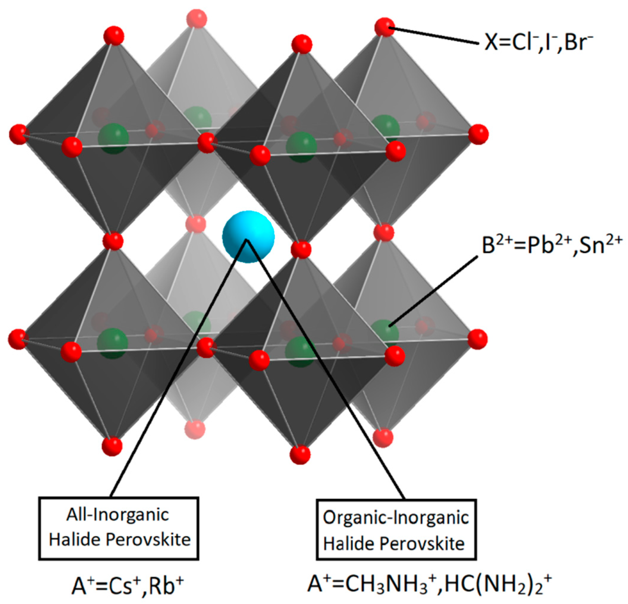
2. Crystal Structure of Perovskite Materials

The word perovskite was given to commemorate the discovery of CaTO3 by Russian mineralogist Lev Provski’s team in 1983 [7]. Now, the perovskite in PSCs refer to metal halide perovskite; its general chemical formula is ABX3. A position is usually a monovalent metal cation, such as Cs+ or Rb+, and it can also be an organic cation, such as methylamine and formamidine, etc. TheB position could be divalent metal cations Pb2+, Sn2+, Bi2+, etc.; X position is usually I, Br,Cl and other halogen anions [8]. The stability of the crystal structure is usually determined by the tolerance factor t, which is expressed as:
t = R A + R B 2   ( R A + R X )
R A , R B , R X represent the ionic radius of the corresponding ions. When t lies in the range 0.8–1.0, the cubic structure of Figure 1 is likely to occur. When t is very small, the form of perovskite crystal will become a tetragonal or orthorhombic structure it will also become a cubic structure when it is subjected to a high temperature treatment. [9] In addition to t, there is another critical parameter that will affect the stability of the crystal, which is the octahedral factor μ , expressed as [10,11]:
μ = R B R X
R B , R X represents the ion radius of the corresponding ion. When μ is between 0.4 and 0.9, it helps to form a stable BX6 octahedron. The BX6 octahedron also undergoes lattice distortion with changes in temperature, pressure, and stoichiometric ratio, leading to a series of phase transition processes [12].

3. Research Progress of PSCs

Figure 2 shows the efficiency transition of PSCs from 2009 to 2020. In 2009, Miyasaka et al. designed the first PSC, which used CH3NH3PbI3 deposited TiO2 electrode as the photoelectrode (anode) and platinum-coated F-doped SnO2 glass as the counter electrode (cathode). The cathode and anode were inserted into a 50 μm thick separation membrane, and the middle was filled with an organic electrolyte solution containing lithium halide and halogen. The effective light exposure area was 0.238 cm2, and the highest PCE achieved was 3.8% [1].
In 2011, Park et al. deposited a layer of 3.6 mm perovskite quantum dots on TiO2 and prepared a quantum dot-sensitized solar cell based on perovskite CH3NH3PbI3 as a sensitizer. The conversion efficiency reached 6.8%, but it was degraded to 80% within 10 min. The stability was very poor, and continuous research was needed to improve it [13].
In 2012, Snaith et al. reported a mixed-halide form (CH3NH3PbI2Cl) perovskite that exhibitedpower conversion efficiency near 11% [12]. They used the solid hole transport layer spiroOMeTAD(2,2(7,7(-tetrakis-(N,N-di-pmethoxyphenylamine)9,9(-spirobifluorene))) as the transparent P-type hole conductor, and replaced mesoporous TiO2 with Al2O3 as the transparent N-type component. The Al2O3 has a wide band gap (7–9 eV), allowing Al2O3 to act as perovskite “scaffold” with mineral coating. This is conducive to the improvement of the electron transmission speed and open circuit voltage. Ultimately, the PCE of PSCs increased to 10.8% [14]. In 2013, Snaith et al. prepared a mixed halide perovskite CH3NH3PbI3-xClx film using a vapor deposition method with dual sources. The PCE of PSCs reached 15.4% [15]. Later, people began to design new mixed -halide perovskite films to improve the PCE.
In 2014, Zhou et al. increased the PCE to 19.6% by suppressing the recombination of carriers [16]. In 2015, Yang et al. used the formamide lead iodide (FAPbI3) perovskite, which had a bandgap that could absorb the solar spectrum more widely. It was prepared by an intramolecular exchange between dimethyl sulfoxide (DMSO) and methylammonium iodide. Then, its PCE reached 20.2% [17]. This PCE is basically consistent with the PCE of silicon-based solar cells, so more people have begun to focus on preparing PSCs with a larger area and better stability. In the same year, Hen et al. designed large-area PSCs with an area of 1.017 cm2 and a PCE of 15%. This PCE has passed the certification of an independent certification body. The manufacturing method of the large-area PSCs is based on using a heavily doped inorganic charge extraction layer in the planar PSCs. Even if the extraction layer is 10–20 nm, the carrier can be extracted very quickly, which can avoid pinholes and eliminate local structural defects caused by large areas. Another stability milestone was achieved. Under 1000 h of light irradiation, the PCE can still be greater than the initial 90% [18]. In 2019, his team produced soft PSCs with an aperture area of 1.02 cm2 and a PCE of 22.1%. The method is to use a solution treatment strategy, utilizing a diluted Pb(SCN)2 solution as a Pb source, spin coating on the surface of the perovskite film, and then removing FASCN (methylamine thiocyanate) or MASCN (methyl thiocyanate) and other volatile organic components, forming a Pb-rich perovskite film on the surface, which will form strong chemical bonds on the surface of the soft perovskite film to stabilize the heterostructure of the perovskite, which will largely reduce the loss of the perovskite film, so that it can maintain 90% of its initial PCE after 1000 h of operation under the sunlight of 60 °C and AM1.5 [19].
In 2016, Grätzel et al. used polymethyl methacrylate (PMMA) as a template to prepare a high-quality perovskite film, which can effectively control nucleation and crystal growth, and due to the reduction of the nucleation free energy, heterogeneous nucleation speed is several orders of magnitude faster than uniform nucleation. Finally, a PSC with a PCE of 21.6% was achieved, and the certification PCE reached 21.02% [20].
In 2017, Yang et al. introduced additional iodide ions into the organic cation solution to form a perovskite layer through an intramolecular exchange process, reducing the concentration of defects in the deep energy level, making the PCE of the small-area PSCs prepared to reach 22.1%, and the PCE of the large-area PSCs with an area of 1 square centimeter was 19.7% [21].
In 2018, Lee et al. synthesized a terminal fluorene hole transport material with fine-tuned energy level and high glass transition temperature to ensure the high efficiency and stability of PSCs. The certified PCE of the small-area (0.098 cm2) PSCs reached 22.6%, and the certification PCE of the large-area (1 cm2) PSCs reached 20.9%, and it can work for more than 500 h in an environment of 60 °C and still maintain 95% of the initial PCE [22].
In 2019, Kim et al. systematically studied the effect of methylammonium chloride (MACl) additives in FAPbI3-based perovskites. Using the density functional theory, it could be concluded that the incorporation of MACl will affect the formation of the perovskite structure. When 40 mol% MACl is added, the best PSC can be manufactured, the grain size increased by six times, the phase crystallinity increased by three times, and the photoluminescence lifetime increased by 4.3 times. The highest PCE reached 24.02%, and the certification PCE reached 23.48% [23].

4. Challenges and Solutions for Manufacturing Large-Area PSCs

Before 2015, most studies focused on the properties and stability of PSCs, the area of PSCs, is generally less than 0.1 cm2. Many studies were pursuing high PCE to prove that PSCs were not weaker than other solar cells. In 2015, the PCE of PSCs broke through 20%, which is at the same level as the PCE of silicon-based solar cells. After that, scientists began to focus on designing large-area PSCs with bigger size and greater stability, and, finally, can be commercialized. This year, Han et al. published their work in Science [18], in which the concept of large-area PSCs was proposed. In this work, they designed PSCs with an area larger than 1 cm2, and the PCE reached 15%. Moreover, its stability had also been greatly improved; after 1000 h of work under light irradiation, it retains more than 90% of the initial PCE. Subsequently, more people began to prepare large-area perovskite films. The area of PSCs is mainly about 1 cm2 because as the area increases, the stability and PCE of the PSCs will decline rapidly. It is challenging to have the best of both worlds.
After 2015, more people began to manufacture large-area perovskite films, but there was always a significant gap in PCE between large-area and small-area PSCs. As the area of PSCs increases, the stability and PCE of PSCs will decline rapidly, as shown in Figure 3. There are three main reasons for these behaviors. Firstly, when the device active area becomes larger, the crystal uniformity in perovskite film will inevitably decrease, and cells in series will lead to an increase in resistance. Secondly, the repeatability of large-area PSCs is poor. When manufacturing small-area PSCs in a laboratory, it is generally under a strict environment (control of humidity and temperature). In order to achieve excellent PCE, the cost is not considered. However, there are no such conditions for large-area PSCs, we have to manufacture PSCs that can be used generally in reality, and tolerant to the environment. Thirdly, people have just transitioned from small-area to large-area PSCs; the method of manufacturing small-area PSCs is not suitable for manufacturing large-area PSCs. For example, a spin-coating process is generally used to manufacture small-area PSCs instead of blade coating or slot-die coating. However, to manufacture large-area PSCs, blade coating and slot-die coating are needed.
Currently, there are mainly six ways to increase the efficiency and stability of large-area PSCs.
(1) Find a suitable process for manufacturing large-area PSCs and improve this process. In the past, the spin-coating process was generally used to manufacture small-area PSCs, but this is not suitable for large-area PSCs. Currently. more processes that could be used to manufacture large-area PSCs. For example, blade coating [24,25], slot-die coating [26,27,28], inkjet printing [29,30,31], screen printing [32,33], spray coating [34,35], vapor phase deposition [35,36,37] and electrodeposition [38,39]. These processes can more effectively manufacture large-area solar cells.
(2) The efficiency and stability of the PSCs can be improved by improving the precursor solution or finding materials with better performance (including longer carrier diffusion length, higher absorption coefficient, etc.). These factors will effectively help us make PSCs with better efficiency and larger areas.
(3) Add better additives to the precursor solution. Adding different additives will have different effects. For example, adding thiourea or thiosemicarbazide to MAPbI3 precursor can increase the grain size of perovskite film and improve device performance [40,41]. Adding cadmium (Cd) and aluminum (Al) ions can increase photoluminescence and reduce electron defect density [42,43]. Adding lead thiocyanate (Pb(SCN)2) and PCBM ([6,6]-phenyl-C61-butyric acid methyl ester) can improve the fill factor of device performance [44,45].
(4) Interface engineering. Good interface matching can reduce or even eliminate the J-V (current-voltage) hysteresis of PSCs, thereby reducing the interface recombination and improving PSC stability and PCE.
(5) Packaging technology, encapsulation of PSCs is essential, which can help PSCs avoid interference from the external environment, limit the exposure of oxygen and moisture, and greatly improve PSC stability.
(6) Growth control. By artificially controlling the growth of perovskite crystals, perovskite films with larger grains and better uniformity can be grown, improving the PCE and stability of PSCs.
The following is a specific introduction to the achievements of these six methods.

4.1. Processes Improvement

In 2016, Grätzel et al. used the most advanced perovskite FA0.81MA0.15PbI2.51Br0.45 and a simple way to design large-area perovskite films. The method was a vacuum flash solution treatment, which can quickly control solvent’ removal and promote fiber material rapid crystallization. After thermal annealing, highly oriented perovskite crystal films with excellent electronic quality can be grown on various substrates, and the hysteresis in the current-voltage (J-V) curve is eliminated. A large-area cell with an area of 1 cm2 was obtained. The maximum PCE was 20.5%, and the certified PCE reached 19.6% [46].
In 2018, Groen et al. considered that it was necessary to improve a process to deposit the constituent layers over large areas efficiently, so they optimized the application of the slot die coating process in sheet-to-sheet (S2S) and roll-to-roll (R2R) manufacturing. Moreover, the uniformity of perovskite crystallization is controlled by adjusting the ink formulation and drying process. This technique helps large-area perovskite film without excessive loss even after an increase of thee orders of magnitude (from 0.09 cm2 to 144 cm2). Finally, a large-area PSC of 144 cm2 was manufactured (Figure 4), with a stable PCE of 13.8% and an active-area PCE of 14.5% [4].
In the same year, Seo et al. proposed a fast and simple two-step method to design high-quality perovskite films, namely mediator extraction treatment (MET) [3]. Compared with other methods for fabricating perovskite films, this method can significantly improve the preparation of large-area PSCs. The two most representative methods are solvent engineering and two-step sequential deposition. The crystal growth process of solvent engineering usually only takes a few seconds, and the repeatability is poor, especially for large-area perovskite films; The two-step sequential deposition is a more controllable and reliable method that can fabricate large-area perovskite films with high uniformity. However, it takes at least one hour when the PbI2 layer is completely transformed into perovskite, which is too long. MET can significantly reduce the time of this step. They first deposited PbI2-DMSO film, then DMSO mediators were extracted efficiently and rapidly by optimizing casting solvent and anti-solvent. Afterward, the PbI2 film can form a porous morphology with relatively random crystal orientation within a few seconds, helping PbI2 to be wholly and quickly converted into perovskite. In this way, a 100 cm2 PSC was fabricated (Figure 5). The maximum PCE of PSCs fabricated using spin coating is 18.8%, and the maximum PCE of PSCs fabricated using slot-die coating is 18.3%.
In 2020, Mai et al. used the self-assembly one-step printing process to manufacture 2D/3D heterostructure MAPbI3 for the first time. Unlike the previous two-step deposition to prepare 2D/3D heterostructures, they grew a thin layer of two-dimensional perovskite in situ on top of the 3D-MAPbI3 perovskite body. Because of the amine (-NH2) and carboxyl (-COOH) functional groups in the macromolecular SBLC, it can repair the charged defects of the perovskite and reduce non-radiative recombination [47,48,49]. Secondly, better 2D/3D interfaces can be obtained through the interaction of the hydrogen-halogen bonding and the 3D Perovskite, thereby reducing the 2D/3D interface recombination. Thirdly, due to unpaired electrons in the sulfur atom, SBLC can act as a Lewis base and cooperate with PbI2 to increase crystal size by slowing down crystal growth [50]. Through one-step scraping and vacuum quenching crystallization, a thin layer of 2D perovskite can be perfectly self-assembled to cover the surface of 3D Pperovskite. The 2D layer of Perovskite on the surface can effectively passivate the surface defects of the 3D Perovskite, inhibit non-radiative recombination, and greatly increase the open circuit voltage. Finally, large-area PSCs with an active area of 10.08 cm2 was manufactured, and its PCE was as high as 15.38%. It also has good thermal stability and light stability and can retain 80.9% of the original PCE after 30 days of storage in ambient air [51].

4.2. Improvement of the Precursor Solution and Better Materials Utilization

In 2017, Marks et al. used a one-step hot-casting perovskite system, which is different from the original use of PbI2 and MACl to make MAPbI3. They used PbI2 and MAI salts (1:1 molar ratio) to hot-cast MAPbI3. This method can control the incorporation of Cl- to reduce recombination, increase the carrier diffusion length, and improve the perovskite film’s morphology and the halide concentration gradient in the entire perovskite film. In addition, Cl- can also enhance the stability of the device by passivating the reaction between I- and the silver electrode. Using this method, a 25 cm2 perovskite film was fabricated by the dip-coating process, and the active-area PCE is 12% [52].
In the same year, Huang et al. created a new type of quadruple-cation perovskite absorber KxCs0.05(FA0.85MA0.15)0.95Pb(I0.85Br0.15)3 (denoted as KCsFAMA) by adding potassium ions. Its most outstanding feature is that it can eliminate the hysteresis in PSCs. It also has good stability and can keep the efficiency unchanged even after 1000 h of storage in the ambient air. The addition of potassium can also help the perovskite film crystallize quickly, and the resulting grain size is as high as 1 µm, which is twice the size of the control film without potassium. With KCsFAMA, perovskite films with lower interface defect density, longer carrier lifetime, and faster charge transfer speed can be produced. In this work, 6 × 6 cm2 PSCs were fabricated with an active area of 20 cm2 and a PCE of 15.76% [53].
In 2019, Bonaccorso et al. pioneered the use of 2D graphene and functionalized MoS2 in PSCs. The use of 2D materials effectively improved the stability and overall PCE of the PSCs and successfully fabricated a large-area PSC of 108 cm2. The PCE of the active area reached 13.4%, and it can work at 65 °C for 1000 h; its PCE can retain 75% of the initial value [54].
In 2020, Jeong et al. wanted to optimize the organic hole transport materials (HTM). However the latest HTM, including cesium cation [55,56], carbon electrode [57,58,59], and dopant free-based PSCs [60,61], has lower PCE than Spiro-OMeTAD-based PSCs. They decided to optimize Spiro-OMeTA by taking into account multiple possible aspects of the fluorination of conjugated materials (for example, dipoles induced by C-F bonds reduce energy levels and enhance molecular packing and hydrophobicity), two fluorinated isomeric analogs (Spiro-mF and Spiro-oF) were developed as HTMS for PSC preparation (Figure 6 shows Chemical structures of Spiro-OMeTAD and its fluorinated analogs Spiro-mF and Spiro-oF). Compared to the optimized Spiro-OMeTAD-based PSC, it is found that the performance of the PSC made with Spiro-mF is superior. Its PCE is 24.82% (certified PCE is 24.64%, the loss is 0.3 V), and it can still maintain 87% of the original PCE after 500 h under high relative humidity and no packaging. Besides, the fabricated 1 cm2 large-area PSC has a PCE of 22.31% [62].

4.3. Additives Addition to the Precursor Solution

In 2019, by improving the additives added to the precursor solution, Deng et al. created an unprecedented method that can quickly coat a large area of perovskite film at a speed of 99 mm/s at room temperature. In order to have this speed, they studied dimethyl sulfoxide (DMSO), dimethylformamide (DMF), gamma-butyrolactone (GBL), 2-methoxy ethanol (2-ME), and acetonitrile (ACN) coordination ability with MAPbI3 [63,64]. They found that common solvents (such as DMSO and DMF) are not conducive to the rapid deposition of dense and smooth perovskite films at room temperature. The high volatility of 2-ME and ACN will result in low crystallinity of perovskite films and poor contact to the substrate. However, when the two solvents are combined in a particular ratio, it is surprisingly found that this new additive not only has the advantages of both but also avoids their disadvantages. In addition, new additives were slowly released from the coated solid film, thereby providing enough time for the perovskite grains to grow into a large-size perovskite film with high crystallinity and good contact with the substrate. Finally, a PSC with excellent resistance to temperature and shading was manufactured, with an aperture area of 63.7 cm2 and a certification PCE of 16.4% [65].
In 2019, Huang et al. discovered a new class of additives; that is, surfactants (for example, L-α-phosphatidylcholine). As long as a very small amount of surfactant is added, the solution flow dynamics in the dry ink layer can be significantly inhibited, and the adhesion of the perovskite ink to the underlying non-wetting charge transport layer can be increased. This facilitates the solution deposition of large-area pinhole-free organic-inorganic perovskite films. Some surfactants also have a passivation effect, which can further improve device performance. In their research, they added 20 ppm of surfactant to the perovskite ink, which helped them to obtain high-quality perovskite films at a high-speed coating of 180 mm/h. The PCE of the small-area PSCs obtained by this method is more than 20%. When the aperture area is 33.0 cm2 and 57.2 cm2, the PCE of 15.3% and 14.6% are obtained, respectively [66].
In 2020, Huang et al. used a slot-die coating process and then heated it with near-infrared radiation. They then added a low boiling point and low surface tension n-butanol to the precursor solution to increase near-infrared energy absorption. Promote the evaporation and film formation of the solvent system and accelerate the crystallization of perovskite. Finally, four layers of 12 × 12 cm2 uniform and high-quality perovskite film can be fabricated within 18 s, and its PCE reached 10.96%. (Figure 7 and Table 1) The fabricated single-layer 12 × 12 cm2 large-area PSC with a PCE of 14.3% [67].

4.4. Interface Engineering

In 2016, Wang et al. realized that interface engineering and perovskite crystallization are the most critical factors for realizing high-performance planar heterojunction PSCs. Therefore they demonstrated a solution processing method to make thin perylene as the underlayer of PSCs. (Figure 8) Using branch-shaped perylene film as a seed-mediated underlayer can form perovskite crystals with a textured morphology, thereby significantly improving absorption through light scattering effects. Because the perylene has a deep highest occupied molecular orbital (HOMO) energy level, it also plays a vital role in poly(3,4-ethylene dioxythiophene): poly(styrene sulfonate) (PEDOT:PSS), and CH3NH3PbIxCl3−x energy level tailoring. In addition, perylene and perovskite form a complete crystalline heterostructure, which helps to minimize defect and trap densities. Due to these advantages, the PCE of PEDOT:PSS based PSCs is increased from 12% to more than 17%, which reduces the J-V hysteresis effect and improves the stability of the device. This technique provides a simple way to control the crystallization of perovskite and optimize the interface in the planar heterostructure PSC [76].
In 2017, Tan et al. believed that performance and stability losses of low-temperature planar PSCs may be caused by the imperfect interface and charge recombination between the selective contact on the illumination side and the perovskite film grown on top [77,78,79], because the perovskite active layer itself has good long-term light stability after adding formamidinium (FA), Cs and Br ions [18,47,56,80,81]. They believe that when the perovskite film has an excellent long photocarrier diffusion length, attention should be directed to the perfect interface [82,83,84,85]. Therefore, they used a modified TiO2 nanocrystalline film formed by doping Cl ions as an electron selective layer, which can reduce interfacial recombination and improve the interfacial bonding of low-temperature planar PSCs. After the produced solar cell is treated with a low-temperature solution, the final area is 1.1 cm2, and the PCE is as high as 20.1%. Moreover, it also pronounced high stability, after 500 h of continuous operation at room temperature with the maximum power under one sun illumination, its performance remains 90% of the initial value (97% after dark recovery) [86].
In 2019, Yang et al. wanted to develop a high-quality electron transport layer (ETL) with suitable energy levels and high electron mobility. However, the charge carrier transport efficiency is also very sensitive to the morphology of various interfaces in the PSCs; the interface morphology between ETL and perovskite must be controlled to promote carrier transport to obtain ideal device performance [87]. They used a new low-temperature processing SnO2 instead of TiO2, which has a more suitable energy level and higher electron mobility [88,89]. However, the mobility of SnO2-ETL (10−3 cm2V−1s−1) is very low compared to CH3NH3PbI3 (0.5−30 cm2V−1s−1) [90,91], this is not suitable as an ETL candidate. Therefore, they used red-carbon quantum dots (RCQs) rich in carboxylic acids and hydroxyl groups doped with low-temperature solution-treated SnO2 to produce effective composite ETL. This significantly increased its electron mobility from 9.32 × 10⁻⁴ to 1.73 × 10⁻² cm2V−1s−1, which is about a 20 time increase (this is the highest electron mobility of SnO2) (Figure 9). After RCQs doping, the surface of SnO2 becomes more hydrophilic, which indicates that the Gibbs free energy on the surface is reduced, which is conducive to the non-uniform nucleation of perovskite and produces high-quality perovskite films [92]. The PCE of the new SnO2-ETL planar PSCs was increased from 19.15% to 22.77%. Moreover, the long-term stability against humidity was enhanced. After 1000 h at 25 °C and 40–60% humidity, it still maintains a PCE of 95% of the initial efficiency [93].

4.5. Packaging Technologies

In 2016, Bella et al. prospected to improve the stability and efficiency of PSCs through packaging technology. Some groups reported the hydrophobic polymer layers to limit atmospheric moisture [94,95], others used metal oxide (for example, chromium oxide-chromium (Cr2O3/Cr)) interlayers to protect organic components, protect metal contacts from the reaction of perovskite materials, and produce PSCs with all-solution-processed metal oxide charge transport layers [96,97,98]. These methods are only considering the damage of the air to the device. Bella et al. used a multifunctional photopolymer as an excellent solution to solve PSCs instability. Moreover, a luminescence downshifting (LDS) fluoropolymer layer is rapidly photogenerated on the front side of the device (i.e., the glass surface). The coating prevents the ultraviolet part of the incident solar spectrum from negatively interacting with the PSC stack by converting the ultraviolet part of the incident solar spectrum into visible light and increases the photocurrent by 6%. Due to atmospheric humidity tolerance, a robust hydrophobic photopolymer is grown on the back contact side. This additional layer acts as an effective barrier to prevent water penetration in the solar cell stack. The PCE of the finally manufactured PSCs was 18.67%. In the 180-day (4320 h) aging test, under different atmospheric conditions and various photochemical external stresses, the resulting device showed unparalleled stability. The same device was also exposed to a real outdoor environment for more than three months (2160 h), successfully demonstrating its excellent resistance to dust, soil, and heavy rain on the external glass surface. Finally, the low surface energy fluorinated LDS layer makes the front electrode easy to clean under actual outdoor conditions. In order to prove the water-resistance of the photopolymerized fluorinated coating, the PSC was put into a beaker filled with boiling water (95%RH). One month later, the PSC had 96% of the initial PCE [99].
In 2017, Lee et al. expected to improve the stability of PSCs through customized thin-film encapsulation (TFE) and then developed a new method to integrate TFE directly on the PSCs to improve the humidity resistance of the device. This method is an organic/inorganic multilayer TFE system, which is made by combining initiated chemical deposition (iCVD) and atomic layer deposition (ALD) processes [100,101,102]. A pair of Al2O3 inorganic layer and pV3D3 organic layer is called a dyad, which has excellent barrier properties. This is the first use of iCVD and ALD processes to apply multilayer TFE to PSCs packaging (Figure 10). In order to improve its long-term stability in a humid environment, the TFE structure and deposition conditions were optimized, and the purge time after water injection was adjusted to reduce the ALD process temperature to minimize equipment damage during the TFE deposition step. The first organic layer manufactured by iCVD serves as the main protective film for PSC. TFE was prepared at low temperature using 60 °C-ALD and 40 °C-iCVD processes to deposit pV3D3/Al2O3 multilayer films. Under the accelerated conditions of 38 °C and 90%RH, its water vapor transmission coefficient was 10−4 g m−2d−1, showed excellent barrier properties. Moreover, the packaging process is significantly improving the stability without degrading the performance of the device. The PSCs can be exposed to 50 °C and 50% relative humidity for 300 h, and its PCE still has 97% of the initial value [103].
In 2020, Emami et al. developed an advanced laser-assisted glass-frit encapsulation method to seal PSCs without hole transport material (HTM). They had already known that the performance loss of HTM-based PSCs is caused by the thermal instability of the HTM layer at 100 °C, moreover, the glass-frit has excellent airtightness and stability compared with ordinary thermoplastics, and the laser beam can locally heat the sealant material to its melting point while keeping the device at a lower process temperature. Since the laser-assisted sealing process temperature and dwell time will affect the performance of the PSCs device, they established a response surface method (RSM), model. The model included two-factor variables (sealing process temperature and heating dwell time) and three-factor responses (sealing quality, sealing reproducibility, and the effect of the sealing process on the performance of PSCs device) to minimize the above effects. They finally produced PSCs that can pass 70 thermal cycles (−40 °C to 85 °C) and 50 h of damp heat (85 °C, 85% RH) test according to the IEC61646 standard. This is the first report of the packaging method that can pass the airtightness requirements of the relevant PV standard test. In a humid air environment (80 ± 5% RH), the PCE of packaged PSCs remains unchanged, while non-hermetic packaged devices will degrade after about 50 h. It is worth mentioning that all packaged PSCs in this study still maintained stable performance after more than 15 months [104].

4.6. The Control of Perovskite Crystal Growth

In 2020, Lv et al. added a series of urea molecules (urea, biurea, or triurea) composed of Lewis base (–NH2) and Lewis acid (–C=O) groups to the perovskite precursor. Urea and biuret are conducive to the growth of large-grain crystals, and there is a correlation between –C=O and –NH2 groups and PbI2 and MAI. Triurea molecules are easy to aggregate and adhere to the surface of the perovskite to form a cascade junction, thereby reducing the barrier of electron transfer from the perovskite to the electron transport layer, and can improve the PCE of the device. In addition, depending on the different coordination abilities of the perovskite components, the bound molecules can change the crystallization kinetics. This allows large crystals to grow at low temperatures (60 °C) and associate with counter ions or insufficiently coordinate ions to passivate defects and enhance charge transfer. In order to obtain synergistic benefits from additive engineering, they tried to mix different combinations of additives such as urea/triurea, biuret/triuret, or urea/biuret into the precursor to improve device performance further. It was found that the biuret/triurea mixed additive is most conducive to the growth of large-particle crystals, and the best performance PSCs can be obtained, with a PCE of 21.6% [105].
In the same year, Huang et al. doped perovskite with diethyl ammonium bromide (DABr) and used in situ dynamic microscopy to study the grain growth mechanism of DABr-doped MAPbI3. The MAPbI3 was doped with different proportions of DABr. The results showed that the addition of 10% DABr could obtain a thin film with larger grains (about one μm) and uniform morphology, which can ensure that the electrode can effectively transport and extract carriers. Moreover, the film has fewer interface traps and can inhibit recombination. This could be due to the alkyl chain of DABr that inhibits the grain growth of MAPbI3 during the spin coating process and induces the crystal grains to merge during the annealing process to obtain micron-sized large grains. It should be concluded that DABr significantly improves the crystallization of MAPbI3 and reduces the number of defects. The PCE of the obtained PSCs is 19.58%, and the fill factor is 79.81% [106].

5. Discussion and Outlook

With the continuous development of science and technology, humanity’s demand for energy is increasing, so the development of sustainable energy is vital. Solar cells can meet this requirement. With the emergence of PSCs, a large number of scientific and technological personnel have devoted themselves to this. Because it has developed rapidly in just ten years, the PCE has increased from 3.8% to 25.2%. Moreover, it has excellent light absorption performance, a suitable energy band structure, and a bandgap of 1.5 eV, which is more ideal than silicon-based solar cells. Therefore, the development prospects of PSCs are undoubted, but there is still a long way to go before its commercialization because the fabrication of large-area and stable PSCs has always been problematic. In particular, as the active area of single solar cell becomes larger, its PCE will become lower. The organic components contained inside are volatile and, therefore, very unstable. However, people continue to explore it, through continuous improvement of precursor engineering and formulation, using more advanced interface engineering to effectively passivate defects, reduce non-radiative recombination, and reduce interface and grain boundary recombination, which have speeded up the preparation of high-quality perovskite films.
Meanwhile, the production and monitor of high-quality perovskite films are inseparable from the advanced characterization techniques, such as SIMS, GIWAXS, and cryo-electron microscope, etc., which help to reveal the in-situ forming film process, crystalline, and their micro-mechanisms for large-area perovskite solar cells. Therefore, the further development of in-situ dynamic characterization techniques and their joint utilization must be other focus points in the future. This would significantly promote the production of large area preparation strategies for PSCs, in order to accelerate the commercial process of PSCs. Predictably, we will eventually produce non-lagging, ultra-stable, and high-efficiency PSCs so that it could be commercialized and provide a force for future energy demand.

Author Contributions

T.D., Q.C., L.Y. and M.H.A.: writing original draft. L.Y., Y.D., and Y.Y.: writing-review & editing. H.L., M.L. and Q.L. are contributing the discussions. All authors have read and agreed to the published version of the manuscript.

Funding

This work is supported by the National Natural Science Foundation of China (Grant nos.U1632121, 11304204), Shanghai Municipal Commission for Science and Technology (No. 20ZR1464100), and the Youth Innovation Promotion Association CAS. We thank the Natural Science Foundation of Zhejiang Province (Grant Nos. LQ13A050002, LQ13A040003).

Acknowledgments

We thank the staff from BL01B1, BL11B, BL14B1, BL17B1, BL17U1 and BL19U1 beamlines of Shanghai Synchrotron Radiation Facility for assistance.

Conflicts of Interest

The authors declare that they have no known competing financial interests or personal relationships that could have appeared to influence the work reported in this article.

References

  1. Akihiro, K.; Kenjiro, T.; Yasuo, S.; Miyasaka, T. Organometal halide perovskites as visible-light sensitizers for photovoltaic cells. J. Am. Chem. Soc. 2009, 131, 6050–6051. [Google Scholar]
  2. NREL, Best Research-Cell Efficiencies. Available online: https://www.nrel.gov/pv/cell-efficiency.html (accessed on 30 September 2020).
  3. Kim, Y.Y.; Park, E.Y.; Yang, T.Y.; Noh, J.H.; Shin, T.J.; Jeon, N.J.; Seo, J. Fast two-step deposition of Perovskite via mediator extraction treatment for large-area, high-performance perovskite solar cells. J. Mater. Chem. A 2018, 6, 12447–12454. [Google Scholar] [CrossRef]
  4. Giacomo, F.D.; Fledderus, H.; Gorter, H.; Kirchner, G.; De Vries, I.; Dogan, I.; Verhees, W.; Zardetto, V.; Najafi, M.; Zhang, D. Large area > 140 cm2 perovskite solar modules made by sheet to sheet and roll to roll fabrication with 14.5% efficiency. In Proceedings of the IEEE 7th World Conference on Photovoltaic Energy Conversion (WCPEC), Waikoloa, HI, USA, 10–15 June 2018; pp. 2795–2798. [Google Scholar] [CrossRef]
  5. Jena, A.K.; Kulkarni, A.; Miyasaka, T. Halide Perovskite Photovoltaics: Background, Status, and Future Prospects. Chem. Rev. 2019, 119, 3036–3103. [Google Scholar] [CrossRef] [PubMed]
  6. Boyd, C.C.; Cheacharoen, R.; Leijtens, T. Understanding Degradation Mechanisms and Improving Stability of Perovskite Photovoltaics. Chem. Rev. 2019, 119, 3418–3451. [Google Scholar] [CrossRef] [PubMed]
  7. Kristallogr, Z. Krystallographisch-chemische untersuchungen homologer verbindungen. Chem. Rev. 1884, 8, 246–296. [Google Scholar]
  8. Zhou, Y.; Zhao, Y. Chemical stability and instability of inorganic halide perovskites. Energ. Environ Sci. 2019, 12, 1495–1511. [Google Scholar] [CrossRef]
  9. Chonghea, L.; Xionggang, L.; Weizhong, D. Formability of ABX{sub 3 (X=F, Cl, Br, I) halide perovskites. Acta Crystallogr. 2008, 64, 702–707. [Google Scholar]
  10. Wiley, A.; Dunlap-Shohl, Y. Synthetic Approaches for Halide Perovskite Thin Films. Chem. Rev. 2018, 119, 3193–3295. [Google Scholar]
  11. Travis, W.; Glover, E.N.K.; Bronstein, H. On the application of the tolerance factor to inorganic and hybrid halide perovskites: A revised system. Chem. Sci. 2016, 7, 4548–4556. [Google Scholar] [CrossRef] [Green Version]
  12. Stoumpos, C.C.; Malliakas, C.D.; Kanatzidis, M.G. Semiconducting Tin and Lead Iodide Perovskites with Organic Cations: Phase Transitions, High Mobilities, and Near-Infrared Photoluminescent Properties. Inorg. Chem. 2013, 52, 9019–9038. [Google Scholar] [CrossRef]
  13. Im, J.H.; Lee, C.R.; Lee, J.W. 6.5% efficient perovskite quantum-dot-sensitized solar cell. Nanoscale 2011, 3, 4088–4093. [Google Scholar] [CrossRef] [Green Version]
  14. Lee, M.M.; Teuscher, J.; Miyasaka, T. Efficient Hybrid Solar Cells Based on Meso-Superstructured Organometal Halide Perovskites. Science 2012, 338, 643–647. [Google Scholar] [CrossRef] [PubMed] [Green Version]
  15. Liu, M.; Johnston, M.B.; Snaith, H.J. Efficient planar heterojunction perovskite solar cells by vapour deposition. Nature 2013, 501, 395–398. [Google Scholar] [CrossRef] [PubMed]
  16. Zhou, H.; Chen, Q.; Li, G. Interface engineering of highly efficient perovskite solar cells. Science 2014, 345, 542–546. [Google Scholar] [CrossRef]
  17. Yang, W.S.; Noh, J.H.; Jeon, N.J. High-performance photovoltaic perovskite layers fabricated through intramolecular exchange. Science 2015, 348, 1234. [Google Scholar] [CrossRef] [PubMed]
  18. Chen, W.; Wu, Y.; Yue, Y. Efficient and stable large-area perovskite solar cells with inorganic charge extraction layers. Science 2015, 350, 944–948. [Google Scholar] [CrossRef] [Green Version]
  19. Wang, Y.; Wu, T.; Barbaud, J. Stabilizing heterostructures of soft perovskite semiconductors. Science 2019, 365, 687–691. [Google Scholar] [CrossRef]
  20. Bi, D.; Yi, C.; Luo, J. Polymer-templated nucleation and crystal growth of perovskite films for solar cells with efficiency greater than 21%. Nat. Energy 2016, 1, 16142. [Google Scholar] [CrossRef]
  21. Yang, W.S.; Park, B.W.; Jung, E.H. Iodide management in formamidinium-lead-halide–based perovskite layers for efficient solar cells. Science 2017, 356, 1376–1379. [Google Scholar] [CrossRef] [Green Version]
  22. Jeon, N.J.; Na, H.; Jung, E.H.; Yang, T.Y.; Lee, Y.G.; Kim, G.; Shin, H.-W.; Seok, S., II; Lee, J.; Lee, J.; et al. A fluorene-terminated hole-transporting material for highly efficient and stable perovskite solar cells. Nat. Energy 2018, 3, 682–689. [Google Scholar] [CrossRef]
  23. Kim, M.; Kim, G.H.; Lee, T.K. Methylammonium chloride induces intermediate phase stabilization for efficient perovskite solar cells. Joule 2019, 3, 2179–2192. [Google Scholar] [CrossRef]
  24. Tang, S.; Deng, Y.; Zheng, X.; Bai, Y.; Fang, Y.; Dong, Q.; Wei, H.; Huang, J. Composition Engineering in Doctor-Blading of Perovskite Solar Cells. Adv. Energy Mater. 2017, 7, 1700302. [Google Scholar] [CrossRef]
  25. Yang, M.; Li, Z.; Reese, M.O.; Reid, O.G.; Kim, D.H.; Siol, S.; Klein, T.R.; Yan, Y.; Berry, J.J.; van Hest, M.F.A.M.; et al. Perovskite Ink with Wide Processing Window for Scalable Highefficiency Solar Cells. Nat. Energy 2017, 2, 17038. [Google Scholar] [CrossRef]
  26. Kim, J.-E.; Jung, Y.-S.; Heo, Y.-J.; Hwang, K.; Qin, T.; Kim, D.-Y.; Vak, D. Slot Die Coated Planar Perovskite Solar Cells via Blowing and Heating Assisted One Step Deposition. Sol. Energy Mater. Sol. Cells. 2018, 179, 80–86. [Google Scholar] [CrossRef]
  27. Whitaker, J.B.; Kim, D.H.; Larson, B.W.; Zhang, F.; Berry, J.J.; van Hest, M.F.A.M.; Zhu, K. Scalable Slot-die Coating of High Performance Perovskite Solar Cells. Sustain. Energy Fuels 2018, 2, 2442–2449. [Google Scholar] [CrossRef]
  28. Lee, D.; Jung, Y.-S.; Heo, Y.-J.; Lee, S.; Hwang, K.; Jeon, Y.-J.; Kim, J.-E.; Park, J.; Jung, G.Y.; Kim, D.-Y. Slot-Die Coated Perovskite Films Using Mixed Lead Precursors for Highly Reproducible and Large-Area Solar Cells. ACS Appl. Mater. Interfaces 2018, 10, 16133–16139. [Google Scholar] [CrossRef]
  29. Mathies, F.; Eggers, H.; Richards, B.S.; Hernandez-Sosa, G.; Lemmer, U.; Paetzold, U.W. Inkjet-Printed Triple Cation Perovskite Solar Cells. ACS Appl. Energy Mater. 2018, 1, 1834–1839. [Google Scholar] [CrossRef]
  30. Mathies, F.; Abzieher, T.; Hochstuhl, A.; Glaser, K.; Colsmann, A.; Paetzold, U.W.; Hernandez-Sosa, G.; Lemmer, U.; Quintilla, A. Multipass Inkjet Printed Planar Methylammonium Lead Iodide Perovskite Solar Cells. J. Mater. Chem. A 2016, 4, 19207–19213. [Google Scholar] [CrossRef]
  31. Li, S.G.; Jiang, K.J.; Su, M.J.; Cui, X.P.; Huang, J.H.; Zhang, Q.Q.; Zhou, X.Q.; Yang, L.M.; Song, Y.-L. Inkjet Printing of CH3NH3PbI3 on a Mesoscopic TiO2 Film for Highly Efficient Perovskite Solar Cells. J. Mater. Chem. A 2015, 3, 9092–9097. [Google Scholar] [CrossRef]
  32. Cao, K.; Zuo, Z.; Cui, J.; Shen, Y.; Moehl, T.; Zakeeruddin, S.M.; Gratzel, M.; Wang, M. Efficient Screen Printed Perovskite Solar Cells Based on Mesoscopic TiO2/Al2O3/NiO/carbon Architecture. Nano Energy 2015, 17, 171–179. [Google Scholar] [CrossRef]
  33. Priyadarshi, A.; Bashir, A.; Gunawan, J.T.; Haur, L.J.; Bruno, A.; Akhter, Z.; Mathews, N.; Mhaisalkar, S.G. Simplified Architecture of a Fully Printable Perovskite Solar Cell Using a Thick Zirconia Layer. Energy Technol. 2017, 5, 1866–1872. [Google Scholar] [CrossRef] [Green Version]
  34. Mohamad, D.K.; Griffin, J.; Bracher, C.; Barrows, A.T.; Lidzey, D.G. Spray-Cast Multilayer Organometal Perovskite Solar Cells Fabricated in Air. Adv. Energy Mater. 2016, 6, 1600994. [Google Scholar] [CrossRef]
  35. Lan, D.H.; Hong, S.H.; Chou, L.H.; Wang, X.F.; Liu, C.L. High Throughput Two-step Ultrasonic Spray Deposited CH3NH3-PbI3 Thin Film Layer for Solar Cell Application. J. Power Sources 2018, 390, 270–277. [Google Scholar] [CrossRef]
  36. Ono, L.K.; Leyden, M.R.; Wang, S.; Qi, Y. Organometal Halide Perovskite Thin Films and Solar Cells by Vapor Deposition. J. Mater. Chem. A 2016, 4, 6693–6713. [Google Scholar] [CrossRef] [Green Version]
  37. Leyden, M.R.; Jiang, Y.; Qi, Y. Chemical Vapor Deposition Grown Formamidinium Perovskite Solar Modules with High Steady State Power and Thermal Stability. J. Mater. Chem. A 2016, 4, 13125–13132. [Google Scholar] [CrossRef] [Green Version]
  38. Chen, H.; Wei, Z.; Zheng, X.; Yang, S. A Scalable Electrodeposition Route to the Low-cost, Versatile and Controllable Fabrication of Perovskite Solar Cells. Nano Energy 2015, 15, 216–226. [Google Scholar] [CrossRef]
  39. Charles, U.A.; Ibrahim, M.A.; Teridi, M.A.M. Electrodeposition of Organic–inorganic Tri-halide Perovskites Solar Cell. J. Power Sources 2018, 378, 717–731. [Google Scholar] [CrossRef]
  40. Fei, C.; Li, B.; Zhang, R. Highly Efficient and Stable Perovskite Solar Cells Based on Monolithically Grained CH3NH3PbI3 Film. Adv. Energy Mater. 2016, 7, 1602017. [Google Scholar] [CrossRef]
  41. Wu, Y.Z.; Xie, F.X.; Chen, H. Thermally Stable MAPbI3 Perovskite Solar Cells with Efficiency of 19.19% and Area over 1 cm2 achieved by Additive Engineering. Adv. Mater. 2017, 29, 1701073. [Google Scholar] [CrossRef] [PubMed]
  42. Watthage, S.C.; Song, Z.; Shrestha, N. Enhanced Grain Size, Photoluminescence, and Photoconversion Efficiency with Cadmium Addition during the Two-Step Growth of CH3NH3PbI3. ACS Appl. Mater. Interfaces 2016, 9, 2334–2341. [Google Scholar] [CrossRef]
  43. Wang, J.T.W.; Wang, Z.P.; Pathak, S.; Zhang, W. Efficient perovskite solar cells by metal ion doping. Energy Environ Sci. 2016, 9, 2892–2901. [Google Scholar] [CrossRef] [Green Version]
  44. Ke, W.; Xiao, C.; Wang, C. Employing Lead Thiocyanate Additive to Reduce the Hysteresis and Boost the Fill Factor of Planar Perovskite Solar Cells. Adv Mater. 2016, 28, 5214. [Google Scholar] [CrossRef]
  45. Chiang, C.H.; Wu, C.G. Bulk heterojunction perovskite–PCBM solar cells with high fill factor. Nat. Photon. 2016, 10, 196. [Google Scholar] [CrossRef]
  46. Li, X.; Bi, D.; Yi, C. A vacuum flash–assisted solution process for high-efficiency large-area perovskite solar cells. Science 2016, 353, 58–62. [Google Scholar] [CrossRef]
  47. Mei, A.; Li, X.; Liu, L.; Ku, Z.; Liu, T.; Rong, Y.; Xu, M.; Hu, M.; Chen, J.; Yang, Y.; et al. A hole-conductor–free, fully printable mesoscopic perovskite solar cell with high stability. Science 2014, 345, 295–298. [Google Scholar] [CrossRef]
  48. Yang, S.; Dai, J.; Yu, Z. H Tailoring Passivation Molecular Structues for Extremely Small Open-Circuit Voltage Loss in Perovskite Solar Cells. J. Am. Chem. Soc. 2019, 141, 5781–5787. [Google Scholar] [CrossRef]
  49. Cao, Y.; Wang, N.N.; Tian, H. Perovskite light-emitting diodes based on spontaneously formed submicrometre-scale structures. Nature 2018, 562, 249–253. [Google Scholar] [CrossRef]
  50. Lee, J.W.; Kim, H.S.; Park, N.G. Lewis Acid–Base Adduct Approach for High Efficiency Perovskite Solar Cells. Acc. Chem. Res. 2016, 49, 311–319. [Google Scholar] [CrossRef] [PubMed]
  51. Hu, J.; Wang, C.; Qiu, S. Spontaneously Self ssembly of a 2D/3D Heterostructure Enhances the Efficiency and Stability in Printed Perovskite Solar Cells. Adv. Energy Mater. 2020, 10, 2000173. [Google Scholar] [CrossRef]
  52. Liao, H.; Guo, P.; Hsu, C.P. Enhanced Efficiency of Hot-Cast Large-Area Planar Perovskite Solar Cells/Modules Having Controlled Chloride Incorporation. Adv. Energy Mater. 2017, 7, 1601660. [Google Scholar] [CrossRef]
  53. Bu, T.; Liu, X.; Zhou, Y. A novel quadruple-cation absorber for universal hysteresis elimination for high efficiency and stable perovskite solar cells. Energy Environ. Sci. 2017, 10, 2509–2515. [Google Scholar] [CrossRef]
  54. Agresti, A.; Pescetelli, S.; Palma, A.L. Two-Dimensional Material Interface Engineering for Efficient Perovskite Large-Area Modules. ACS Energy Lett. 2019, 4, 1862–1871. [Google Scholar] [CrossRef]
  55. Bella, F.; Renzi, P.; Cavallo, C. Caesium for Perovskite Solar Cells: An Overview. Chem. A Eur. J. 2018, 24, 12183–12205. [Google Scholar] [CrossRef]
  56. Saliba, M.; Matsui, T.; Seo, J.Y.; Domanski, K. Cesium-containing triple cation perovskite solar cells: Improved stability, reproducibility and high efficiency. Energy Environ. Sci. 2016, 9, 1989–1997. [Google Scholar] [CrossRef] [PubMed] [Green Version]
  57. Chen, H.; Yang, S. Methods and strategies for achieving high-performance carbon-based perovskite solar cells without hole transport materials. J. Mater. Chem. A 2019, 7, 15476–15490. [Google Scholar] [CrossRef]
  58. Fagiolari, L.; Bella, F. Carbon-based materials for stable, cheaper and large-scale processable perovskite solar cells. Energ. Environ. Sci. 2019, 12, 3437–3472. [Google Scholar] [CrossRef] [Green Version]
  59. Wu, M.; Sun, M.; Zhou, H.; Ma, J.-Y.; Ma, T. Carbon Counter Electrodesin Dye-Sensitized and Perovskite Solar Cells. Adv. Funct. Mater. 2020, 30, 1906451. [Google Scholar] [CrossRef]
  60. Hou, Y.; Du, X.; Scheiner, S. A generic interface to reduce the efficiency-stability-cost gap of perovskite solar cells. Science 2017, 358, 1192–1197. [Google Scholar] [CrossRef] [Green Version]
  61. Yang, Y.; Yang, L.; Feng, S. Interfacial engineering and film-forming mechanism of perovskite films revealed by synchrotron-based GIXRD at SSRF for highperformance solar cells. Mater. Today Adv. 2020, 6, 100068. [Google Scholar] [CrossRef]
  62. Jeong, M.; Choi, I.W.; Go, E.M. Stable perovskite solar cells with efficiency exceeding 24.8% and 0.3-V voltage loss. Science 2020, 369, 1615–1620. [Google Scholar] [PubMed]
  63. Hendriks, K.H.; van Franeker, J.J.; Bruijnaers, B.J. 2-Methoxyethanol as a new solvent for processing methylammonium lead halide perovskite solar cells. J. Mater. Chem. A 2017, 5, 2346–2354. [Google Scholar] [CrossRef]
  64. Noel, N.K.; Habisreutinger, S.N.; Wenger, B. A low viscosity, low boiling point, clean solvent system for the rapid crystallisation of highly specular perovskite films. Energy Environ. Sci. 2016, 10, 145–152. [Google Scholar] [CrossRef]
  65. Deng, Y.; Van Brackle, C.H.; Dai, X. Tailoring solvent coordination for high-speed, room-temperature blading of Perovskite photovoltaic films. Sci. Adv. 2019, 5, 7537. [Google Scholar] [CrossRef] [PubMed] [Green Version]
  66. Deng, Y.; Zheng, X.; Bai, Y. Surfactant-controlled ink drying enables high-speed deposition of perovskite films for efficient photovoltaic modules. Nat. Energy 2018, 3, 560–566. [Google Scholar] [CrossRef]
  67. Huang, S.H.; Guan, C.K.; Lee, P.H.; Huang, H.C.; Li, C.F.; Huang, Y.C.; Su, W.F. Toward All Slot-Die Fabricated High Efficiency Large Area Perovskite Solar Cell Using Rapid Near Infrared Heating in Ambient Air. Adv. Energy Mater. 2020, 10, 2001567. [Google Scholar] [CrossRef]
  68. Ye, T.; Han, G.; Surendran, A. Large area, high efficiency and stable Perovskite solar cells enabled by fine control of intermediate phase. Sol. Energy Mater. Sol. Cells 2019, 201, 110113. [Google Scholar] [CrossRef]
  69. Jung, E.H.; Jeon, N.J.; Park, E.Y. Efficient, stable and scalable perovskite solar cells using poly(3-hexylthiophene). Nature 2019, 567, 511. [Google Scholar] [CrossRef]
  70. Bi, E.; Tang, W.; Chen, H. Efficient perovskite solar cell modules with high stability enabled by iodide diffusion barriers. Joule 2019, 3, 2748–2760. [Google Scholar] [CrossRef]
  71. Lou, L.; Liu, T.; Xiao, J. Controlling Apparent Coordinated Solvent Number in the Perovskite Intermediate Phase Film for Developing Large-Area Perovskite Solar Modules. Energy Technol. 2019, 8, 1900972. [Google Scholar] [CrossRef]
  72. Luo, L.; Zhang, Y.; Chai, N. Large-area perovskite solar cells with CsxFA1−xPbI3−yBry thin films deposited by a vapor–solid reaction method. J. Mater. Chem. A 2018, 6, 21143–21148. [Google Scholar] [CrossRef]
  73. Jang, G.; Kwon, H.C.; Ma, S. Cold Antisolvent Bathing Derived Highly Efficient Large-Area Perovskite Solar Cells. Adv. Energ. Mater. 2019, 9, 1901719. [Google Scholar] [CrossRef]
  74. Qiu, L.; He, S.; Jiang, Y. Hybrid chemical vapor deposition enables scalable and stable Cs-FA mixed cation perovskite solar modules with a designated area of 91.8 cm2 approaching 10% efficiency. J. Mater. Chem. 2019, 7, 6920–6929. [Google Scholar] [CrossRef]
  75. Giacomo, F.D.; Shanmugam, S.; Fledderus, H. Up-scalable sheet-to-sheet production of high efficiency perovskite module and solar cells on 6-in. substrate using slot die coating. Sol. Energy Mater Sol. Cells 2017, 181, 53–59. [Google Scholar] [CrossRef]
  76. Wang, Z.K.; Gong, X.; Li, M. Induced Crystallization of Perovskites by a Perylene Underlayer for High-Performance Solar Cells. Acs Nano. 2016, 10, 5479–5489. [Google Scholar] [CrossRef]
  77. Park, N.G.; Grätzel, M.; Miyasaka, T.; Zhu, K.; Emery, K. Towards stable and commercially available perovskite solar cells. Nat. Energy 2016, 1, 16152. [Google Scholar] [CrossRef]
  78. Singh, T.; Singh, J.; Miyasaka, T. Role of Metal Oxide Electron-Transport Layer Modification on the Stability of High Performing Perovskite Solar Cells. ChemSusChem 2016, 9, 2559–2566. [Google Scholar] [CrossRef] [PubMed]
  79. Ahn, N.; Kwak, K.; Jang, M.S. Trapped charge-driven degradation of perovskite solar cells. Nat. Commun. 2016, 7, 13422. [Google Scholar] [CrossRef] [Green Version]
  80. Saliba, M.; Matsui, T.; Domanski, K. Incorporation of rubidium cations into perovskite solar cells improves photovoltaic performance. Science 2016, 354, 206–209. [Google Scholar] [CrossRef] [PubMed]
  81. Tsai, H. High-efficiency two-dimensional Ruddlesden-Popper perovskite solar cells. Nature 2016, 536, 312–316. [Google Scholar] [CrossRef]
  82. Shao, Y.C.; Yuan, Y.B.; Huang, J.S. Correlation of energy disorder and open-circuit voltage in hybrid perovskite solar cells. Nat. Energy 2015, 1, 15001. [Google Scholar] [CrossRef]
  83. Wang, Q.; Dong, Q.F.; Li, T. Thin Insulating Tunneling Contacts for Efficient and Water-Resistant Perovskite Solar Cells. Adv. Mater. 2016, 28, 6734. [Google Scholar] [CrossRef] [PubMed]
  84. Li, Y.; Zhao, Y.; Chen, Q. A Multifunctional Fullerene Derivative for Interface Engineering in Perovskite Solar Cells. J. Am. Chem. Soc. 2015, 137, 15540–15547. [Google Scholar] [CrossRef] [PubMed]
  85. Giordano, F.; Abate, A.; Baena, J.P.C. Enhanced electronic properties in mesoporous TiO2 via lithium doping for high-efficiency perovskite solar cells. Nat. Commun. 2016, 7, 10379. [Google Scholar] [CrossRef]
  86. Tan, H.; Jain, A.; Voznyy, O. Efficient and stable solution-processed planar perovskite solar cells via contact passivation. Science 2017, 355, 722–726. [Google Scholar] [CrossRef]
  87. Liu, D.; Kelly, T.L. Perovskite Solar Cells with a Planar Heterojunction Structure Prepared Using Room- Temperature Solution Processing Techniques. Nat. Photonics 2014, 8, 133. [Google Scholar] [CrossRef]
  88. Jiang, Q.; Zhang, L.; Wang, H.; Yang, X.; Meng, J.; Liu, H.; Yin, Z.; Wu, J.; Zhang, X. Enhanced Electron Extraction Using SnO2 for High-Efficiency Planar-Structure HC(NH2)2PbI3-Based Perovskite Solar Cells. Nat. Energy 2016, 2, 1667. [Google Scholar] [CrossRef]
  89. Xiong, L.; Guo, Y.; Wen, J.; Liu, H.; Yang, G.; Fang, G. Review on the Application of SnO2 in Perovskite Solar Cells. Adv. Funct. Mater. 2018, 28, 1802757. [Google Scholar] [CrossRef]
  90. Mali, S.S.; Patil, J.V.; Kim, H.; Hong, C.K. Synthesis of SnO2 nanofibers and nanobelts electron transporting layer for efficient perovskite solar cells. Nanoscale 2018, 10, 8275. [Google Scholar] [CrossRef]
  91. Milot, R.L.; Eperon, G.E.; Snaith, H.J. Temperature-Dependent Charge-Carrier Dynamics in CH3NH3PbI3 Perovskite Thin Films. Adv. Funct. Mater. 2015, 25, 6218. [Google Scholar] [CrossRef] [Green Version]
  92. Zhen, J.; Zhou, W.; Chen, M.; Yang, S. Pyridine-functionalized fullerene additive enabling coordination interactions with CH3NH3PbI3 perovskite towards highly efficient bulk heterojunction solar cells. J. Mater. Chem. A 2019, 7, 2754. [Google Scholar] [CrossRef]
  93. Hu, W.; Yang, Y.; Xu, Q. Red-Carbon-Quantum-Dot-Doped SnO2 Composite with Enhanced Electron Mobility for Efficient and Stable Perovskite Solar Cells. Adv. Mater. 2020, 32, 1906374. [Google Scholar] [CrossRef] [PubMed]
  94. Weerasinghe, H.C.; Dkhissi, Y.; Scully, A.D.; Caruso, R.A.; Cheng, Y.B. Encapsulation for improving the lifetime of flexible perovskite solar cells. Nano Energy 2015, 18, 118–125. [Google Scholar] [CrossRef]
  95. Hwang, I.; Jeong, I.; Lee, J.; Ko, M.J.; Yong, K. Enhancing stability of perovskite solar cells to moisture by the facile hydrophobic passivation. ACS Appl. Mater. Interfaces 2015, 7, 17330–17336. [Google Scholar] [CrossRef] [PubMed]
  96. Kaltenbrunner, M.; Adam, G.; Głowacki, E.D.; Drack, M. Flexible high power-per-weight perovskite solar cells with chromium oxide-metal contacts for improved stability in air. Nat. Mater. 2015, 14, 1032–1039. [Google Scholar] [CrossRef]
  97. You, J.; Meng, L.; Song, T.-B.; Guo, T.-F. Improved air stability of Perovskite solar cells via solution-processed metal oxide transport layers. Nat. Nanotechnol. 2016, 11, 75–81. [Google Scholar] [CrossRef] [PubMed]
  98. Domanski, K.; Correa-Baena, J.P.; Grätzel, M. Not all that glitters is gold: Metal-migrationinduced degradation in Perovskite solar cells. ACS Nano 2016, 10, 6306–6314. [Google Scholar] [CrossRef]
  99. Bella, F.; Griffini, G.; Correa-Baena, J.P. Improving efficiency and stability of perovskite solar cells with photocurable fluoropolymers. Science 2016, 354, 203–206. [Google Scholar] [CrossRef]
  100. Kim, B.J.; Kim, D.H.; Kang, S.Y.; Ahn, S.D. A thin film encapsulation layer fabricated via initiated chemical vapor deposition and atomic layer deposition. J. Appl. Polym. Sci. 2014, 131, 40974. [Google Scholar] [CrossRef]
  101. Kim, B.J.; Park, H.; Seong, H.; Lee, M.S.; Kwon, B.-H.; Kim, D.H.; Lee, Y.I.; Lee, H.; Lee, J.-I.; Im, S.G. A Single—Chamber System of Initiated Chemical Vapor Deposition and Atomic Layer Deposition for Fabrication of Organic/Inorganic Multilayer Films. Adv. Eng. Mater. 2017, 19, 1600819. [Google Scholar] [CrossRef]
  102. Kim, B.J.; Han, D.; Yoo, S.; Im, S.G. Upgrading of pyrolysis bio-oil using WO3/ZrO2 and Amberlyst catalysts: Evaluation of acid number and viscosity. Korean J. Chem. Eng. 2017, 34, 892. [Google Scholar]
  103. Lee, Y., II; Jeon, N.J.; Kim, B.J.; Shim, H.; Yang, T.-Y.; Seok, S., II; Seo, J.; Im, S.G. A Low-Temperature Thin-Film Encapsulation for Enhanced Stability of a Highly Efficient Perovskite Solar Cell. Adv. Energy Mater. 2018, 8, 1701928. [Google Scholar] [CrossRef]
  104. Emami, S.; Martins, J.; Ivanou, D. Advanced hermetic encapsulation of perovskite solar cells: The route to commercialization. J. Mater. Chem. 2020, 8, 2654–2662. [Google Scholar] [CrossRef]
  105. Lv, Y.; Zhang, H.; Wang, J. All-in-One Deposition to Synergistically Manipulate Perovskite Growth for High-Performance Solar Cell. Research 2020, 2020, 2763409. [Google Scholar] [CrossRef] [PubMed]
  106. Huang, X.; Bi, W.; Jia, P.; Cui, Q.; Hu, Y.; Lou, Z.; Hou, Y.; Teng, F. Grain Growth of MAPbI3 via Diethylammonium Bromide Induced Grain Mergence. ACS Appl. Mater. Interfaces 2020, 12, 16707–16714. [Google Scholar] [CrossRef]
Figure 1. Schematic diagram of ABX3 lead halide perovskite crystal structure.
Crystals 11 00295 g001
Figure 2. The evolution of the efficiency of perovskite solar cells (PSCs) from 2008 to 2020.
Crystals 11 00295 g002
Figure 3. Relationship between power conversion efficiency (PCE) and device active area.
Crystals 11 00295 g003
Figure 4. Picture of a 144 cm2 S2S perovskite module. Copyright Reproduced with permission from Reference [4].
Crystals 11 00295 g004
Figure 5. Picture of 100 cm2 perovskite thin film produced by slot-die coating. Copyright Reproduced with permission from Reference [3].
Crystals 11 00295 g005
Figure 6. Chemical structures of Spiro-OMeTAD and its fluorinated analogs Spiro-mF and Spiro-oF. Copyright Reproduced with permission from Reference [62].
Crystals 11 00295 g006
Figure 7. The changing trend of PCE and area of large-area PSCs from 2015 to 2020.
Crystals 11 00295 g007
Figure 8. Chart flow of the device fabrication of a planar PSC and the molecule structures of the materials used in the device. Bottom left: SEM image of branch-shaped perylene films. Bottom right: SEM image of fabric CH3NH3PbIxCl3−x films deposited on the branch shaped perylene underlayer. Copyright Reproduced with permission from Ref. [76].
Crystals 11 00295 g008
Figure 9. (a) J–V characteristics of the electron-only devices based on the SnO2-RCQs and SnO2 electron transport layers (ETLs), from which their electron mobility was calculated from the SCLC model. (b) Conduction properties of the SnO2 films with and without red-carbon quantum dots (RCQs). (c,d) AFM height images of the SnO2 and SnO2-RCQs films, respectively. Copyright Reproduced with permission from Ref. [92].
Crystals 11 00295 g009
Figure 10. (a) The cross-sectional SEM image of the TFE, and (b) Schematic illustration of the encapsulated PSC. Copyright Reproduced with permission from Ref. [103].
Crystals 11 00295 g010
Table 1. A list of some excellent works on large-area PSCs.
Area/cm2Efficiency/%CountryInstitution/UnitCorresponding Author
215.1SingaporeNTULeong, W. L [68]
24.9716South KoreaKorea Research Institute of Chemical TechnologyNoh, J. H [69]
3615ChinaShanghai Jiao Tong University Yang, X. D [70]
5210.2ChinaPeking University Zheng, S. Z [71]
6412.24ChinaWuHan UniversityPeng, Y [72]
8017.28South KoreaYonsei University Moon, J [73]
91.810.4JapanOkinawa Institute of Science and TechnologyQi, Y. B [74]
168.7511.1ItalyUniversity of Rome Tor VergataGalagan, Y [75]
Publisher’s Note: MDPI stays neutral with regard to jurisdictional claims in published maps and institutional affiliations.

