Article

Microstructure and Optical Characterization of Mid-Wave HgCdTe Grown by MBE under Different Conditions

1
School of Material Science & Engineering, University of Shanghai for Science and Technology, Shanghai 200093, China
2
State Key Laboratory of Infrared Physics, Shanghai Institute of Technical Physics Chinese Academy of Sciences, Shanghai 200083, China
*
Authors to whom correspondence should be addressed.
Crystals 2021, 11(3), 296; https://doi.org/10.3390/cryst11030296
Submission received: 24 February 2021 / Revised: 10 March 2021 / Accepted: 13 March 2021 / Published: 16 March 2021
(This article belongs to the Special Issue Low-Dimensional Materials for Electronic Device Applications)

Abstract

:
The mid-wave single-crystal HgCdTe (211) films were successfully grown on GaAs (211) B substrates by molecular beam epitaxy (MBE). Microstructure and optical properties of the MBE growth HgCdTe films grown at different temperatures were characterized by X-ray diffraction, scanning transmission electron microscopy, Raman and photoluminescence. The effects of growth temperature on the crystal quality of HgCdTe/CdTe have been studied in detail. The HgCdTe film grown at the lower temperature of 151 °C has high crystal quality, the interface is flat and there are no micro twins. While the crystal quality of the HgCdTe grown at higher temperature of 155 °C is poor, and there are defects and micro twins at the HgCdTe/CdTe interface. The research results demonstrate that the growth temperature significantly affects the crystal quality and optical properties of HgCdTe films.

1. Introduction

Infrared detectors are widely used in the military, industry and other fields. The majority of current commercially available high-performance IR photodetectors are developed using III-V and II-VI semiconductor, such as InGaAs, InSb, HgCdTe, and type-II superlattices [1,2,3]. The HgCdTe and InSb are the main research objects for military and aerospace applications at mid-wave length. The InSb bandgap is not adjustable and is just suitable for medium-wave applications. The development trend of infrared detectors is to possess two-color or multi-color characteristics with large-area arrays that have a high-temperature resolution [4]. The HgCdTe infrared materials have dominated the high-performance end of the infrared detector market for decades due to their superior device performance, such as a high detectivity and high quantum efficiency [5]. In recent years, the high-operating-temperature (HOT) mid-wave HgCdTe infrared detectors have attracted attention [6,7]. The main problem caused by the HOT detectors is the increased number of defects and greater low-frequency noise. Improving material performance is the key to develop HOT mid-wave infrared detectors. On the other hand, the mid-wave HgCdTe [8,9] has become a promising avalanche photon detector (APD) material, which has important application prospects in three-dimensional Lidar imaging. For APD materials, high-purity HgCdTe with a low defect density is more critical. Therefore, it is necessary to explore high-performance mid-wave HgCdTe infrared detection materials.
Molecular beam epitaxy (MBE) is one of the most important growth methods to grow HgCdTe single film [10]. The difficulty of MBE growth HgCdTe is focused primarily on the fluxes and growth temperatures of Hg, CdTe, and Te, which directly affects the crystal quality and the composition of HgCdTe materials [11]. Due to the low adhesion coefficient of Hg, the growth of HgCdTe material is highly sensitive to temperature. When the substrate temperature or flux fluctuates during the growth process, several defects appear on the film surface [12], such as Hg-rich or Hg-deficiency, stress streaks, and needle-shaped defects. These defects affect the crystal quality of HgCdTe films, which significantly influences the detector performance. Therefore, the substrate temperature and flux are important factors that affect the growth of HgCdTe films. The growth temperature of the HgCdTe epilayer is generally controlled to within ±2 °C [13], which means that the temperature fluctuation of the HgCdTe epilayer during the growth must be within ±2 °C. Additionally, the temperature of HgCdTe films changes with its composition and thickness during growth, which greatly increases the difficulty of attaining high-quality HgCdTe.
In this work, we report the crystal quality characterization of MBE-grown HgCdTe/GaAs (211) B epilayers using high-energy electron diffractometer (RHEED) and X-ray double diffraction (XRD, Bruker, Karlsruhe, Germany). The microstructural investigation is performed using scanning electron microscopy (SEM, ZEISS, Jena, Germany), atomic force microscopy (AFM, Bruker, Madison, American), and scanning transmission electron microscopy (STEM, FEI Titan Themis, Hillsboro, American). The optical properties are determined using Raman spectroscopy and variable-temperature photoluminescence (PL). Our observations establish that the temperature significantly affects the microstructure and optical properties of the HgCdTe epilayer.

2. Materials and Methods

HgCdTe (211) films were grown on GaAs (211) B substrates with molecular beam epitaxy (MBE) system (DCA R450, Turku, Finland). The growth process was monitored in real-time using RHEED. The growth temperature was measured with an infrared thermometer (or pyrometer), which was calibrated with the indium melting temperature (156 °C).
The GaAs (211) substrate was pre-degassed in a pretreatment chamber at 350 °C for 60 min, and was deoxidized at 590 °C in the growth chamber. To reduce the lattice mismatch between the HgCdTe and GaAs, the buffer layer of ZnTe/CdTe composite layer [14] was adopted. The growth conditions of the HgCdTe epitaxial film were determined by optimizing the growth process parameters, and the ZnTe/CdTe buffer layer grows at approximately 260 °C. HgCdTe films were grown with solid CdTe sources instead of Cd and Te sources. Since the intensity of the atomic/molecular beam current depends not only on the temperature of the beam source furnace, but also other influencing factors, such as the shape of the crucible opening and the surface area of the source material. So, it is difficult to get the right values of flux. Therefore, the flux intensity of the source is estimated by the beam equivalent pressure (BEP) measured by the vacuum gauge at the substrate position. The HgCdTe (211) epilayer grows at 155 °C and 151 °C (with deviation at ±1 °C), and the beam equivalent pressure (BEP) ratio of Hg/Te/CdTe is approximately 125:1.56:1. The BEP value of the Hg is about 4.5 × 10⁻⁵ Torr. The composition is controlled by the growth temperature and BEP ratio, and the growth parameters of the epilayers are shown in Table 1.
The growth process of the HgCdTe/GaAs (211) B epilayer is shown in Figure 1. Figure 1a,c are the RHEED images of the CdTe buffer layer for Sample 1 and Sample 2 in the [0 1 ¯ 1] orientation. Figure 1b,d are the RHEED images of the HgCdTe epilayer of Sample 1 and Sample 2 in the [0 1 ¯ 1] orientation. The RHEED patterns exhibit sharp stripes at various growth stages, indicating two-dimensional growth of CdTe and HgCdTe single-crystal films on GaAs (211) B substrates.
Fourier transmission infrared spectroscopy (FTIR) is used to measure the bandgap of the Hg1−xCdxTe epilayer films [15]. The internal humidity of the FTIR device is less than 70%, the resolution is 8 cm−1, and the diaphragm size is 8 mm. The x component of Hg1−xCdxTe can be calculated from the relationship between Eg and x as:
Eg (x,T) = − 0.295 + 1.87x − 0.28x2 + (6 − 14x + 3x2) ×10−4 × T + 0.35x4,
The composition (x = 0.310 and 0.298) can also be measured using photoluminescence (PL), excited with a laser power of 100 mW, a resolution of 16 cm−1 and the size of diaphragm is 8 mm. As shown in Table 2, it can be seen that the fitting results of FTIR and PL match quite well.

3. Results and Discussion

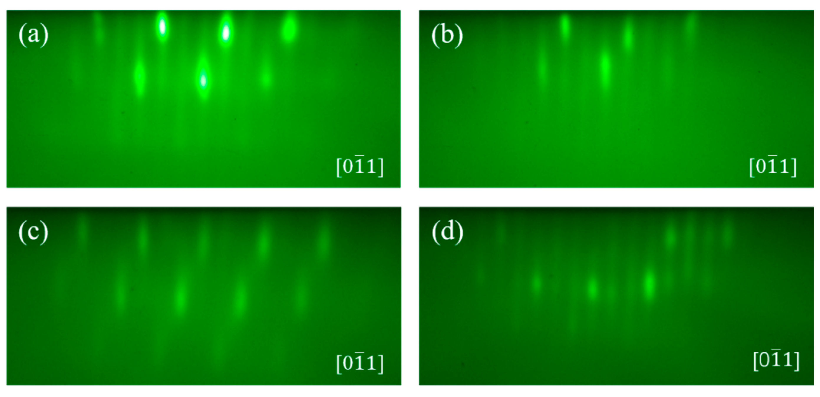
3.1. X-ray Diffraction

The X-ray diffraction (XRD) was used to characterize the crystal quality and orientation of the HgCdTe (211) film, as shown in Figure 2. The graphs for Sample 1 and Sample 2 have no obvious miscellaneous peaks, as shown in Figure 2a. The diffraction peaks at 71.4° and 83.5° correspond to the HgCdTe (422) and the GaAs (422). The Figure 2b shows the HgCdTe (422) XRD rocking curve FWHMs of Sample 1 and Sample 2, which are 179 and 128 arcsec, respectively. This indicates that the crystal quality of Sample 2 is better.

3.2. Scanning Electron Microscope

Figure 3a,b are the SEM images of the HgCdTe surface of Sample 1 and Sample 2. Figure 3a is the SEM image of Sample 1. The figure inset is an enlarged image of a surface defect. Larger voids will be formed on the surface at lower Hg flux or higher growth temperature (as shown in Figure 3a). The size of the voids depends on the degree of Hg deficiency [13]. As the degree of Hg deficiency becomes more serious, the Hg-deficiency gradually increases, and the size usually does not exceed 30 μm. Figure 3b shows the surface morphology of Sample 2 without Hg-deficiency. Obviously, the macroscopic defects of HgCdTe film grown at 151 °C are less than those of HgCdTe films grown at 155 °C. The surface quality of HgCdTe epilayer is very sensitive to the growth conditions owing to the low adhesion coefficient of Hg. Therefore, the growth temperature plays a crucial role in the surface quality of HgCdTe crystals under the condition of constant BEP ratio.

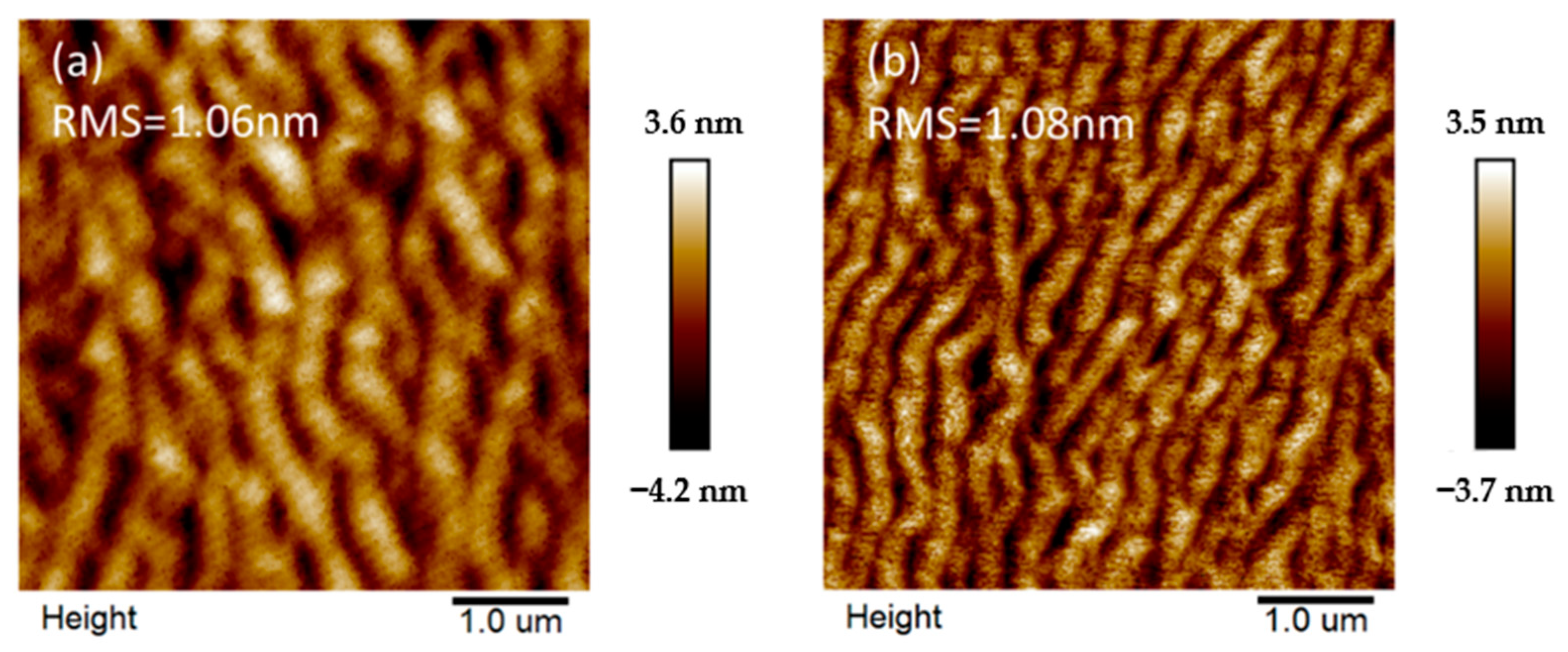
3.3. Atomic Force Microscopy

Figure 4 shows the AFM images of HgCdTe surface of Sample 1 (a) and Sample 2 (b). As can be seen from Figure 4, the roughness (RMS values) of both samples is less than 2 nm, indicating the smooth surface of the HgCdTe films. Meanwhile there are nano-ripples along the [1 1 ¯ 1] direction on the surface of the both samples, similar with the report [16]. The nano-ripples can be attributed to meandering macro step edges formed due to an instability in the step flow growth mode. Nano-ripples are affected by growth temperature and lattice mismatch between substrate and epilayer. The nano-ripple spacings of Sample 1 and Sample 2 are approximately 0.33 and 0.25 μm, respectively. The spacing between HgCdTe nano-ripples of Sample 1 (grown at 151 °C) is smaller than that of Sample 2 (grown at 155 °C) and the height is lower than that of Sample 2, indicating that the density of HgCdTe nano-ripples grown at 151 °C is higher than that of HgCdTe nano-ripples grown at 155°C. Nano-ripples morphology is affected by the availability of atoms on the surface [17]. The availability of surface atoms is closely related to growth conditions such as growth temperature, so the surface morphology under different growth conditions is different.

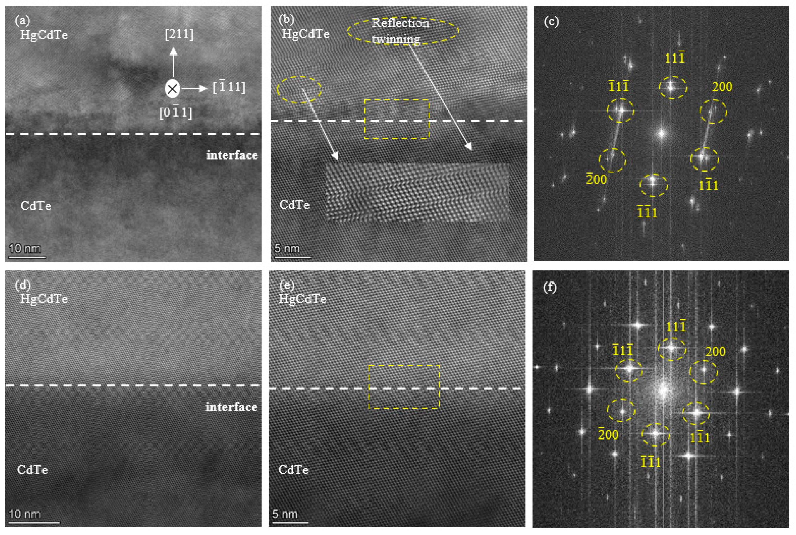
3.4. Scanning Transmission Electron Microscopy

The interface of the CdTe buffer layer and HgCdTe epilayer was characterized by scanning transmission electron microscopy (STEM), as shown in Figure 5a–c for Sample 1 and Figure 5d–f for Sample 2. As can be seen from Figure 5a, there is an obvious interface between the HgCdTe film grown at 155 °C and CdTe buffer layer. Figure 5d shows that there is no obvious interface between HgCdTe grown at 151 °C and CdTe, and no obvious twinning and stacking fault. Figure 5b,e shows the enlarged STEM images of Sample 1 and Sample 2, respectively. As can be seen from Figure 5b, lattice distortion occurs in the epilayer, and stacking fault can be found in the inset. The crystal lattices before and after stacking faults are symmetrical, indicating the presence of twins in the epilayer, while in Figure 5e, no reflection twinning can be seen. Figure 5c shows the fast Fourier transform (FFT) pattern at the interface between HgCdTe and CdTe of Sample 1. It can be seen that there are two diffraction lattices and the lattice is blurred, which indicates the existence of stacking faults and micro-twinning in the HgCdTe epilayer. Figure 5f shows the FFT pattern at the interface between HgCdTe and CdTe of Sample 2. The diffraction spots are clear and bright, indicating that no twinning and stacking faults were found in the HgCdTe layer grown at 151 °C. It shows that the crystal quality of the HgCdTe layer grown at 151 °C is better than that grown at 155 °C.
During crystal growth, the lattice mismatch between CdTe and HgCdTe leads to the formation of dislocation at the interface. At the same time, the formation of twinning is greatly affected by temperature. When the growth temperature is 151 °C, there is no large amount of micro-twinning in the HgCdTe layer at the interface, and the lattice quality at the interface is better. However, twinning appeared at the growth temperature of 155 °C. This due to the occurrence of Te-rich defects at high growth temperature, which leads to stacking faults and the formation of micro-twins.
In Figure 5b, the lamellar growth twins parallel to the (111) plane [18]. Micro-twins tend to appear along the [111] orientation because the surface energy of (111) plane is lower than that of (211) and (331) planes, so the dislocation is easier to migrate to (111) plane [19]. In general, the formation of twinning can be inhibited by the following methods: (1) The lattice matching between the epilayer and the substrate; (2) Adjust the growth direction of the epilayer (between [111] and [211]); (3) Optimize growth conditions to reduce twins, etc.

3.5. Raman Spectra

Figure 6 shows the Raman spectra of Sample 1 (a) and Sample 2 (b). Raman spectroscopy, which originates from molecular vibration and rotation, is sensitive to the structure, composition and defects of the material, and thus provides one of the main means of characterization for studying the lattice integrity, composition uniformity and crystal quality of the material. For the Sample 1, two defect peaks and three phonon features were observed which are located at 81, 107, 128, 140 and 153 cm−1. The peaks at 128 cm−1 and 140 cm−1 can be assigned to the HgTe-like transverse optical (TO) mode and longitudinal optical (LO) mode, the peak at 153 cm−1 can be assigned to the CdTe-like TO and LO mode. For the Sample 2, one defect peak and two phonon features were observed which are located at 87, 116, and 137 cm−1, and the peaks at 116 and 137 cm−1 is the HgTe-like TO and LO mode. The Raman peak positions and FWHMs of Sample 1 and Sample 2 as shown in Table 3. The peaks at 81 and 87 cm−1 are named D1, the peak at 107 cm−1 is named D2. Compared with Sample 2, the TO1 and LO1 peaks of Sample 1 shift to higher frequencies. Due to the stacking faults in Sample 1, the lattice distortion is caused, which leads to compressive stress inside the crystal.
As can be seen in Figure 6, D1 defect peaks are found in both Sample 1 and Sample 2, which is due to the lattice disorder of HgCdTe grown by MBE. Mazur [20] studied this peak and found that the peak disappeared after the annealing process. Annealing can improve the crystal quality and make the crystal lattice from disorder to order. The D2 defect peak in Sample 1 is related to Hg-deficiency, which has been previously explained in another article [21]. There are many Hg-deficiencies on the surface of Sample 1 (as shown in Figure 3a), so the peak related to Hg-deficiency can be detected by Raman spectra. It has been reported that low temperature annealing in Hg atmosphere can reduce Hg vacancies and thus eliminate the Raman peak of Hg vacancies. Moreover, there is a large number of Hg-deficiency in Sample 1, which causes lattice distortion. The shape and position of characteristic Raman peaks LO and TO are mainly related to lattice defects [22]. Therefore, the LO1 peaks of Sample 1 are not obvious, while the LO1 peaks of Sample 2 are obvious and symmetrical. As shown in Figure 6a, there are TO2/LO2 peaks for Sample 1, which may cause by the uneven surface composition caused by the Hg deficiencies.
The FWHM of the TO1 for HgCdTe Sample 1 and Sample 2 are 10.5 cm−1 and 16.2 cm−1, and the FWHM of LO1 for Sample 2 is 8.9 cm−1. Through the comparison of the Raman diagram, it can be seen that Sample 2 (grown at 151 °C) has fewer defects than Sample 1 (grown at 155 °C), and the crystal quality is better. The FWHMs of TO1 and LO1 of Sample 2 are similar to those of the other article [23].

3.6. Photoluminescence Spectroscopy

The photoluminescence (PL) is a nondestructive optical test method widely used to detect impurities, defects, and crystal quality of materials. Sample 1 and Sample 2 were subjected to variable temperature PL measurement and excited with a laser power of 100 mW, power density is 1.4 × 10⁵ mW/cm2. Figure 7a,b shows the normalized PL diagram of the samples. It can be seen from Figure 7a,b the PL peaks of the two samples blue-shifted and broadened with the increase in temperature, which is caused by the increase in Cd concentration. Both Sample 1 and Sample 2 have double peaks above 160 K, which is caused by CO2/H2O in the environment [24]. The asymmetry of the PL spectrum is mainly due to the thermal distribution effect of the high-temperature carrier. At 9 K, the FWHMs of Sample 1 and Sample 2 are 25.2 and 19.2 meV, respectively. The FWHMs of the PL of the Sample 2 are smaller than that of the Sample 1, which proves that the crystal quality of the Sample 2 is better than that of the Sample 1.
Figure 7c,d shows the temperature dependence of the main PL peak of the HgCdTe film. The solid line represents the relationship between Eg and temperature, while the data points represent test results. It can be seen from Figure 7c,d that the values of EgPL for Sample 1 and Sample 2 have a similar temperature coefficient (269 μeV/K and 275 μeV/K, respectively), which are higher than the Eg temperature coefficient of 195 μeV/K according to the calculation results of the formula 1. H.Wang et al. [25] have reported the similar results for LPE growth HgCdTe film. As PL transitions of HgCdTe film related to the excitonic effect and the band-tail of states at low temperatures present more evidently, and make the EgPL red-shift as compared to the Eg. Thus, the coefficient of EgPL and Eg of the HgCdTe film are quite different. From the variable temperature spectra, the activation energy ∆E of the HgCdTe Sample 1 and Sample 2 are 1.30 ± 0.14 and 0.75 ± 0.16 meV, respectively. Due to the absorption of the peak by CO2, the accurate result of the correlation of the peak intensity to 1/T is affected. The reason for small activation energy of the films is still under study.
As shown above, the HgCdTe film grown at 155 °C has many Hg-deficiencies and poor crystal quality. Additionally, there is micro-twinning along the [111] orientation at the HgCdTe/CdTe interface. The formation of micro-twinning caused by stacking faults formed by the Te-rich and the lattice mismatch between CdTe and HgCdTe. The HgCdTe film grown at 151 °C does not have a large number of defects and stacking faults at the HgCdTe/CdTe interface, and the crystal quality is better that of HgCdTe film grown at 155 °C. This shows that temperature has a significant effect on the crystal quality of HgCdTe thin films.

4. Conclusions

In this work, the single-crystal HgCdTe (211) films were successfully grown on GaAs (211) B substrates by MBE, and the effects of growth temperature on the crystal quality of HgCdTe/CdTe interface were studied. The HgCdTe film grown at 151 °C has high crystal quality, the interface is flat and there are no micro-twins. The crystal quality of the HgCdTe grown at 155 °C is poor, and there are many defects and micro-twins at the interface, which are caused by the high temperature-induced Te-rich defects. Raman peaks of HgCdTe with growth temperatures of 155 °C also demonstrate that the higher temperature would cause the lattice disorder of HgCdTe/CdTe interfaces. The research results demonstrate that the temperature significantly affects the crystal quality and optical properties of HgCdTe films.

Author Contributions

Data curation, X.-F.Q., S.-X.Z., J.Z., Y.-C.Z., C.D. and S.-C.H.; Formal analysis, X.-F.Q. and P.-P.C.; Funding acquisition, P.-P.C.; Methodology, X.-F.Q., S.-X.Z., J.Z., Y.W., S.-C.H. and P.-P.C.; Supervision, Y.W. and P.-P.C.; Validation, P.-P.C.; Writing—original draft, X.-F.Q.; Writing—review & editing, X.-F.Q. and P.-P.C. All authors have read and agreed to the published version of the manuscript.

Funding

This work was supported by the National Nature Science Foundation of China (Grant Nos. 11634009, 11991060, 11991063, 11774016).

Institutional Review Board Statement

Not applicable.

Informed Consent Statement

Not applicable.

Data Availability Statement

All data are fully available without restriction. The datasets used and/or analyzed during the current study are available from the corresponding author on reasonable request.

Acknowledgments

We acknowledge the financial support from the National Nature Science Foundation of China (Grant Nos. 11634009, 11991060, 11991063, 11774016) is gratefully acknowledged.

Conflicts of Interest

The authors declare no conflict of interest.

References

  1. Rogalski, A.; Razeghi, M. Narrow-gap semiconductor photodiodes. In Proceedings of the Photodetectors: Materials and Devices III, San Jose, CA, USA, 8 April 1998; Volume 3287, pp. 2–13. [Google Scholar]
  2. Hoang, A.M.; Dehzangi, A.; Adhikary, S.; Razeghi, M. High performance bias-selectable three-color Short-wave/Mid-wave/Long-wave Infrared Photodetectors based on Type-II InAs/GaSb/AlSb superlattices. Sci. Rep. 2016, 6, 24144. [Google Scholar] [CrossRef] [Green Version]
  3. Lei, W.; Antoszewski, J.; Faraone, L. Progress, challenges, and opportunities for HgCdTe infrared materials and detectors. Appl. Phys. Rev. 2015, 2, 41303. [Google Scholar] [CrossRef]
  4. Rogalski, A.; Martyniuk, P.; Kopytko, M. InAs/GaSb type-II superlattice infrared detectors: Future prospect. Appl. Phys. Rev. 2017, 4, 31304. [Google Scholar] [CrossRef]
  5. Lü, Y.Q.; Lu, X.; Lu, Z.X.; Li, M. Review of Antimonide Infrared Detector Development at Home and Abroad. Aero Weapon. 2020, 27, 1–12. [Google Scholar]
  6. Destéfanis, G.; Tribolet, P.; Vuillermet, M.; Lanfrey, D.B. MCT IR detectors in France. In Proceedings of the Infrared Technology and Applications XXXVII, Orlando, FL, USA, 20 May 2011; Volume 8012, p. 801235. [Google Scholar]
  7. Kinch, M.A. High-operating-temperature (HOT) detector requirements. Mater. Infrared Detect. 2001, 4454, 168–179. [Google Scholar]
  8. Perrais, G.; Gravrand, O.; Baylet, J.; Destefanis, G.; Rothman, J. Gain and dark current characteristics of planar HgCdTe avalanche photo diodes. J. Electron. Mater. 2007, 36, 963–970. [Google Scholar] [CrossRef]
  9. Rothman, J.; Perrais, G.; Destefanis, G.; Baylet, J.; Castelein, P.; Chamonal, J.-P. High performance characteristics in pin MW HgCdTe e-APDs. In Proceedings of the Infrared Technology and Applications XXXIII, Orlando, FL, USA, 14 May 2007; Volume 6542, p. 654219. [Google Scholar]
  10. Lei, W.; Gu, R.; Antoszewski, J.; Dell, J.; Faraone, L. GaSb: A new alternative substrate for epitaxial growth of HgCdTe. J. Electron. Mater. 2014, 43, 2788–2794. [Google Scholar] [CrossRef]
  11. Zhao, J.; Yang, Y.L.; Li, Y.H.; Song, L.Y.; Ji, R.B. The Study of MBE Molecule Beam Based on the Ensemble Theory. Infrared Technol. 2006, 28, 466–469. [Google Scholar]
  12. Chang, Y.; Zhao, J.; Abad, H.; Grein, C.H.; Sivananthan, S.; Aoki, T.; Smith, D.J. Performance and reproducibility enhancement of HgCdTe molecular beam epitaxy growth on CdZnTe substrates using interfacial HgTe/CdTe superlattice layers. Appl. Phys. Lett. 2005, 86, 131924. [Google Scholar] [CrossRef]
  13. He, L.; Wu, Y.; Chen, L. Composition control and surface defects of MBE-grown HgCdTe. J. Cryst. Growth 2001, 227, 677–682. [Google Scholar] [CrossRef]
  14. Lei, W.; Ren, Y.L.; Madni, I.; Faraone, L. Low dislocation density MBE process for CdTe-on-GaSb as an alternative substrate for HgCdTe growth. Infrared Phys. Technol. 2018, 92, 96–102. [Google Scholar] [CrossRef]
  15. Chu, J.H. Narrow Band Gap Semiconductor Physics; Science Press: Beijing, China, 2005; p. 933. [Google Scholar]
  16. Benson, J.D.; Almeida, L.A.; Carmody, M.W.; Edwall, D.D.; Markunas, J.K.; Jacobs, R.N.; Martinka, M.; Lee, U. Surface Structure of Molecular Beam Epitaxy (211) B HgCdTe. J. Electron. Mater. 2007, 36, 949–957. [Google Scholar] [CrossRef]
  17. Tejedor, P.; Šmilauer, P.; Roberts, C.; Joyce, B.A. Surface-morphology evolution during unstable homoepitaxial growth of GaAs (110). Phys. Rev. B 1999, 59, 2341–2345. [Google Scholar] [CrossRef]
  18. Lei, W.; Gu, R.; Antoszewski, J.; Dell, J.; Neusser, G.; Sieger, M.; Mizaikoff, B.; Faraone, L. MBE growth of mid-wave infrared HgCdTe layers on GaSb alternative substrates. J. Electron. Mater. 2015, 44, 3180–3187. [Google Scholar] [CrossRef]
  19. Yang, B.; Xin, Y.; Rujirawat, S.; Browning, N.D.; Sivananthan, S. Molecular beam epitaxial growth and structural properties of HgCdTe layers on CdTe (211) B/Si (211) substrates. J. Appl. Phys. 2000, 88, 115–119. [Google Scholar] [CrossRef]
  20. Mazur, Y.I.; Kriven, S.I.; Tarasov, G.G.; Shevchenko, N.V. Vibrational modes activated by structural disorder in FIR transmission of Hg1-x-yCdxMnyTe. Semicond. Sci. Technol. 1993, 8, 1187. [Google Scholar] [CrossRef]
  21. Huang, S.; Xia, C.; Zhang, P. Defect analysis in mercury cadmium telluride by Raman scattering. Spectrosc. Spectr. Anal. 2001, 21, 492–494. [Google Scholar]
  22. Singh, A.; Shukla, A.; Pal, R. Raman investigation of optical phonons in the ion implanted Hg1−xCdxTe. Opt. Mater. 2016, 57, 34–38. [Google Scholar] [CrossRef]
  23. Singh, A.; Pal, R.; Dhar, V.; Pant, S.C. Raman spectroscopic study of HgCdTe epilayers for infrared detector array fabrication. Infrared Phys. Technol. 2011, 54, 44–47. [Google Scholar] [CrossRef]
  24. Zhang, X.; Shao, J.; Chen, L.; Lu, X.; Guo, S.; He, L.; Chu, J. Infrared photoluminescence of arsenic-doped HgCdTe in a wide temperature range of up to 290 K. J. Appl. Phys. 2011, 110, 43503. [Google Scholar] [CrossRef]
  25. Wang, H.; Hong, J.; Yue, F.; Jing, C.; Chu, J. Optical homogeneity analysis of Hg1−xCdxTe epitaxial layers: How to circumvent the influence of impurity absorption bands? Infrared Phys. Technol. 2017, 82, 1–7. [Google Scholar] [CrossRef]
Figure 1. (a,c) RHEED images of the CdTe buffer for Sample 1 and Sample 2, and (b,d) RHEED images before the end of the growth for HgCdTe films (Sample 1 and Sample 2).
Crystals 11 00296 g001
Figure 2. The XRD curve for HgCdTe (422) of Sample 1 and Sample 2: (a) 2θ−ω results; (b) HgCdTe (422) XRD rocking curve of Sample 1 and Sample 2.
Crystals 11 00296 g002
Figure 3. SEM images of the HgCdTe thin films grown at different temperatures of (a) Sample 1 and the inset is an Hg-deficiency enlarged image; (b) Sample 2.
Crystals 11 00296 g003
Figure 4. Surface morphology of the HgCdTe (211) thin films grown at different temperatures of (a) Sample 1 and (b) Sample 2.
Crystals 11 00296 g004
Figure 5. STEM and FFT patterns of the HgCdTe/CdTe interface of Sample 1 (ac) and Sample 2 (df). (a,d) STEM cross-sectional images of Sample 1 and Sample 2, which show the interface situations are different. (b,e) Magnified STEM of Sample 1 and Sample 2. The FFT patterns of (c) Sample 1 and (f) Sample 2.
Crystals 11 00296 g005
Figure 6. Raman diagrams of Sample 1 (a) and Sample 2 (b).
Crystals 11 00296 g006
Figure 7. The variable temperature PL of Sample 1 (a) and Sample 2 (b). The temperature dependence of the main PL peak of Sample 1 (c) and Sample 2 (d).
Crystals 11 00296 g007
Table 1. Growth conditions of the HgCdTe films.
SampleComponent (x)Thickness (μm)Growth Temperature (°C)CdTe Buffer BEP (Torr)
CdTe BufferHgCdTe Layer
Sample 10.3103.402601553.51 × 10−7
Sample 20.2982.972601513.57 × 10−7
Table 2. Composition measured by FTIR/PL.
SampleFTIRPL
Sample 10.3100.309
Sample 20.2980.298
Table 3. Raman peak positions and FWHMs of Sample 1, Sample 2.
SampleD1 (cm−1)D2 (cm−1)HgTe-Like TO1 (cm−1)TO1 FWHM (cm−1)HgTe-Like LO1 (cm−1)LO1 FWHM (cm−1)CdTe-Like TO2/LO2 (cm−1)
Sample 18110712810.5140--153
Sample 287--11616.21378.9--
Publisher’s Note: MDPI stays neutral with regard to jurisdictional claims in published maps and institutional affiliations.

