Article

Gold Nanoisland Agglomeration upon the Substrate Assisted Chemical Etching Based on Thermal Annealing Process

by
Potejana Potejanasak
1,* and
Sethavut Duangchan
2
1
Department of Industrial Engineering, School of Engineering, University of Phayao, Phayao 56000, Thailand
2
Department of Industrial Physics and Medical Instrumentation, Faculty of Applied Science, King Mongkut’s University of Technology North Bangkok, Bangkok 10800, Thailand
*
Author to whom correspondence should be addressed.
Crystals 2020, 10(6), 533; https://doi.org/10.3390/cryst10060533
Submission received: 28 May 2020 / Revised: 16 June 2020 / Accepted: 20 June 2020 / Published: 23 June 2020
(This article belongs to the Special Issue Optical and Microstructural Characterization of Thin Layers)

Abstract

:
In this study, we proposed the self-organization process and its localized surface plasmon resonance property (LSPR) to study the effect of chemically treated quartz glass substrates for gold nanoisland array formation. Firstly, we etched a quartz glass substrate using a sputter etching machine. Secondly, n-butanol was treated on the surface of the substrate. Then, we deposited a gold thin film on the substrate with assisted chemical etching. Finally, the self-organization method examined the thermal annealing of gold nanoisland arrays on a substrate. The results showed that the gold nanoisland that was aggregated on an etched quartz glass substrate was large and sparse, while the gold nanoisland aggregated on a chemically treated substrate was small and dense. Further, it was revealed that a substrate’s surface energy reduced chemical treating and increased the gold nanoisland contact angle on the substrate via the thermal annealing process. It was also confirmed that chemical treatment was useful to control the morphology of gold nanoisland arrays on a substrate, particularly when related to tuning their optical property.

1. Introduction

It is known that metal nanoisland arrays exhibit unique optical properties, such as a localized surface plasmon resonance (LSPR). LSPR is attributed to the collective resonant oscillation of free electrons in metal nanostructures [1,2]. The vibration of the electromagnetic field of incident light excites it, thus causing a unique extinction spectrum that depends on the material and geometry of the metal nanostructures [3,4,5]. Since the peak wavelength of the extinction spectrum depends on the refractive index around the metal nanostructures, the nanoisland arrays can be utilized as a bimolecular optical plasmonic sensor to examine DNA, proteins, enzymes, and viruses [6,7,8,9]. The metallic nanoisland array biosensor enables us to detect biomolecules label-free, which is advantageous due to simplicity and short time detection [10,11,12].
Nanostructure patterns are generally fabricated by top-down fabrication methods, such as electron beam lithography [13,14,15], which focuses on ion beam milling [16,17,18] and nanoimprinting lithography [19,20]. These techniques are useful when fabricating well-defined and well-positioned metallic nanostructures such as nanowire arrays and nanoporous patterns on a hard substrate. However, these processes comprise complicated processes like resist coating, pattern drawing, and the lift-off process. In addition, they require stringent control of process conditions and costly equipment. Therefore, the throughput is low and production cost is high. In the meanwhile, bottom-up approaches like self-organization methods thermal dewetting [21,22,23,24,25] and anodic aluminum oxide (AAO) templates [26] enable us to fabricate metal nanoisland arrays and nanowire patterns by simple thermal dewetting or mask deposition processes. However, it is difficult to control the size and arrangement of the nanoisland arrays using only self-organization methods. In addition, the fabrication of porous alumina mask acidic electrolytes anodizing, which consists of complicated processes and requires stringent control.
The self-organization of thermal dewetting approaches requires less stringent process conditions and they are much simpler than conventional lithography methods. Therefore, they can achieve a lower cost and higher throughput production of nanodot devices. However, the configuration and size of the nanodots are difficult to control these self-organization methods. While thermal dewetting suffers the disadvantage of random dot size distribution, it offers the advantages of simplicity, low-cost, large-scale production, and high throughput. This technique is a general process to fabricate various metallic components and alloys. It is also easy to combine with other state-of-art lithographic techniques. For example, ordered arrays of faceted Au nanoparticles were synthesized by nanosphere lithography combined with a short annealing treatment [27].
In order to overcome these problems, two different approaches of (i) the substrate-assisted chemical etching and (ii) the etched substrate for thermal dewetting methods were experimentally studied. We developed the fabrication process of gold nanoisland arrays on a quartz glass substrate, which is based on chemically treated etching on the substrate during the thermal dewetting process. In this contribution, we experimentally study the influence of chemical treatments on the aggregation behavior of nanoisland arrays on substrates. We compare the two abovementioned approaches from the point of view of LSPR spectral measurements.

2. Materials and Methods

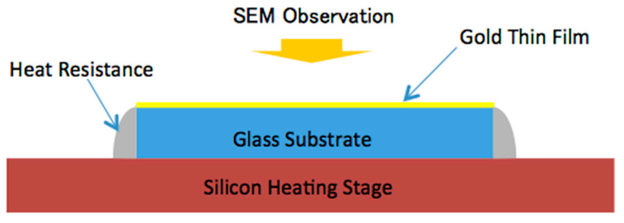
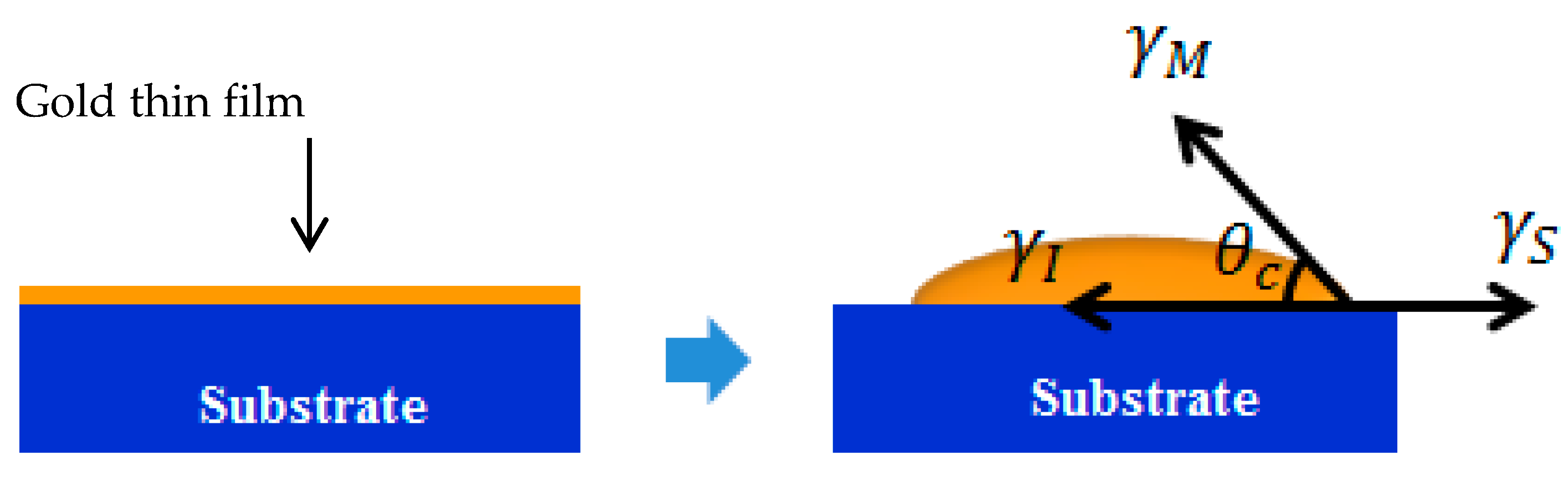
2.1. Thermal Annealing Method

Using the thermal annealing method for metal thin film offers a simple, low-cost, and high throughput fabrication technique to produce random nanostructures on a substrate. The evaporation and thermal annealing processes prepared the random gold island films. A continuous thin metal film was agglomerated into arrays of isolated islands, which minimized the system’s total interfacial energy when the metal film was heated to the adequate annealing temperatures. The mechanisms for a metal gold film were separated into metal islands and led to the agglomeration of gold nanodots on the substrate (Figure 1). Firstly, (a) dewetting metal films start from very small substrate holes. (b) During the annealing process, these holes continuously widen. (c) At the suitable annealing temperature and time, the void continuously expanded and separated the gold film into isolated islands. Finally, (d) the metal particles agglomerated on the substrate. The significant parameter for nanoparticle agglomeration on the substrate used thermal annealing methods, such as surface energy of metal thin film thickness, annealing temperature, and time. Thermal annealing methods suffered the drawback of random metal nanoparticle size distribution, offering the advantages of simplicity processed with low-cost and high fabrication throughput [28,29,30,31].

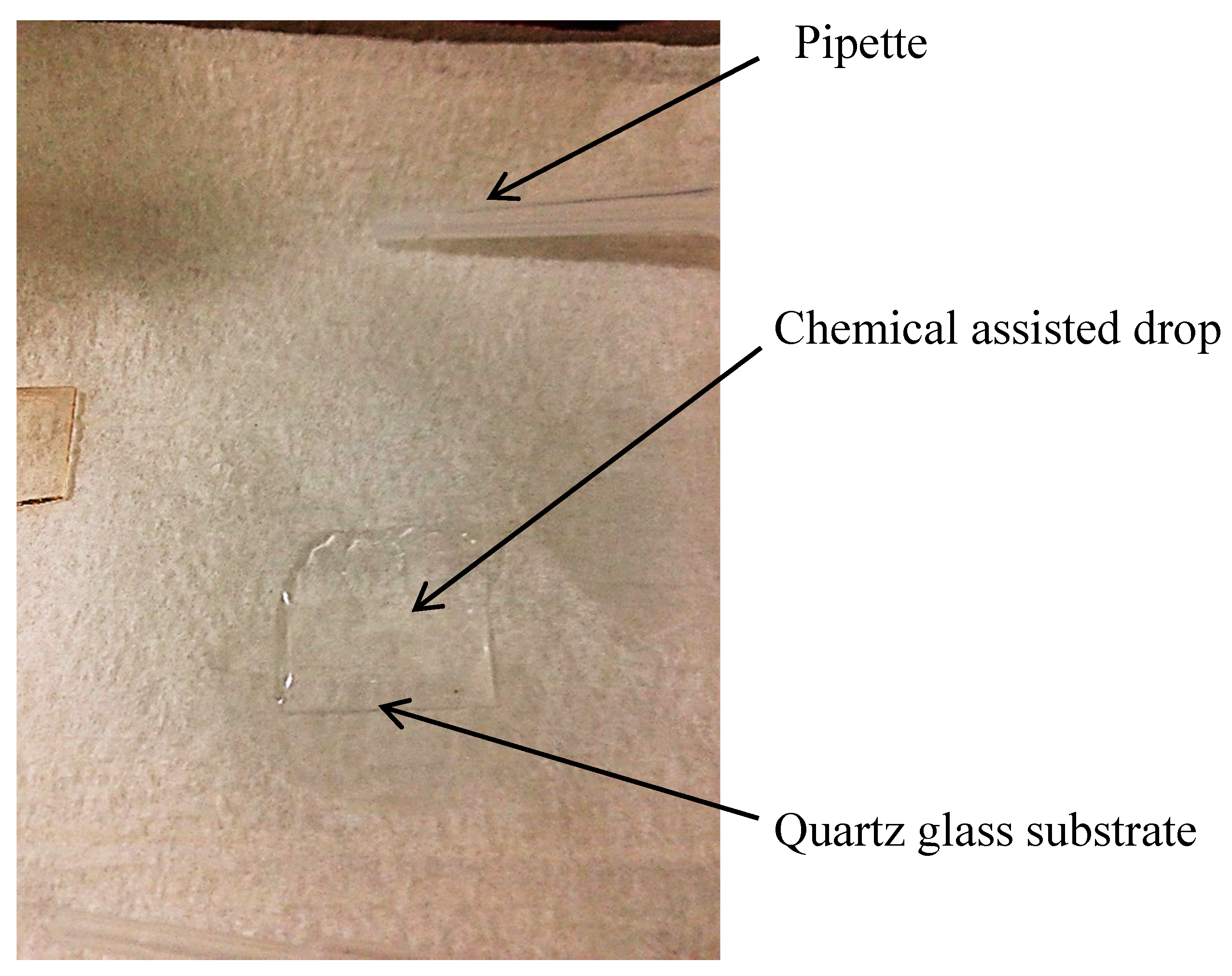
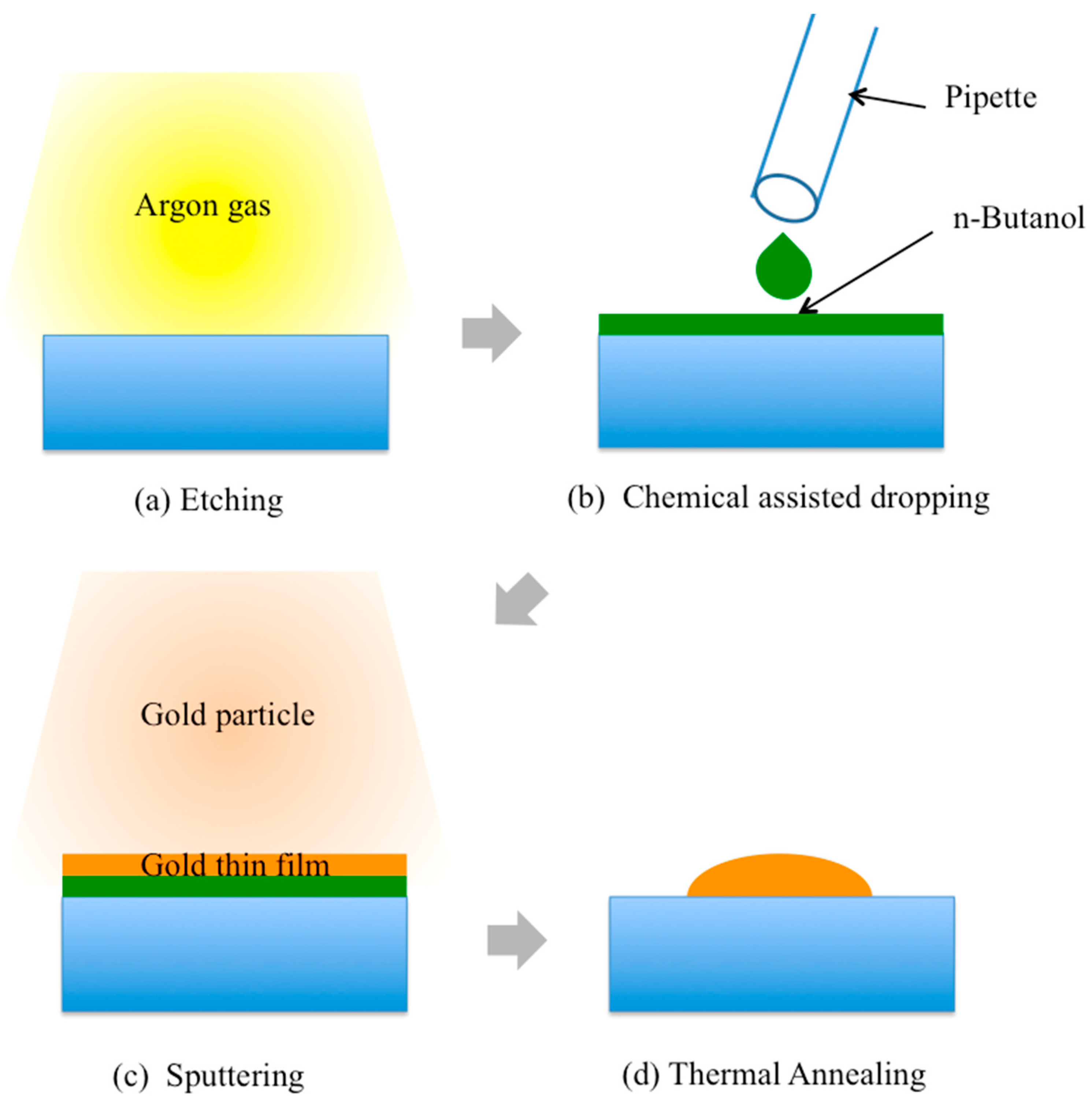
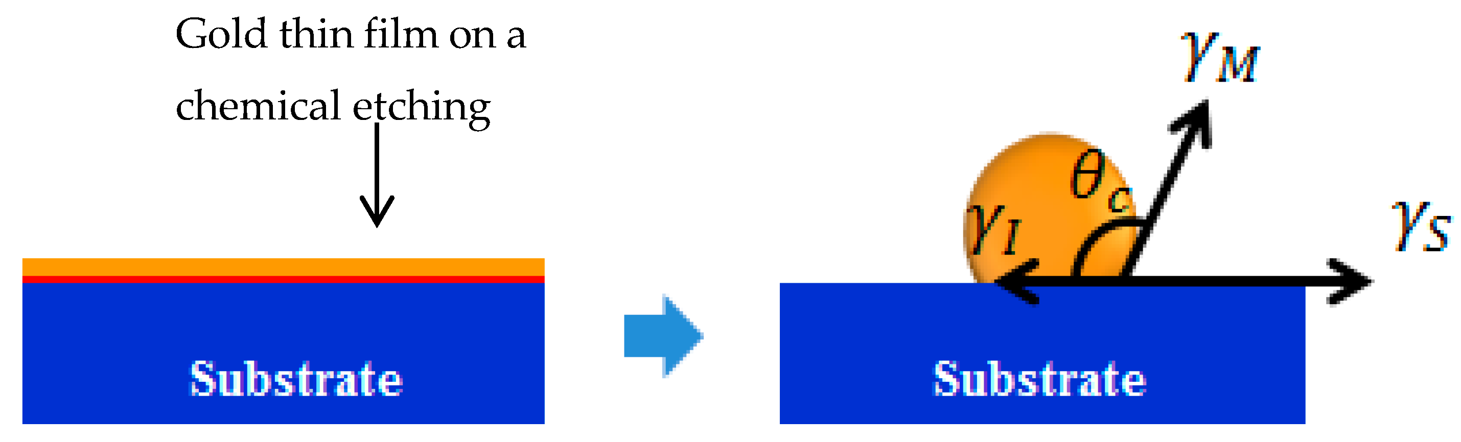
2.2. The Substrate-Assisted Chemical Etching Based on the Thermal Annealing Process
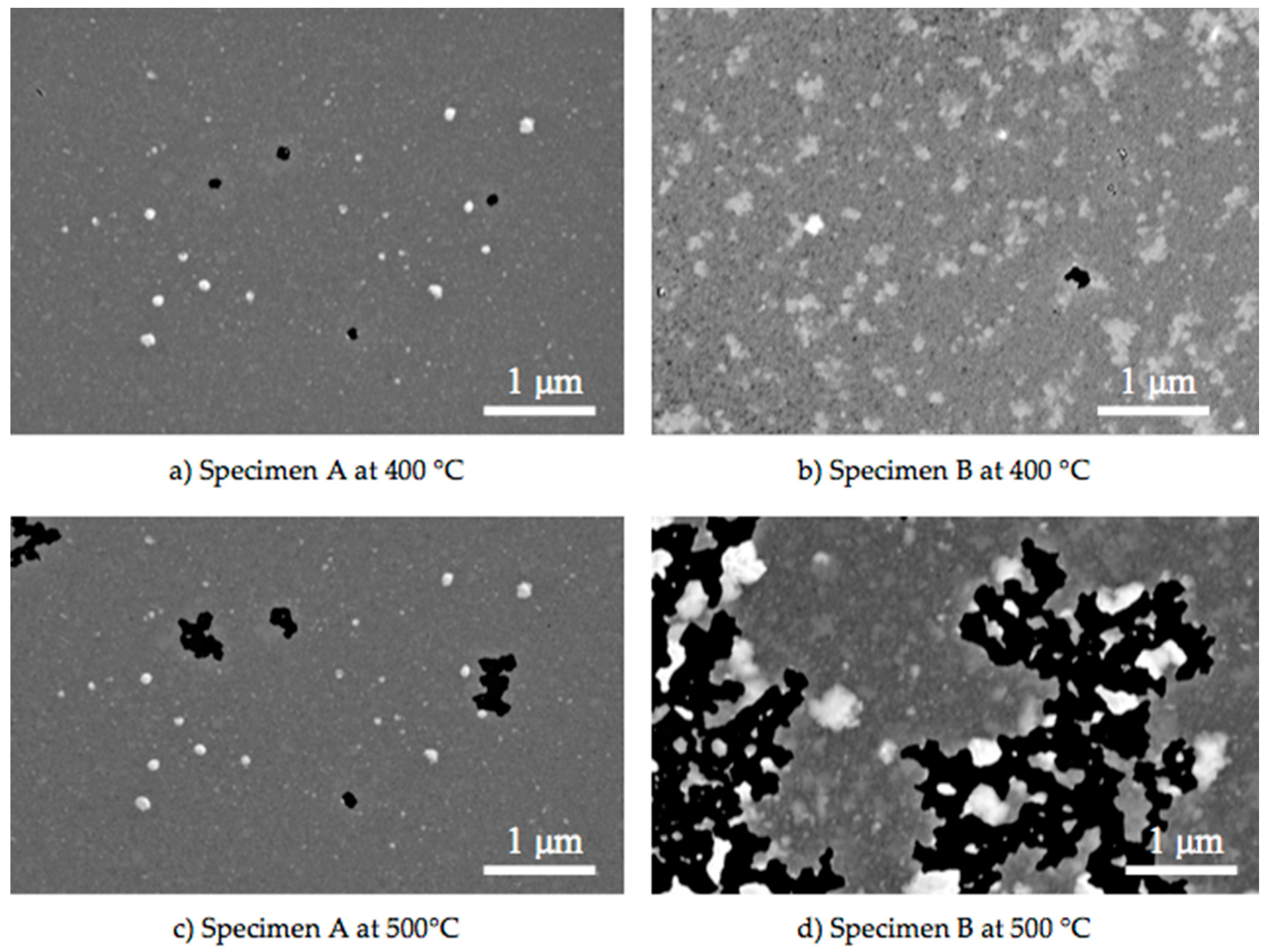
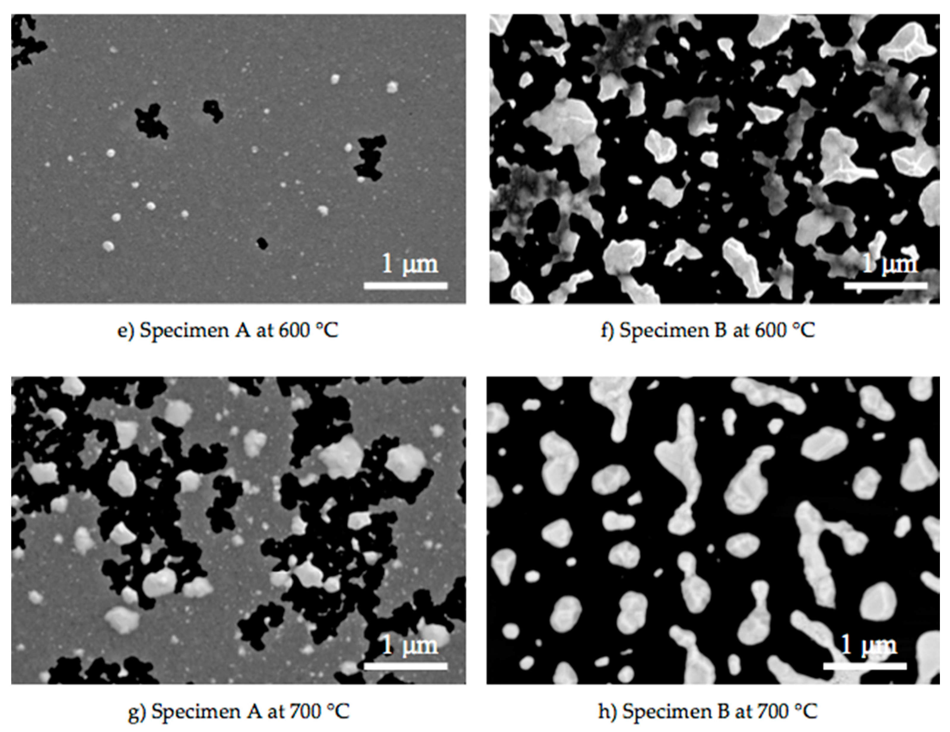
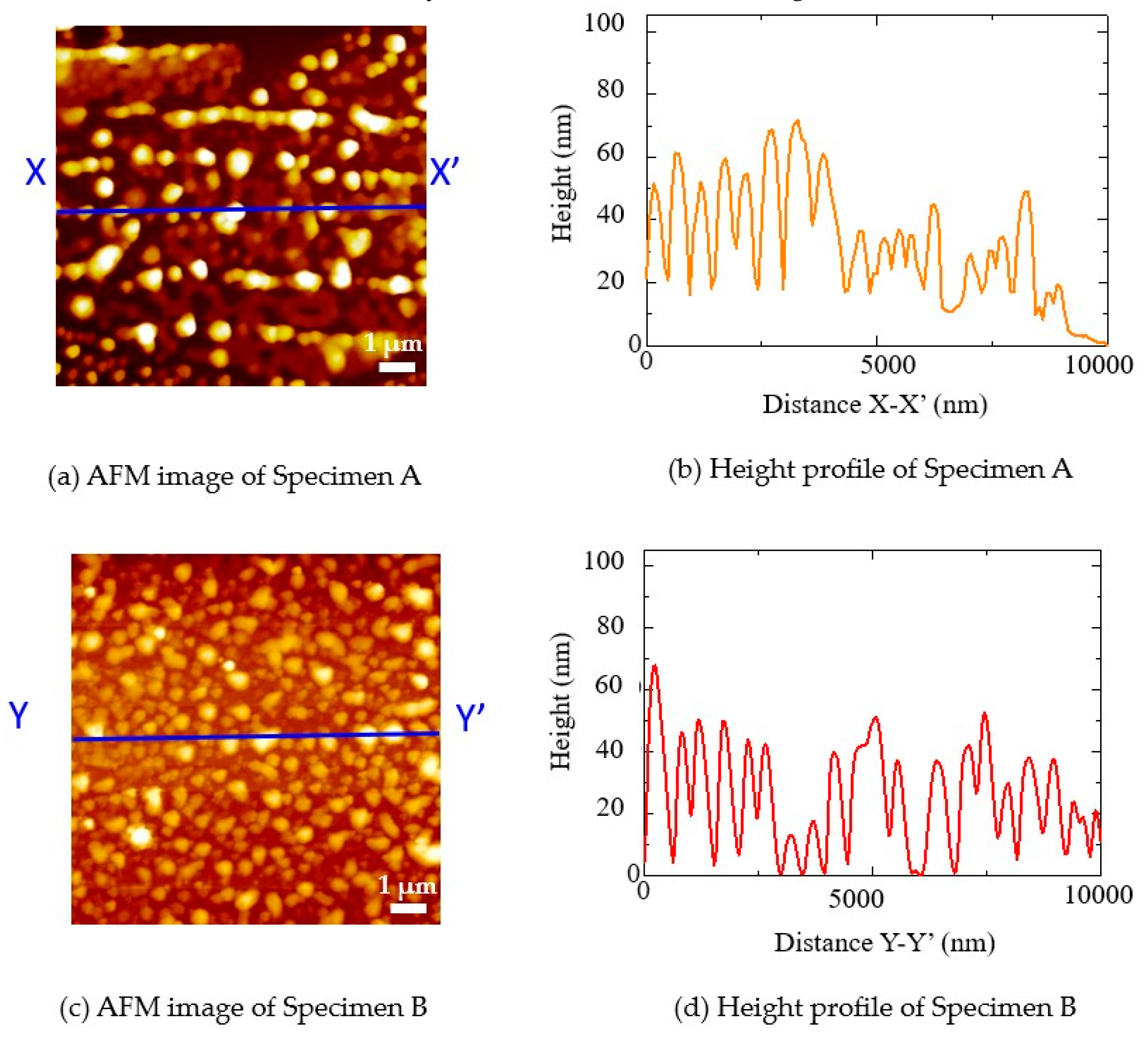
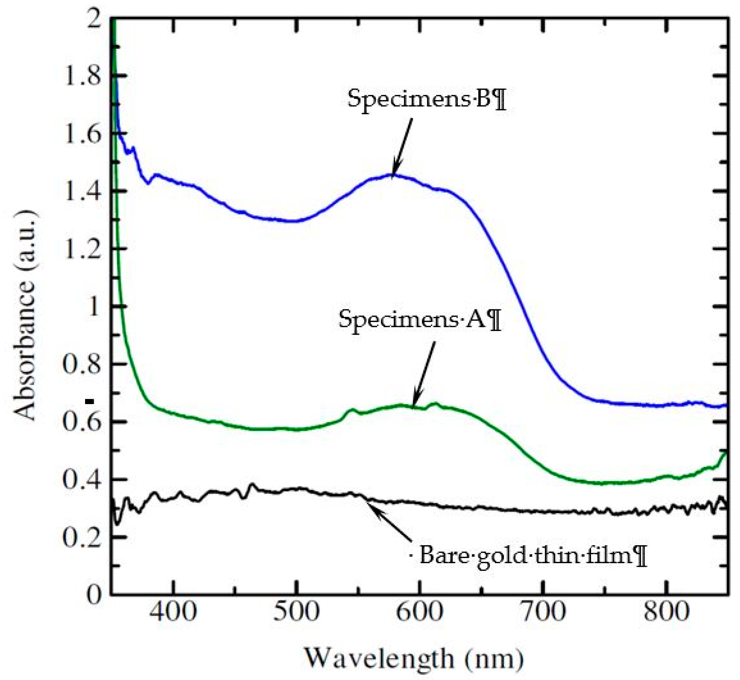
We examined the effect of chemical treatments on the morphology of gold nanoislands fabricated by thermal dewetting. A quartz glass substrate 1 mm thick was cut to be 10 mm × 10 mm (Figure 2). It was cleaned by an ultrasonic cleaner in an acetone bath for 15 min. (a) The substrates were etched with Ar+ gas for 2 min under a pressure of 15 Pa. The distance between the substrate and Au target was 35 mm, the acceleration voltage was 0.7 kV, and the sputter current was maintained at 5 mA during the sputter etching process by using the sputter coater machine. (b) Then, n-butanol was dropped on the substrates. The volume of the chemical drop was about 0.0274 mL by using a pipette (Figure 3). The dropped chemical was spread over the surface of the substrate and dried for 2 min in a clean room. (c) Then, Au film was deposited on the substrates for 10 nm of thickness by a sputter coater. (d) Finally, the substrates were annealed in an electric furnace at 700 °C for 15 min when dot agglomeration via thermal dewetting occurred. In this study, we experimentally examined the two differences treated on glass substrates: specimen A, the etched substrate, without step (b), and specimen B: the substrate-assisted N-Butanol etching. Nanoisland array morphology was characterized using a field emission scanning electron microscope, (FE-SEM, Hitachi SU3500, Japan).
The Gatan Murano hot stage characterized the dynamic observation of a gold nanoisland array agglomeration on a glass substrate. The Silicon type hot stage was mounted inside the standard scanning electron microscope (FE-SEM, Hitachi SU3500, Japan). Figure 4 shows the schematic diagram of the substrate on the silicon heating stage, which allowed for direct observation of agglomeration behavior for simulated thermal treatment during the annealing process. The stage temperatures range spanned from ambient to 700 °C.
The LSPR extinction spectrum for nanoisland arrays on a glass substrate was analyzed using a transmission ultraviolet-visible (UV-VIS) spectrometer, SEC2000-VIS/NIR spectrometer (ALS Co., Ltd, Japan). The measured spot size was about 0.5 mm in diameter. The UV-Vis light by Tungsten and Halogen light source (LS-1, Ocean Optics, ALS Co., Ltd, Japan) was passed through the gold nanoisland arrays and the absorbance spectra of light by the nanoisland arrays was measured. The absorbance spectrum was measured by giving wavelengths in between the visible range of 200–800 nm.

3. Results

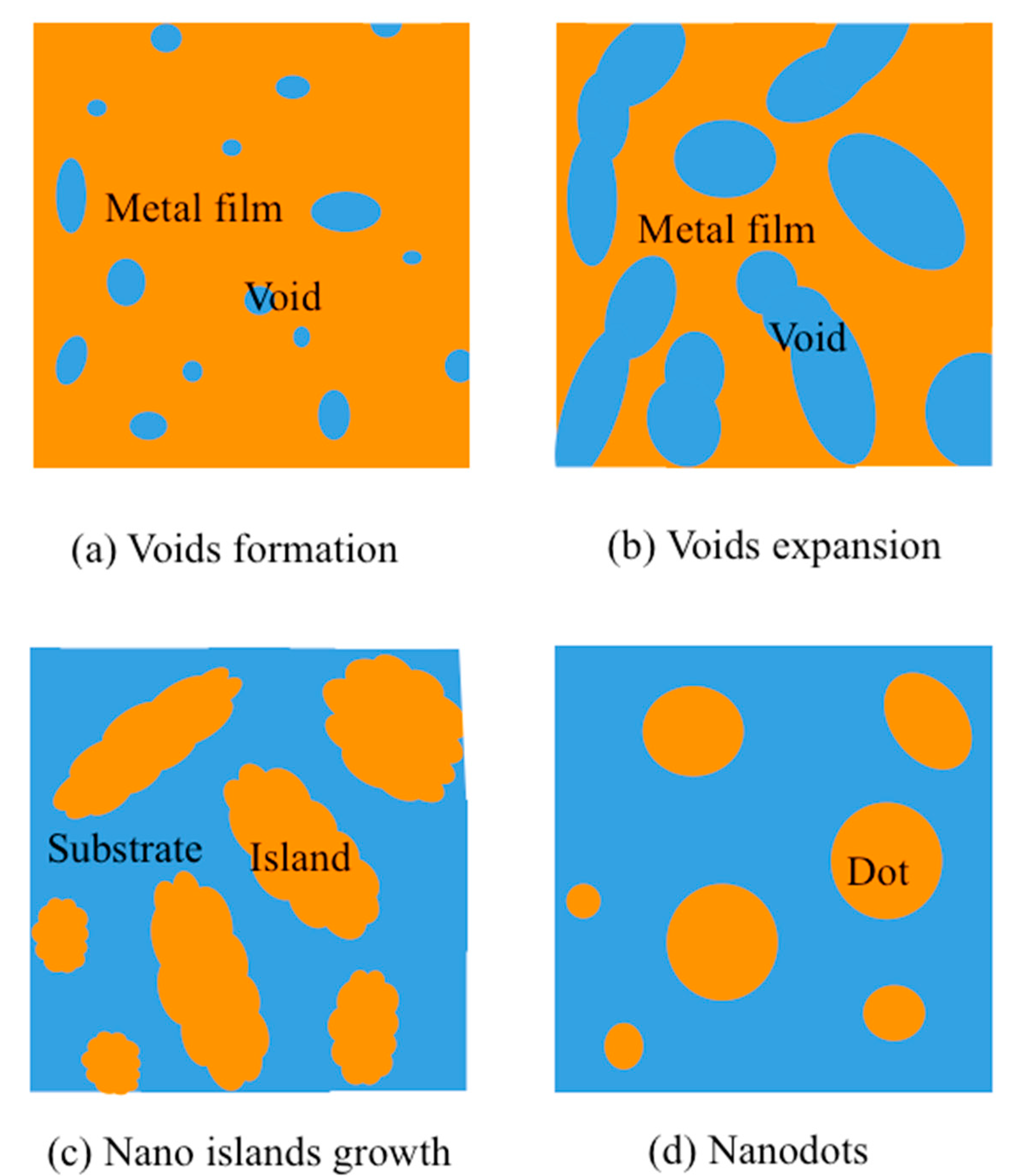
A Comparison of the Agglomeration Process for Gold Nanoislands on the Substarte

The LSPR extinction spectrum of the nanoisland arrays on a glass substrate was analyzed using a transmission ultraviolet-visible (UV-VIS) spectrometer, SEC2000-VIS/NIR spectrometer. The measured spot size was about 0.5 mm in diameter. The UV-Vis light by Tungsten and Halogen light source (LS-1, Ocean Optics) was passed through the nanoisland arrays and the absorbance spectra of light by the nanoisland arrays was measured. The absorbance spectrum was measured by giving a wavelength in between the visible range of 200–800 nm. The influence of chemically etching a glass substrate on the morphology of nanoislands was experimentally studied by carrying out annealing during the hot stage via FE-SEM. Figure 4 illustrates FE-SEM micrographs to compare the agglomeration evolution of random gold nanoisland arrays on specimens A and B. Figure 5a illustrates the beginning stage of a gold thin film on the surface of specimen A at 400 °C. It was found that many voids were exhibited on the gold thin film. Figure 5b shows the beginning stage of a gold thin film on the surface of specimen B at 400 °C. It was found that many small voids and chemically dried strains appeared on the gold thin film. When induced by the silicon heating stage at 500 °C (as shown in Figure 5c,d), the voids in the gold thin film of specimen B dramatically became larger than specimen A. In addition, specimen B’s sputtered gold thin film aggregated into larger nanoislands with different shapes at 600 °C (Figure 5f). By contrast, the gold thin film of specimen A was still the same as the previous specimen, as shown in Figure 5e. At the suitable heating temperature of 700 °C for 30 min, the void continuously expanded and the gold film agglomerated into nanoislands (Figure 5h). In other words, the gold thin film of specimen A gradually expanded into larger voids. This comparison justified our efforts of adopting an assisted n-butanol etching on the substrate before the thermal annealing processes in order to achieve faster agglomeration behavior and better uniformity of gold nanoisland arrays.
Figure 6a presents the Atomic Force Microscopy (AFM) image and the height profile of gold nanoislands on the etched substrate of specimen A for thermal annealing at 700 °C for 30 min. The incomplete agglomeration of gold nanoislands with uplift from a gold thin film appeared on the substrate’s surface. The average height of specimen A’s gold nanoisland, along with the X-X’ line, was approximately 27 nm (Figure 6b). On the other hand, Figure 6c illustrates the AFM image and the height profile of the gold nanoisland on specimen B’s assisted N-butanol etching for thermal annealing at 700 °C for 30 min. The gold thin film was agglomerated into many nanoislands via the thermal mechanism. The average height of specimen B’s gold nanoisland, along with the Y-Y’ line, was approximately 48 nm (Figure 6d). The result occurred because the gold thin film completely agglomerated into the nanoisland arrays, which increased their height.
FE-SEM micrographs determined the average contact angle for the gold nanoisland at 700 °C during thermal annealing (Figure 5(GHz)) and using ImageJ analysis software. For specimen A, the contact angle of gold nanoislands aggregated on the etched substrate was 78°. The contact angle of gold nanodots aggregated on the n-butanol assisted substrate as specimen B is 109°. It is confirmed that the contact angle of gold nanoislands on the n-butanol assisted substrate was larger than the etched substrate.

4. Discussions

The effect of chemical treatment on the gold nanoisland arrays was attributed to the contamination of chemical molecules on the substrates. According to the mathematical model presented in Young’s equation [32], we can see that:
γ I γ S = γ M cos θ c
where θ c is the contact angle at the equilibrium state. θ c is the surface energy of substrate γ S , surface energy of the metal dot γ M , and interfacial energy γ I between the metal and substrate. Thus, θ c was determined by combining materials used for the dot and substrate. The surface energy of the gold γ M was about 1000 mJ/m2 [33] and that of the quartz glass was about 220 mJ/m2 in room temperature [34]. However, the contamination of substrate surface influenced the surface energy of substrate and the interfacial energy.
In order to compare the agglomeration behavior at 700 °C between the gold nanoisland on a substrate between specimen A (Figure 5g) and specimen B (Figure 5g), acetone bath cleaning was conducted to remove oils and fats. However, acetone molecules remained on the surface of the quartz substrates even after acetone dried completely [35]. Thus, Ar sputter etching was subjected to the substrates to remove acetone molecules from the substrate surface. The heavy Ar+ ions were more effective for chipping away at the surface. An electrical discharge was created in a vacuum chamber by applying a voltage to a platen where the glass sat. Ar+ ions were pulled onto the platen and wafer with energy (in electron volts) similar to the applied voltage (0.7kV). The ion impact may setup a series of collisions between atoms in the target, which might lead to the ejection of some of these atoms (H2O and some of SiO2 on the surface of glass) [36]. Since the Ar sputtering broke bonding between acetone molecules and substrate atoms, the surface atoms were excited and the surface energy of the substrate ( γ S ) increased. This indicates that the contact angle θ c decreased because the left term of Equation (1) decreased (Figure 7). We confirmed that the gold thin film on the etched substrate was rather difficult to agglomerate the gold nanoisland arrays.
On the other hand, as for the chemically treated substrates, molecules of dropped n-butanol were adhered to the substrate surface. These molecules remained on the substrate after the n-butanol drop was dried [37]. Thus, the Au film was coated on the molecule layer, as illustrated in Figure 8. When this substrate was annealed, the gold thin film easily agglomerated to the substrate’s gold nanoisland array. However, the adhered chemical molecules influenced it. Since the adhered molecules reduced surface energy of the substrate ( γ S ), the left term of Equation (1) increased and the contact angle θ c also increased. We found that the gold thin film on a chemical etching glass substrate rather easily agglomerated to the gold nanoisland arrays.
Figure 9 shows the LSPR properties of fabricated nanoisland arrays on the glass substrate at 700 °C for 30 min. As shown by the figure, the clear peaks were observed in the visible light region. The absorbance spectra of the gold nanoislands on the etched substrate (specimen A) were flat and the peak was 600 nm. However, the absorbance spectra of the gold nanoislands on the n-butanol treated substrate (specimen B) were higher and steeper when it reached 570 nm. It was also confirmed that the intensity of the absorbance peak for specimen B was higher than for specimen A. This can be attributed to the morphology of nanoislands on the substrates. As shown in Figure 5h, the complete agglomeration of gold nanoislands for specimen B were generated, yet the distorted nanoislands were generated on the substrate of specimen A (Figure 5g). It was reported that the nanoislands’ uniform shape made for a narrower absorbance spectra peak. From the results, it is clearly shown that LSPR was very sensitive to dot morphology and distribution. It was also confirmed that the assisted chemical etching glass substrate with the gold thin film coated for the thermal annealing process could control the optical property of the gold nanoisland arrays.

5. Conclusions

This study demonstrates a simple low-cost with high throughput approach to fabricate plasmonic nanoisland arrays using Argon etching with chemical treating for the thermal annealing on quartz glass substrates. This study conditions were clarified to produce nanoislands with various dimensions for plasmonic sensing applications. On the basis of these results, as for the substrate-assisted n-butanol etching, molecules of the dropped chemicals adhered on the substrate surface. Thus, the gold thin film was deposited onto the n-butanol dried layer for thermal annealing. We found that the gold thin film on an assisted-chemical etching glass substrate was rather easily agglomerated to the gold nanoisland arrays, compared with only the etched substrate. The results discussed in this study indicated that the adhered n-butanol molecules on a surface of quartz glass substrate influenced the good uniformity of the gold nanoisland arrays. The adhered n-butanol molecules reduced the surface energy on the surface of a substrate related to control the contact angle in the agglomeration of the thermal annealing process. We also confirmed that the good uniformity of the gold nanoisland arrays on the substrate-assisted n-butanol etching was significant to control the LSPR optical properties. Overall, the gold nanoisland films by the substrate-assisted n-butanol etching method should be used for the fabrication of LSPR substrates.

Author Contributions

Conceptualization and methodology, P.P.; investigation, P.P. and S.D.; writing—original draft preparation, P.P. and S.D.; writing—review and editing, P.P.; visualization, P.P.; supervision, P.P.; project administration, P.P.; funding acquisition, P.P. All authors have read and agreed to the published version of the manuscript.

Funding

This research was funded by School of Engineering, University of Phayao.

Acknowledgments

This work was supported by the School of engineering, University of Phayao.

Conflicts of Interest

The authors declare no conflict of interest.

References

  1. Yue, B.Z.; Brian, K.; Paul, S.W.; Tony, J.H. Molecular plasmonics for biology and nanomedicine. Nanomedicine 2012, 7, 751–770. [Google Scholar]
  2. Hao, M.C.; Ru-Shi, L. 2011 Architecture of metallic nanostructures: Synthesis strategy and specific applications. J. Phys. Chem. C. 2011, 115, 3513–3527. [Google Scholar]
  3. Sagadevan, S. Semiconductor Nanomaterials, methods and applications: A review. J. Nanosci. Nanotechnol. 2013, 3, 62–74. [Google Scholar]
  4. Isao, M. 2005 Nanoparticles for electronic device application: A brief review. J. Chem. Eng. Jpn. 2005, 38, 535–546. [Google Scholar]
  5. Chia, W.H.; Bo, Z.; Wenjun, Q.; Ofer, S.; Brendan, G.D.; John, D.J.; Marin, S. Transparent displays enabled by resonant nanoparticle scattering. Nat. Commun. 2014, 5, 3152. [Google Scholar]
  6. Lan, Z.; Simone, P.; Giuliocesare, C.B.; Rakesh, M.; Pierre, M.A.; Marisa, M.; Rodica, E.I. Robust SERS platforms based on annealed gold nanostructures formed on ultrafine glass substrates for various (bio) applications. Biosensors 2019, 9, 53. [Google Scholar] [CrossRef] [Green Version]
  7. Thi, M.L.N.; Pham, V.T.; Bui, Q.B.; Ai-Le, P.H.; Nhac-Vu, H.-T. Novel nanohybrid of blackberry-like gold structures deposited graphene as a free-standing sensor for effective hydrogen peroxide detection. J. Solid State Chem. 2020, 286, 121299. [Google Scholar] [CrossRef]
  8. Longhua, G.; Joshua, A.J.; Huang, H.Y.; Peng, C.; Nam, J.C.; Dong, H.K. Strategies for enhancing the sensitivity of plasmonic nanosensors. Nano Today 2015, 10, 213–239. [Google Scholar]
  9. Jingwei, S.; Yuexiang, L.; Liuying, H.; Jiawei, P.; Fengyi, Y.; Yueying, L. A colorimetric sensor array for protein discrimination based on carbon nanodots-induced reversible aggregation of AuNP with GSH as a regulator. Sens. Actuators B Chem. 2019, 296, 126677. [Google Scholar]
  10. Wanbo, L.; Li, Z.; Jianhua, Z.; Hongkai, W. Well-designed metal nanostructured arrays for label-free plasmonic biosensing. J. Mater. Chem. C 2015, 3, 6479–6492. [Google Scholar]
  11. Hwang, C.S.H.; Ahn, M.; Lee, Y.; Taerin, C.; Ki, H.J. Ag/Au Alloyed Nanoislands for Wafer-Level Plasmonic Color Filter Arrays. Sci. Rep. 2019, 9, 9082. [Google Scholar] [CrossRef] [PubMed]
  12. Heesang, A.; Hyerin, S.; Jong-ryul, C.; Kyujung, K. A Localized Surface Plasmon Resonance Sensor Using Double-Metal-Complex Nanostructures and a Review of Recent Approaches. Sensors 2018, 18, 98. [Google Scholar]
  13. Luis, G.R.; Robert, F.P.; Steven, K.D.; Maria, S. Application of EBL fabricated nanostructured substrates for surface enhanced Raman spectroscopy detection of protein A in aqueous solution. J. Vac. Sci. Technol. 2013, 31, 06F901. [Google Scholar]
  14. Gwanho, Y.; Inki, K.; Sunae, S.; Jungho, M.; Minkyung, K.; Junsuk, R. Fabrication of three-dimensional suspended, interlayered and hierarchical nanostructures by accuracy-improved electron beam lithography overlay. Sci. Rep. 2017, 7, 6668. [Google Scholar]
  15. Anant, A.; Joseph, M.; Kathleen, A.C.; Tzanko, S. Electron-Beam-Lithographed Nanostructures as Reference Materials for Label-Free Scattered-Light Biosensing of Single Filoviruses. Sensors 2018, 18, 1670. [Google Scholar]
  16. Sarah, F.; Jerome, T.M.; Marija, D. Materials analysis and focused ion beam nanofabrication of topological insulator Bi2Se3. Sci. Rep. 2017, 7, 13466. [Google Scholar]
  17. Yang, L.; Helen, E.K.; Marijn, A.V.H.; Martyn, R.D.; Oliver, P. Nano-tomography of porous geological materials using focused ion beam-scanning electron microscopy. Minerals 2016, 6, 104. [Google Scholar]
  18. Xiaoyu, C.; Yuyu, X.; Yifei, M.; Yun, H.; Jia, Z.; Jun, X.; Rui, Z.; Lei, S.; Wengang, W. A Programmable nanofabrication method for complex 3D meta-atom array based on focused-ion-beam stress-induced deformation effect. Micromachines 2020, 11, 95. [Google Scholar]
  19. Grégory, B. Plasmonic nanostructures prepared by soft UV nanoimprint lithography and their application in biological sensing. Micromachines 2012, 3, 21–27. [Google Scholar]
  20. Cosmin, F.; Daniel, M.; Alia, C.; Ioana, B.; Lucian, B.T. Gold Nanopost-Shell Arrays Fabricated by Nanoimprint Lithography as a Flexible Plasmonic Sensing Platform. Nanomaterials 2019, 9, 1519. [Google Scholar]
  21. Tanya, K.; Alexander, B.T.; Takumi, S.; Yishay, F.; Alexander, V.; Israel, R. Mechanism of morphology transformation during annealing of nanostructured gold films on glass. Phys. Chem. Chem. Phys. 2013, 15, 4656. [Google Scholar]
  22. Andrzej, S.; Joanna, P.; Wojciech, M.; Regina, P. Nanostructuring of Si substrates by a metal- assisted chemical etching and dewetting process. RSC Adv. 2018, 8, 31224. [Google Scholar]
  23. Xin, S.; Hao, L. Gold nanoisland arrays by repeated deposition and post-deposition annealing for surface-enhanced Raman spectroscopy. Nanotechnology 2013, 24, 355706. [Google Scholar]
  24. Marco, A.; Nhat, T.N.; Patrik, S. Templated dewetting: Designing entirely self- organized platforms for photocatalysis. Chem. Sci. 2016, 7, 6865. [Google Scholar]
  25. José, M.M.M.d.A.; Helena, V.; Pedro, A.S.J.; Luis, C. Plasmonic optical fiber sensor based on double step growth of gold nano-islands. Sensors 2018, 18, 1267. [Google Scholar]
  26. Bo, C.Z.; Jen, B.S.; Hsien, S.L.; Po, Y.H.; Hsuan, W.L.; Chih, H.L.; Ming, W.L.; Ming, C.K. Growth of less than 20 nm SnO nanowires using an Anodic Aluminum Oxide template for gas sensing. Micromachines 2020, 11, 153. [Google Scholar]
  27. Adam, K.; Witold, K.; Hanna, G.; Michael, G. Fabrication of Nanoscale Rings, Dots, and Rods by Combining Shadow Nanosphere Lithography and Annealed Polystyrene Nanosphere Masks. Small 2015, 1, 439–444. [Google Scholar]
  28. Gupta, G.; Tanaka, D.; Ito, Y.; Shibata, D.; Shimojo, M.; Furuya, K.; Mitui, K.; Kajikawa, K. Absorption spectroscopy of gold nanoislands films: Optical and structural characterization. Nanotechnology 2009, 20, 025703. [Google Scholar] [CrossRef]
  29. Alena, R.; Zdenka, N.; Nikola, S.K.; Vaclav, S. Gold nanoparticles deposited on glass: Physicochemical characterization and cytocompatibility. Nanoscale Res. Lett. 2013, 8, 252. [Google Scholar] [CrossRef] [Green Version]
  30. Christian, W.; Wolfgang, W.; Michael, K.; Christian, R. Gold nano-particles fixed on glass. Appl. Surf. Sci. 2012, 258, 8503–8513. [Google Scholar]
  31. Svorcik, V.; Kvitek, O.; Riha, J.; Kolska, Z.; Siegel, J. Nano-structuring of sputtered gold layer on glass by annealing. Vacuum 2012, 86, 729–732. [Google Scholar] [CrossRef]
  32. Young, T. An essay on the cohesion of fluids. Philos. Trans. R. Soc. Lond. 1805, 95, 65–87. [Google Scholar]
  33. Vitos, L.; Ruban, A.V.; Skriver, H.L.; Kollar, J. The surface energy of metals. Surf. Sci. 1998, 411, 186–202. [Google Scholar] [CrossRef]
  34. Parks, G.A. Surface and interfacial free energies of quartz. J. Geophys. Res. 1984, 89, 3997–4008. [Google Scholar] [CrossRef]
  35. MacManus, J.C.; Harano, Y.; Low, A.M.D. Infrared study of the interactions of acetone and siliceous surfaces. Can. J. Chem. 1969, 47, 2545–2554. [Google Scholar] [CrossRef]
  36. Plummer, J.D.; Deal, M.D.; Griffin, P.B. Silicon VLSI Technology, Fundamentals, Practice and Modeling; Prentice Hall: Upper Saddle River, NJ, USA, 2000. [Google Scholar]
  37. Liu, W.; Liu, W.; Wang, X.; Wei, D.; Zhang, H.; Liu, W. Effect of butanol on flotation separation of quartz from hematite with N-dodecyl ethylenediamine. Int. J. Min. Sci. Technol. 2016, 26, 1059–1063. [Google Scholar] [CrossRef]
Figure 1. Thermal annealing method for a metal thin film on a substrate. (a) Many voids are exhibited on the metal thin film in the beginning stage. (b) These voids are expanded and connected to the adjacent voids. (c) As these voids grow, they separate the metal film into the islands. (d) Finally, metal particles agglomerate on a substrate.
Crystals 10 00533 g001
Figure 2. Dropping a chemical product on the quartz glass substrate by using a pipette.
Crystals 10 00533 g002
Figure 3. Schematic illustration of the substrate-assisted chemical etching based on the thermal annealing process. (a) Argon spatter etching, (b) substrate assisted by n-Butanol, (c) gold thin film sputter coating onto a substrate, (d) the gold nanoislands agglomerated via thermal annealing.
Crystals 10 00533 g003
Figure 4. The schematic diagram for a substrate during the silicon heating stage. SEM: scanning electron microscopy.
Crystals 10 00533 g004
Figure 5. Field emission SEM images for gold nanodot agglomeration on the substrate. (a) gold film of specimen A at 400 °C, (b) gold film of specimen B at 400 °C, (c) gold film of specimen A at 500 °C, (d) the void expansion stage of gold film of specimen B at 500 °C, (e) gold film of specimen A at 600 °C, (f) As these voids grow, they separate the metal film into the islands of specimen B at 600 °C, (g) the void expansion stage of gold film of specimen A at 700 °C (h) the completely agglomerated of gold nanoisland arrays of specimen B at 700 °C.
Crystals 10 00533 g005aCrystals 10 00533 g005b
Figure 6. Atomic Force Microscopy (AFM) image and height profiles of the annealed quartz glass substrates. (a) Atomic Force Microscopy image of gold film of specimen A at 700 °C, (b) height profiles of gold film of specimen A at 700 °C, (c) Atomic Force Microscopy image of gold nanoislands of specimen B at 700 °C, (d) height profiles of gold nanoislands of specimen B at 700 °C.
Crystals 10 00533 g006
Figure 7. Schematic illustration of nanoisland formation on an etched substrate at 700 °C.
Crystals 10 00533 g007
Figure 8. Schematic illustration of gold nanoisland formation on an assisted chemical etching glass substrate at 700 °C.
Crystals 10 00533 g008
Figure 9. The absorbance spectrum.
Crystals 10 00533 g009

