1. Introduction
Dilute magnetic semiconductor materials (DMSs) with semiconductivity and ferromagnetism have formed an important branch of spintronic materials research [
1,
2]. Among many DMSs materials, Mn-doped Ge DMSs have been extensively studied due to their compatibility with traditional Si-based semiconductor industries and higher Curie temperature group III–V materials [
3,
4,
5].
Early research on MnGe DMSs mainly focused on MnGe thin-film structures [
5,
6,
7,
8,
9]. In 2002, Park et al. reported hole-mediated ferromagnetism of MnGe thin-film, and a linear relationship was found between the Curie temperature from 25 to 116 K and the doping concentration of Mn [
5]. Since then, many reports have been published on the Curie transition temperature near room temperature, but the ferromagnetism near room temperature was soon confirmed to originate from the intermetallic compound phase between Mn and Ge instead of the intrinsic DMS phase [
8,
10,
11], such as Mn
5Ge
3 and Mn
11Ge
8. The appearance of these phases destroys the formation of the intrinsic DMS phase, making it difficult to increase the effective Mn doping concentration in the semiconductor [
9,
10,
11]. To solve this issue, research on nanostructured DMSs has been conducted over the last several years. Employing nanostructures have two distinctive advantages: (a) the quantum confinement effect in a nanostructure significantly increases the concentration of carriers locally, thus enhancing the coupling between carriers and localized Mn dopants [
3,
12]; (b) the formation of intermetallic precipitates can be suppressed because the nano-architecture can accommodate the strain induced by substitutional Mn dopants [
13,
14,
15]. Room temperature ferromagnetism was reported in self-assembled Mn
0.05Ge
0.95 quantum dots (QDs) [
16] and pattern-assisted Mn
xGe
1−x nanowires [
17]. Researchers hold high expectations for the ferromagnetic properties of MnGe QDs in recent years since QD is one of the excellent candidate structures for spin devices [
18,
19,
20,
21,
22,
23]. There are only a few reports on the study of the growth, morphology, and magnetism of MnGe QDs [
18,
19,
22]. Heteroepitaxial MnGe QDs grown by molecular beam epitaxy were studied by Floro et al. The standard Ge wetting layer–hut–dome–superdome sequence was observed [
18]. Yoon prepared self-assembled Ge QDs by rapid thermal chemical vapor deposition. Dilute magnetic QDs can be formed by Mn ion implantation and post-annealing, but X-ray diffraction (XRD) studies indicated the presence of a Mn
5Ge
3 ferromagnetic phase in the QDs grown using this method [
22]. To make more Mn atoms deviate from the chemical equilibrium and incorporate into the Ge lattice, low growth temperature and low surface segregation are required. However, the self-assembly growth process of QDs requires high growth temperatures for atom migration. In the structure of Mn-doped Ge QDs, intermetallic compound phases between Mn and Ge can form, as we reported in previous papers [
24,
25]. Therefore, a proper growth temperature is important for the growth of QDs. The relationship between the formation of intermetallics and ferromagnetism is still unclear. Further research on the growth process and ferromagnetic mechanism of MnGe QDs is essential.
In this work, MnxGe1−x QDs were grown on Si (001) substrates. The effect of Mn doping was investigated. With the introduction of Mn, the morphology of QDs was found to significantly change. MnGe QDs grown at different temperature were studied to find the proper growth temperature. The strongest ferromagnetism of QDs occurred at a growth temperature of 450 ℃. We also focused on the effects of Ge deposition thickness on the morphology and the ferromagnetic properties of MnxGe1−x QDs.
3. Results and Discussion
Figure 1 shows the AFM images of Ge QDs samples grown on a Si substrate. The deposition amount of Ge was 8 ML; the growth temperatures of the sample corresponding to
Figure 1a,b were 550 and 610 ℃, respectively. When the growth temperature was 550 ℃, the obtained QDs had a diameter between 50 and 150 nm, and the height was between 10 and 15 nm; when the growth temperature was 610 ℃, the obtained QDs had a diameter of around 50 nm and height of about 10 nm. This indicated that the increase in growth temperature improves the QD size uniformity.
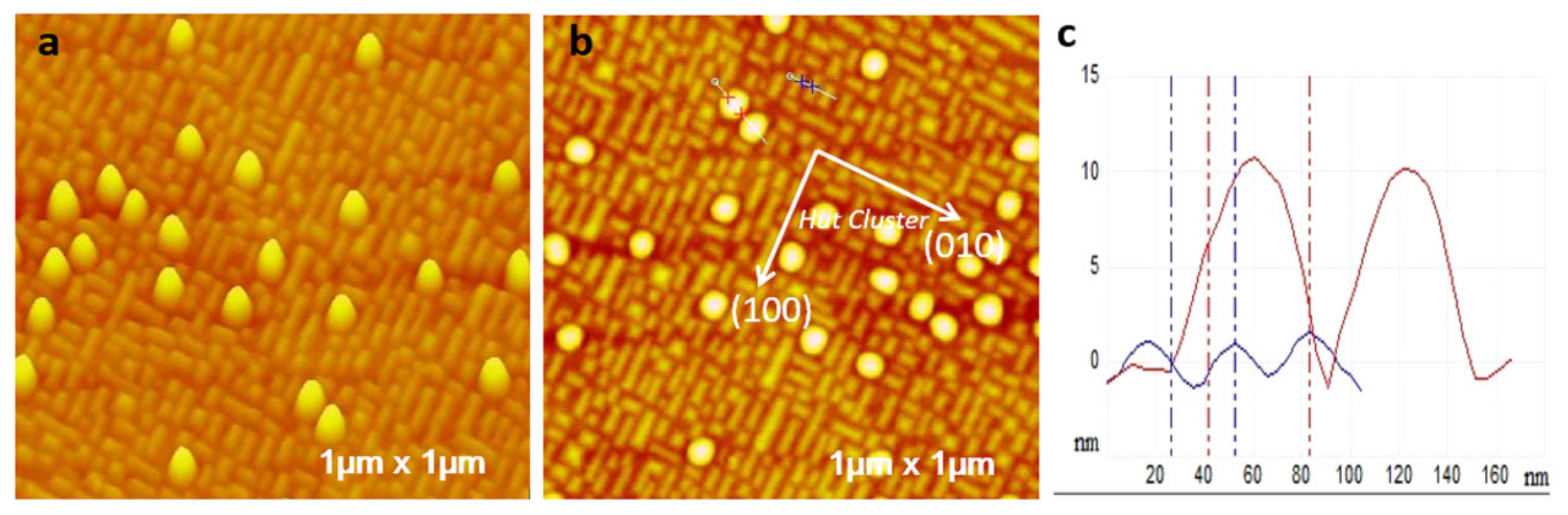
The structure of the corresponding QDs samples in
Figure 2 is slightly different from the above samples. Before the growth of Ge QDs, a 300 nm thick Si
0.8Ge
0.2 alloy layer was grown on the Si buffer layer. Subsequently, 8 ML Ge was deposited at 610 ℃. The introduction of the Si
0.8Ge
0.2 alloy layer before the growth of QDs strongly influenced the morphology. On the surface of the sample, two types of QDs formed: one was hut-shaped and the other was dome-shaped. The size and height of the dome-shaped QDs were similar to those of Ge QDs grown on Si substrates, with a diameter of about 50 nm and a height of about 10 nm. The newly emerged hut-shaped QDs were relatively special. The shape looked like a roof. The long sides were mainly distributed along the two crystal directions of (100) and (010). The width was about 20 nm, the length varied from 20 to 100 nm, and the height was about 2 nm. The formation of such hut-shaped QDs is related to the nucleation mechanism. Based on Stranski–Krastanow growth mode, initial Ge growth on SiGe virtual substrate occurred layer by layer. With further Ge deposition, islands formed due to large strain accumulation from the large lattice mismatch. A small three-dimensional island formed at the beginning was pyramid-shaped, that is, hut-shaped QDs. The large three-dimensional island formed later was domed, consisting of polycrystalline planes, which were dome-shaped QDs. Hut-shaped QDs form more easily and hence preferentially form first at higher density. They are metastable and act as an intermediate state of large dome-shaped QDs [
28]. The decreased surface mobility of Ge adatoms on the SiGe virtual layer promotes the nucleation of QDs, resulting in the growth of hut-shaped QDs with a high density.
Before the growth of Mn-doped Ge QDs, we needed to calibrate the doping concentration of Mn in Ge. The sample used for element calibration was a thin-film structure with a uniform composition based on the principle of measuring components by auger electron spectroscopy (AES). Therefore, we first used molecular beam epitaxy equipment to grow a 50 nm Si buffer layer on the Si substrate at 450 ℃ substrate temperature, and then an Mn-doped amorphous Ge film of about 10 nm was grown at room temperature to ensure that Mn was uniformly doped in the Ge film. A crystal oscillator controlled the growth rate of Si at 0.5 Å s−1, and the growth rate of Ge was 0.10 Å s−1. This was the same for the growth rates of MnGe QDs. Since the growth temperature was room temperature, Mn and Ge atoms were not likely to migrate on the substrate surface. Although the crystalline quality of the film was inferior and amorphous, the surface of the Mn-doped Ge film grown was flat and uniform in composition. Finally, the composition of Mn was determined to be 5% using AES measurement.
To better understand the effect of Mn doping on the growth of Ge QDs, we prepared multiple samples under similar conditions. The growth conditions are shown in
Table 1. T
S is the substrate temperature. There was no Mn element doping during the formation of QDs in Sample A. The substrate temperatures during the QDs growth were different between samples B and C. The Ge layer of sample B was grown at 610 ℃, whereas the growth temperature of the Ge layer of sample C varied from 500 to 610 ℃, where T
SS is the initial substrate temperature and T
SE is the substrate temperature at the end of growth.
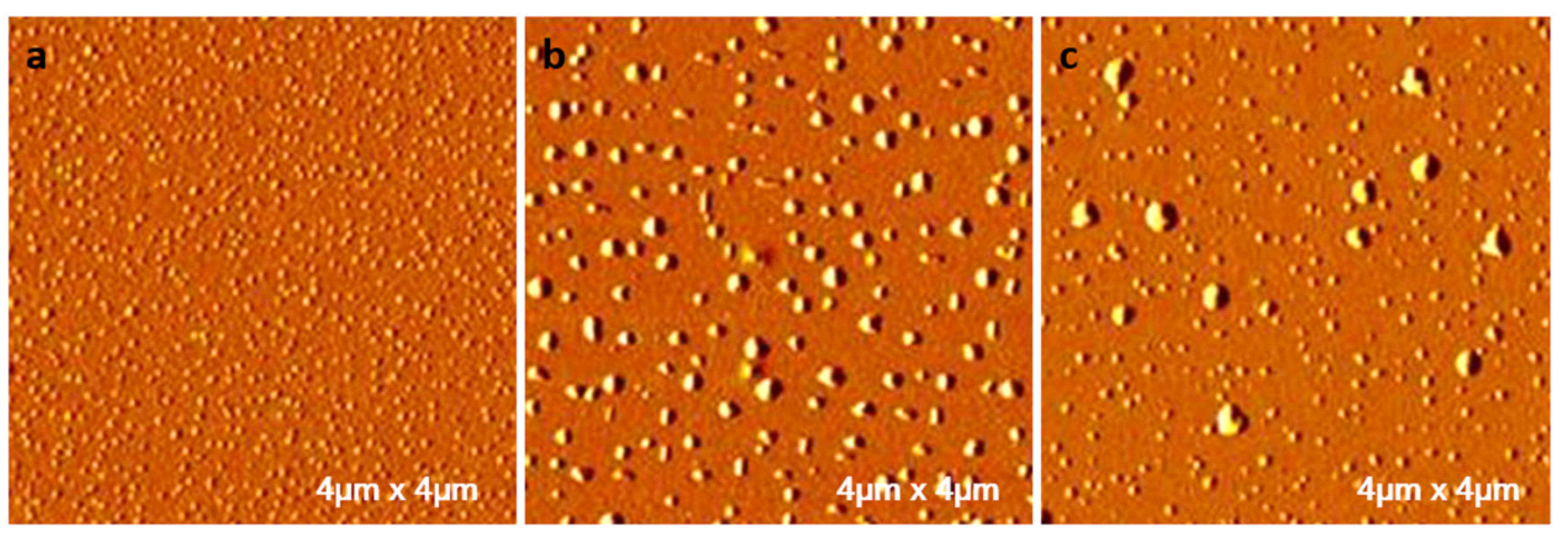
Figure 3a,b are the AFM morphology of samples A and B, respectively. Compared with the QDs sample without the doping of the Mn element as shown in
Figure 3a, after the introduction of Mn element doping (
Figure 3b), the QD size became varied, and the density dramatically reduced. There were sizeable dome-shaped QDs with diameters above 200 nm, small dome-shaped QDs with diameters between 50 and 150 nm, and individual rod-shaped structures. These morphological changes are directly related to the doping with the Mn. The introduction of Mn enhances the surface migration ability of the Ge, and the Ge atoms can find a more stable position at the same time, so the larger island-like QDs form. Simultaneously, the surface nanostructures are no longer perfect dome shapes, and even rod-shaped structures appear. The rod-shaped nanostructures can be attributed to the intermetallic compound phase [
18]. In our previous work, Mn
xGe
1−x QDs were grown on a SiGe virtual substrate, where Mn
5Ge
3 might form in small dome-shaped QDs [
24], and the presence of Mn
11Ge
8 was observed in the top Mn-rich region of the Si–SiGe/MnGe core-shell nanopillars, which we fabricated earlier [
25]. These results indicated that an intermetallic compound phase easily forms under improper growth conditions.
To further clarify the effect of substrate temperature on the growth process of Mn-doped QDs, a comparative analysis on samples B and C was conducted. Samples B and C were grown under conditions of fixed and variable temperature, respectively. As shown in
Figure 3b,c, the growth temperature had a significant effect on the morphology and growth process of Mn-doped Ge QD samples. QDs grown at variable temperature were obviously divided into two sizes, and the size distribution was relatively uniform. The size difference between the QDs grown at variable temperature was significant compared with QDs grown at fixed temperature. When the growth temperature was variable, some small QDs formed first, and these small QDs reunited together to form large QDs in the heating process. These results indicated that the growth of Mn-doped Ge QDs cannot be simply referred to as the growth process of Ge QDs, and the growth mechanism is unique. As a transition metal element, Mn has extremely low solid solubility in the Ge lattice, and it easily segregates the intermetallic phases from Ge lattice and destroys the original periodic lattice structure. In addition, the entry of Mn affects the surface mobility of Ge atoms, thus affecting the formation process of the QDs. Combined with the initial growth experience, we selected a suitable growth temperature zone and grew a series of Mn-doped Ge QDs samples.
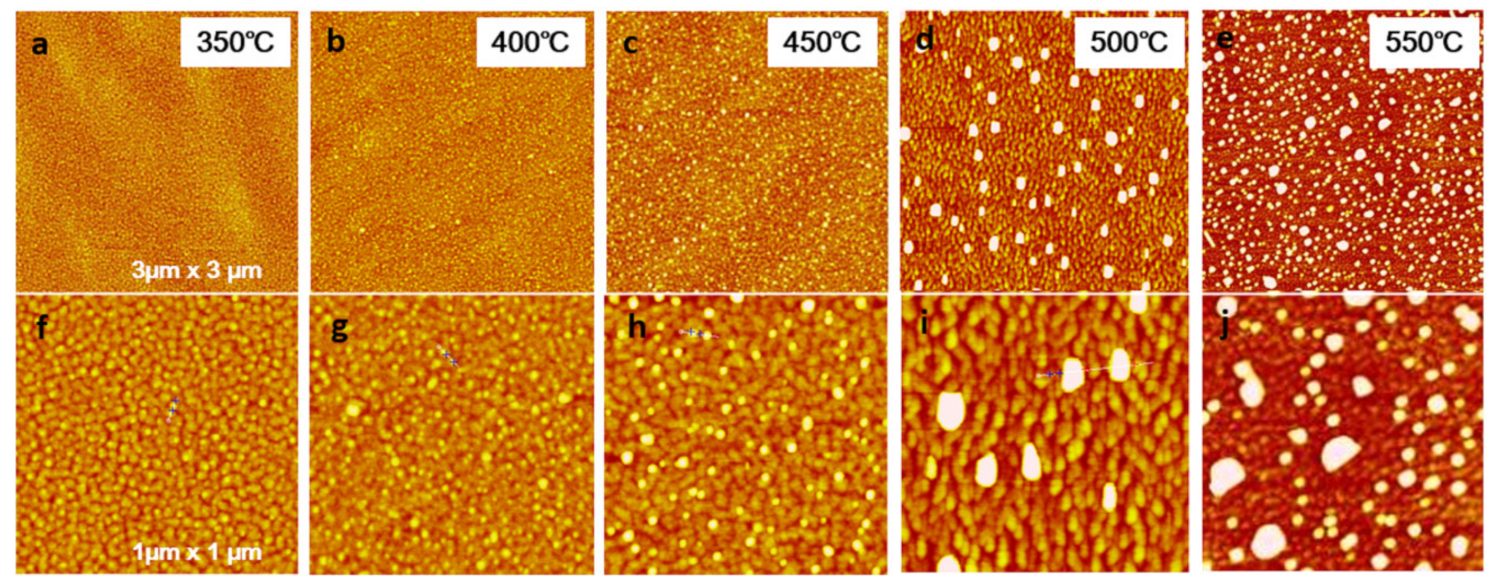
Figure 4 shows the surface morphology of Mn-doped Ge QD samples grown at different temperatures. The growth temperatures of the five samples were 350, 400, 450, 500, and 550 ℃. The Ge deposition thickness was 1.1 nm.
At a low growth temperature (350 ℃), there were exceptionally high-density dome-shaped QDs with uniform size, a diameter of about 25 nm, and a height of 2–3 nm. At a higher growth temperature (550 ℃), two sizes of dome-shaped QDs formed. The diameter of the large QDs was between 50 and 100 nm, and the height was close to 10 nm. However, the overall density was low and the shape of some large dome-shaped QDs was no longer standard. When the temperature was moderate (450 ℃), the surface of the sample is constructed with a layer of sparse QDs with a slightly larger size on the surface of the sample grown at low temperature(350 ℃). The sparse QDs have a diameter of about 40 nm, and a height of 4–5 nm. The shape of the dome was still relatively standard.
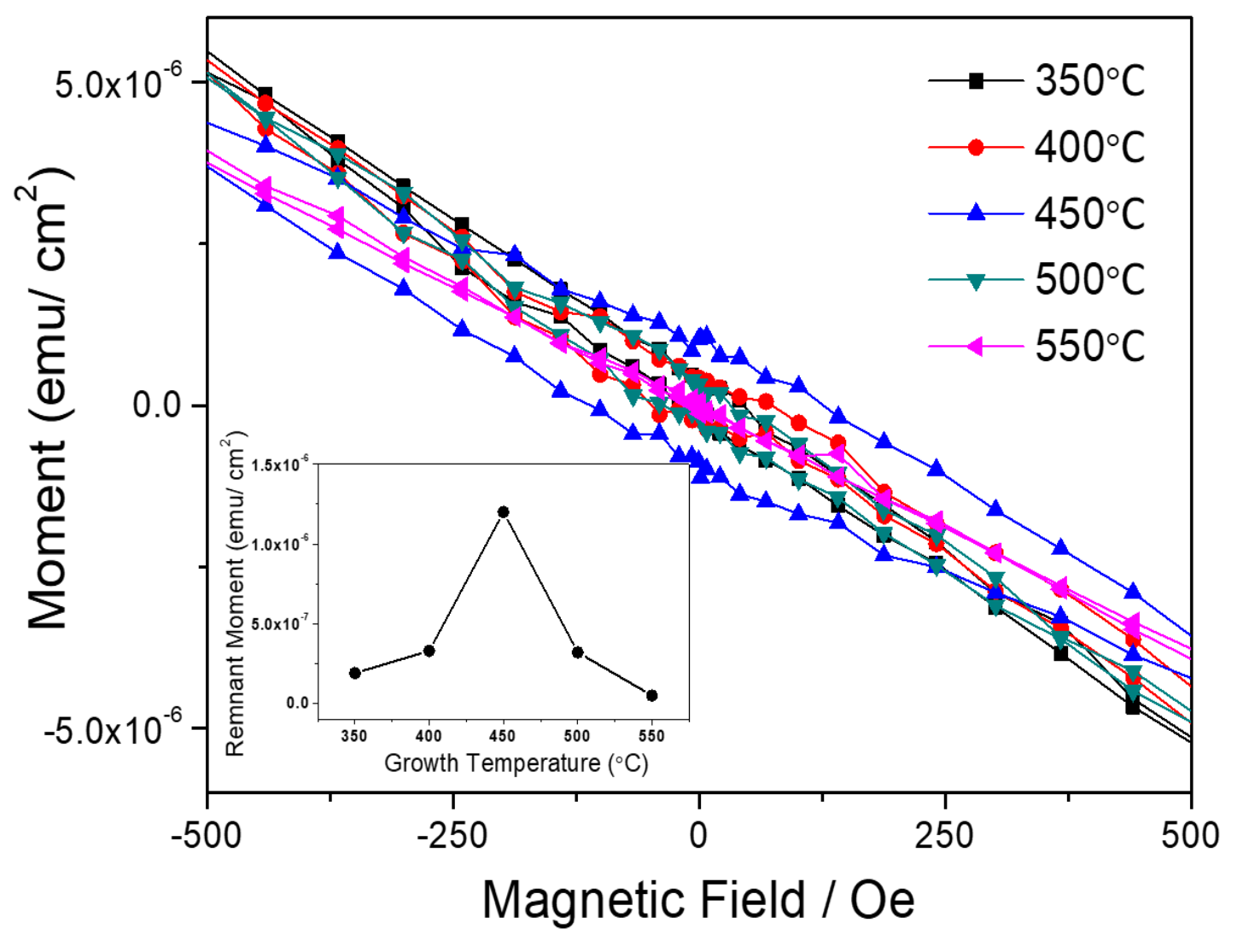
Figure 5 shows the hysteresis loops results of Mn-doped Ge QD samples at different growth temperatures. The growth temperatures of the five samples were 350, 400, 450, 500, and 550 ℃. Negative magnetic susceptibility occurred due to the diamagnetism of the Si substrate. Since the ferromagnetic signal was weak, the signal was not deducted to avoid errors caused by data processing. The inset is a comparison of the remanence of five samples. The Mn-doped Ge QD samples grown at 450 ℃ have visible hysteresis loop characteristics, which can be confirmed to have ferromagnetic characteristics. The QDs samples grown at 450 ℃ had the strongest ferromagnetism. Lowering or increasing the growth temperature led to the weakening of the ferromagnetism. When the growth temperature was reduced to 350 ℃ or increased to 550 ℃, the sample only showed the existence of diamagnetism.
The growth temperature had two effects on the Mn-doped Ge QD samples. (1) When the growth temperature was low, the quality of the crystal in the QD was poor, which was amorphous or polycrystalline. In our previous study of Si–SiGe/MnGe core-shell nanopillars, the uniform distribution of the Mn dopant and the amorphous state of the MnGe layer were observed by High Resolution Transmission Electron Microscope (HRTEM) images and Energy Dispersive Spectrometer (EDS) mappings in MnGe layer grown at a low temperature [
25]. Mn cannot reach the lattice substitution site in the lattice, and the energy band arrangement of the QD and the substrate is also distorted. The hole cannot be stabilized in the QD; thus, no effective indirect magnetic interaction between Mn ions can occur. (2) When the growth temperature is higher, the Mn has higher energy on the substrate, and it easily forms an intermetallic compound phase with Ge. The precipitation of the second phase greatly reduces the Mn effective doping and destroys the original periodic lattice structure. The intrinsic DMS ferromagnetic signal is weak. Generally, due to the strong ferromagnetism of many typical intermetallic compound phases, the intrinsic DMS ferromagnetic signal is likely to be buried.
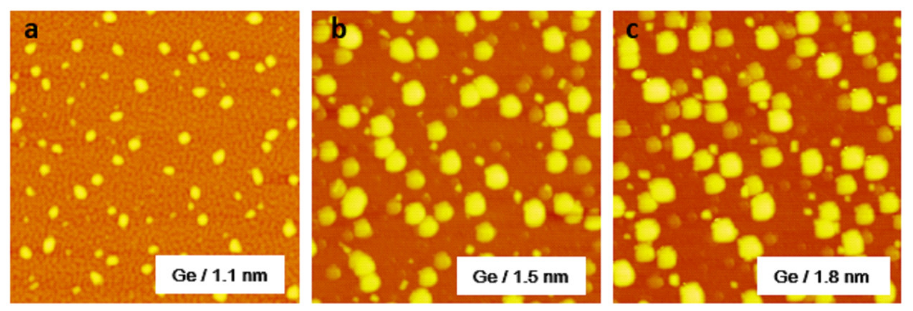
In addition, the effect of Ge deposition thickness on the morphology and magnetism of Mn-doped Ge QDs under the same concentration of Mn was studied. The growth of hetero-epitaxial Ge on a single-crystal Si lattice followed the growth pattern of Stranski–Krastanow. A certain thickness of Ge infiltration layer formed first. When Ge deposition exceeded a critical value, Ge grew into islands under the effect of stress release, and finally formed the QDs. Therefore, the amount of Ge deposition has a direct effect on the morphology and the magnetism of QDs.
Figure 6 shows the surface morphology of Mn-doped Ge QDs obtained under different thicknesses of Ge deposition. The QDs were grown on a 15 nm thick Si
0.8Ge
0.2 virtual substrate. In the samples corresponding to
Figure 6a–c, the deposition amounts of Ge are 1.1, 1.5, and 1.8 nm, respectively. We chose the deposition thickness using our long-term experience in growing Ge QDs. The deposition thickness of Ge has a more significant influence on the surface morphology of Mn-doped Ge QDs, and mainly on the size of QDs. As the deposition thickness increased, so did the size of the QDs, and a distinct hut-shaped structure appeared at 1.1 nm. More Ge migrated into the QDs, which increased the size of the QDs.
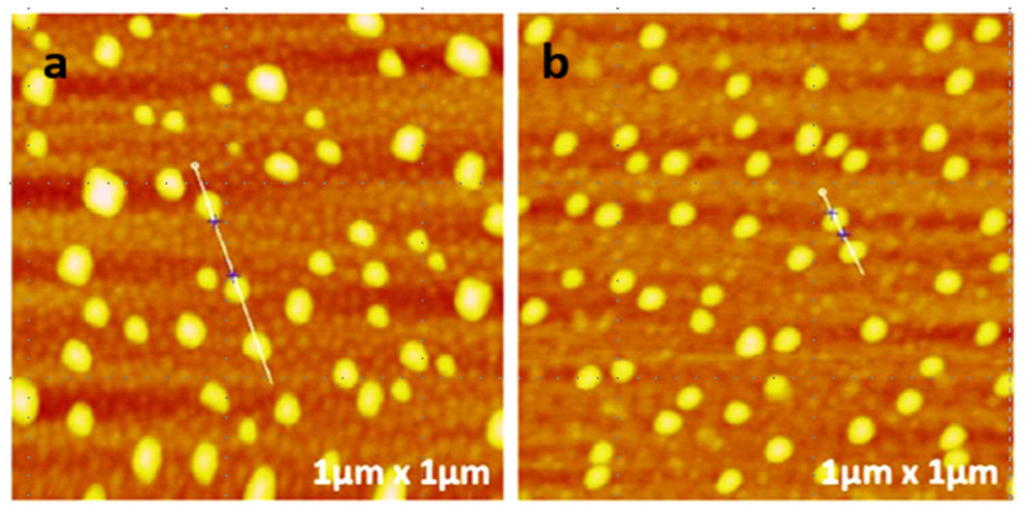
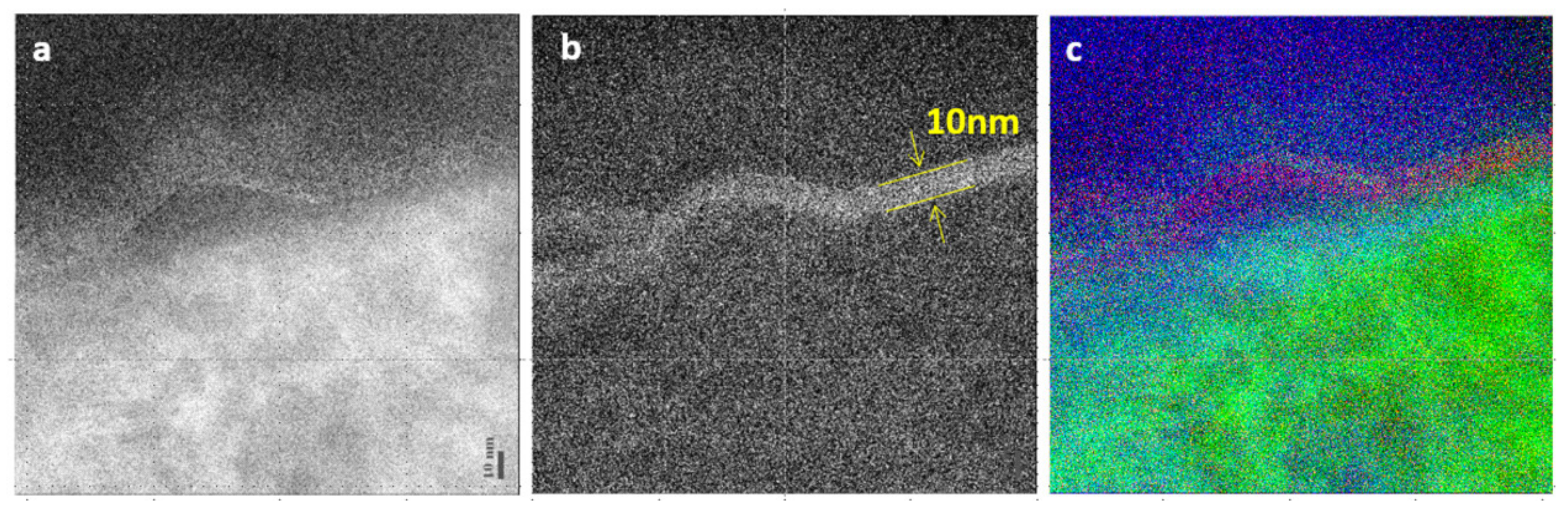
Figure 7 shows EFTEM maps of the MnGe QD sample grown on 15 nm thick Si
0.8Ge
0.2 virtual substrate (corresponding to
Figure 6a).
Figure 7a shows the distribution of Ge atoms in the substrate.
Figure 7b shows that the distribution profile of Mn atoms is a 10 nm thick strip on the sample surface.
Figure 7c is the false color map of EFTEM map. Green, blue, and red colors represent Si, Ge, and Mn atoms, respectively. This indicated that Mn dopants were uniformly distributed in the MnGe QD as well as the SiGe virtual thin layer.
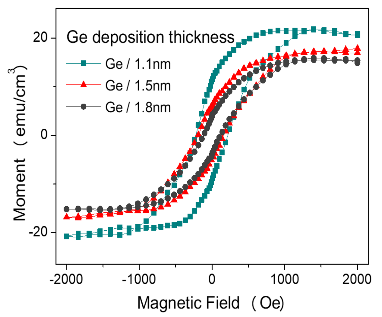
Figure 8 compares the hysteresis loops of Mn-doped Ge QD samples with different Ge deposits on the Si
0.8Ge
0.2 virtual substrate. The diamagnetism of the Si substrate was deducted. Its magnetic moment was converted into a magnetic moment per unit volume. The magnetic moment was saturated at high magnetic fields (H > 1.2 kOe). The weak negative susceptibility for Ge 1.1 nm and Ge 1.8 nm samples at high magnetic fields occurred due to errors from measurement and data processing. The samples with Ge deposition thickness of 1.1, 1.5, and 1.8 nm all showed distinct ferromagnetic characteristics at low temperature, and the samples with the deposition thickness of 1.1 nm had the largest saturation magnetic moment, remanence, and coercive force. When Ge deposition thickness increased to 1.5 and 1.8 nm, no hut-shaped dots were observed and the dome-shaped dots became larger (
Figure 6); both the saturation and the remnant moment simultaneously significantly reduced, as shown in
Figure 8. This means that the Mn atoms doped in the hut-shaped dots contributed more to ferromagnetism than those doped in the dome-shaped dots.


 ,
, 


