
Modern Trends in Microelectronics Packaging Reliability Testing

Abstract
:1. Introduction
2. Failure Rate, Time to Failure, and Acceleration Factor Modeling
3. Reliability Analysis and Life Prediction of Packaging Materials and Assemblies
3.1. Wire Bond Package Reliability Analysis
3.2. BGA Package Reliability
3.2.1. Thermal and Thermomechanical Stress Testing on Solder Joints
- (a)
- Pad matrix failure. In a study by Henshall et al., pad matrix failures are seen to occur across the matrix layer of the fiber–epoxy polymer composite of the PCB [25]. It is commonly observed as “cratering” on the side of the PCB.
- (b)
- Bulk solder failure: Bulk solder failure is the fracturing of the solder sphere. Darveaux et al. showed that this mode is more prone to occuring due to vibration failures [23]. The failure surface tends to be rougher than those seen for the UBM-IMC failures.
- (c)
- UBM–IMC failure: Failure cracks usually occur in intermetallic compounds (IMC), which are usually more brittle than bulk solder (Frear et al. 1999), or at the interface with the substrate [26]. They can be identified as a smooth surface on the die substrate or a characteristic ring step and smooth surface at the top of the solder bump.
3.2.2. High-Voltage and -Current-Stressed Solder Joint Studies
3.2.3. Impact and Vibration Stress Studies on Solder Joints
3.2.4. Life-Test Predictions of Solder Joint-Based Configurations
3.2.5. Device Failures in the Field
3.2.6. Failure Mechanism Coverage of Different Aging Tests
3.2.7. Aging and Prognostics Testing of Solder Joints
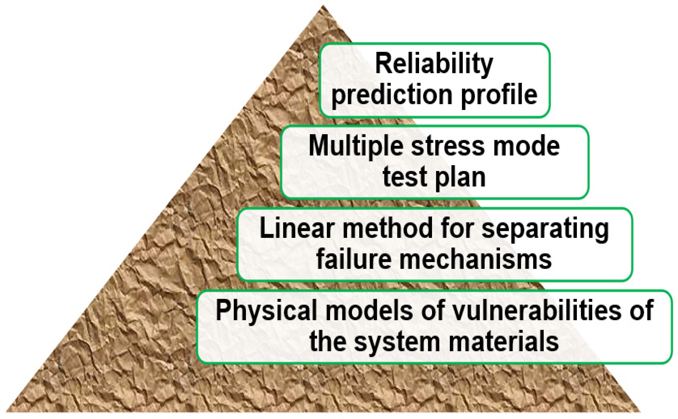
4. Methods for Separation of Failure Mechanisms in Packaging Assemblies
5. Latest Reliability Testing Studies on Advanced Package Assemblies
5.1. Outstanding Reliability Concerns in Advanced Packages

5.2. Reliability Analysis and Testing Performed on Advanced Packages
6. Conclusions
- (1)
- Failure mechanisms and testing methods of standard packaging schemes are considered acceptable qualification metrics for advanced packages based on most current studies.
- (2)
- Accurate reliability prediction in advanced packages will require testing methods more optimized than the standard methods used for conventional assemblies. The current testing standards propose product qualification based on accelerated tests in set stress conditions. The products pass the test if they endure the stress conditions after a given time.
- (3)
- Testing methods with single stress modes assume a single failure mechanism in the device. This assumption is observed to be inaccurate. Successful testing methods must succeed in revealing and separating multiple failure mechanisms.
- (4)
- Methods are in development for extraction and analysis of multiple data elements of standard and advanced packages. By deciphering the failure characteristics of the parts from the statistics of the results, accurate failure rates and failure times can be achieved. This will raise the bar for the reliability testing of advanced assemblies and complete systems.
Author Contributions
Funding
Institutional Review Board Statement
Informed Consent Statement
Data Availability Statement
Acknowledgments
Conflicts of Interest
References
- Qin, I.; Yauw, O.; Schulze, G.; Shah, A.; Chylak, B.; Wong, N. Advances in Wire Bonding Technology for 3D Die Stacking and Fan Out Wafer Level Package. In Proceedings of the 2017 IEEE 67th Electronic Components and Technology Conference (ECTC), Orlando, FL, USA, 30 May–2 June 2017; pp. 1309–1315. [Google Scholar]
- Howard, R. Packaging Reliability-How to Define and Measure It. IEEE Trans. Compon. Hybrids Manuf. Technol. 1982, 5, 454–462. [Google Scholar] [CrossRef]
- Lau, J. Chip on Board Technologies for Multichip Modules; Van Nostrand Reinhold: New York, NY, USA, 1994. [Google Scholar]
- Lau, J.; Pao, Y. Solder Joint Reliability of BGA, CSP, Flip Chip, and Fine Pitch SMT Assemblies; McGraw-Hill: New York, NY, USA, 1997. [Google Scholar]
- Lau, J.H. Semiconductor Advanced Packaging; Springer Publishers: Berlin/Heidelberg, Germany, 2021; ISBN 978-981-16-1375-3. [Google Scholar]
- Yoo, T. Advanced Chip Last Process Integration for Fan out WLP. In Proceedings of the 2022 IEEE 72nd Electronic Components and Technology Conference (ECTC), San Diego, CA, USA, 31 May–3 June 2022. [Google Scholar]
- Qin, C.; Li, Y.; Mao, H. Effect of Different PBO-Based RDL Structures on Chip-Package Interaction Reliability of Wafer Level Package. IEEE Trans. Device Mater. Reliab. 2020, 20, 524–529. [Google Scholar] [CrossRef]
- Wang, H.; Ma, J.; Yang, Y.; Gong, M.; Wang, Q. A Review of System-in-Package Technologies: Application and Reliability of Advanced Packaging. Micromachines 2023, 14, 1149. [Google Scholar] [CrossRef]
- Zhou, H.; Zhang, Y.; Cao, J.; Su, C.; Li, C.; Chang, A.; An, B. Research Progress on Bonding Wire for Microelectronic Packaging. Micromachines 2023, 14, 432. [Google Scholar] [CrossRef]
- Universal Approach for Using a Stress Sensing System for Package Development and Reliability Testing (T-9). Intelligent Reliability 4.0, Newsletter M36, vol. 5, 2023. Available online: https://www.irel40.eu/media (accessed on 28 February 2024).
- Bernstein, J.B.; Bensoussan, A.; Bender, E. Reliability Prediction for Microelectronics, 1st ed.; Wiley Series in Quality & Reliability Engineering; John Wiley & Sons: Hoboken, NJ, USA, 2024; ISBN 978-1394210930. [Google Scholar]
- McCluskey, F.; Hakim, E.; Fink, J.; Fowler, A.; Pecht, M. Reliability Assessment of Electronic Components Exposed to Long-Term Non-Operating Conditions. IEEE Trans. Compon. Packag. Manuf. Technol.-Part A 1998, 21, 352–359. [Google Scholar] [CrossRef]
- Boettge, B.; Naumann, F.; Behrendt, S.; Scheibel, M.; Kaessner, S.; Klengel, S.; Petzold, M.; Nickel, K.; Hejtmann, G.; Miric, A.-Z.; et al. Material Characterization of Advanced Cement-Based Encapsulation Systems for Efficient Power Electronics with Increased Power Density. In Proceedings of the IEEE 68th Electronic Components and Technology Conference, San Diego, CA, USA, 29 May–1 June 2018; pp. 1258–1269. [Google Scholar]
- Uebbing, J. Mechanisms of Temperature Cycle Failure in Encapsulated Optoelectronic Devices. In Proceedings of the 19th International Reliability Physics Symposium, (IRPS), Las Vegas, NV, USA, 7–9 April 1981; pp. 149–156. [Google Scholar]
- Hund, T.; Plunkett, P. Improving Thermosonic Gold Ball Bond Reliability. IEEE Trans. Compon. Hybrids Manuf. Technol. 1985, 8, 446–456. [Google Scholar] [CrossRef]
- Khan, M.; Fatemi, H.; Romero, J.; Delenia, E. Effect of High Thermal Stability Mold Material on the Gold-Aluminum Bond Reliability in Epoxy Encapsulated VLSI Devices. In Proceedings of the International Reliability Physics Symposium (IRPS), Anaheim, CA, USA, 30 March–2 April 1998; pp. 40–49. [Google Scholar]
- Park, J.; Kim, B.S.; Cha, H.J.; Jo, Y.B.; Shin, S.C.; Kim, G.R.; Park, J.K.; Shin, M.Y.; Ouh, K.I.; Jeon, H.G. Interfacial Degradation Mechanism of Au-Al Bonding in Quad Flat Package. In Proceedings of the IEEE 42nd Annual International Reliability Physics Symposium, Phoenix, AZ, USA, 25–30 April 2004; pp. 569–570. [Google Scholar]
- Zhang, L.; Hunter, B.; Subbarayan, G.; Rose, D. The Accuracy of Structural Approximations Employed in Analysis of Area Array Packages. IEEE Trans. Compon. Packag. Technol. 1999, 22, 525–533. [Google Scholar] [CrossRef]
- Bhate, D.; Chan, D.; Subbarayan, G.; Chiu, T.; Gupta, V.; Edwards, D. Constitutive Behavior of Sn3.8Ag0.7Cu and Sn1.0Ag0.5Cu Alloys at Creep and Low Strain Rate Regimes. IEEE Trans. Compon. Packag. Technol. 2008, 31, 622–633. [Google Scholar] [CrossRef]
- Kumar, P.; Huang, Z.; Chavali, S.; Chan, D.; Dutta, I.; Subbarayan, G.; Gupta, V. Microstructurally Adaptive Model for Primary and Secondary Creep of Sn-Ag-Based Solders. IEEE Trans. Compon. Packag. Technol. 2012, 2, 256–265. [Google Scholar] [CrossRef]
- Mysore, K.; Subbarayan, G.; Gupta, V.; Zhang, R. Constitutive and Aging Behavior of Sn3.0Ag0.5Cu Solder Alloy. IEEE Trans. Compon. Packag. Technol. 2009, 32, 221–232. [Google Scholar] [CrossRef]
- Nee, A. Handbook of Manufacturing Engineering and Technology; Springer: Berlin/Heidelberg, Germany, 2015; ISBN 978-1-4471-4669-8. [Google Scholar]
- Darveaux, R.; Reichman, C.; Islam, N. Interface failure in lead free solder joints. In Proceedings of the 56th Electronic Components and Technology Conference ECTC, San Diego, CA, USA, 30 May–2 June 2006; p. 12. [Google Scholar]
- Zhao, X.; Caers, J.; de Vries, J.; Wong, E.; Rajoo, R. A component level test method for evaluating the resistance of Pb-free BGA solder joints to brittle fracture under shock impact. In Proceedings of the 57th Proceedings of Electronic Components and Technology Conference ECTC, Sparks, NV, USA, 29 May–1 June 2007; p. 1522. [Google Scholar]
- Henshall, G.; Healey, R.; Pandher, R.; Sweatman, K.; Howell, K.; Coyle, R.; Sack, T.; Snugovsky, P.; Tisdale, S.; Hua, F. iNEMI Pb-free alloy alternatives project report: State of the industry. In Proceedings of the Surface Mount Technology Association Conference, Orlando, FL, USA, 17–21 August 2008. [Google Scholar]
- Frear, D.; Morgan, H.; Burchett, S.; Lau, J. The Mechanics of Solder Alloy Interconnects; Chapman & Hall: New York, NY, USA, 1999. [Google Scholar]
- Ouyang, F.; Tu, K.N.; Lai, Y. Effect of electromigration induced joule heating and strain on microstructural recrystallization in eutectic SnPb flip chip solder joints. Mater. Chem. Phys. 2012, 136, 210–218. [Google Scholar] [CrossRef]
- Dandu, P.; Fan, X.J.; Liu, Y.; Diao, C. Finite element modeling on electromigration of solder joints in wafer level packages. Microelectron. Reliab. 2010, 50, 547–555. [Google Scholar] [CrossRef]
- Dandu, P.; Fan, X.J. Assessment of Current Density Singularity in Electromigration of Solder Bumps. In Proceedings of the 2011 IEEE 61st Electronic Components and Technology Conference (ECTC), Lake Buena Vista, FL, USA, 31 May–3 June 2011. [Google Scholar]
- Alam, M.O.; Wu, B.Y.; Chan, Y.C.; Tu, K.N. High electric current density-induced interfacial reactions in micro ball grid array (µBGA) solder joints. Acta Mater. 2006, 54, 613–621. [Google Scholar] [CrossRef]
- Gan, H.; Choi, W.J.; Xu, G.; Tu, K.N. Electromigration in Solder Joints and Solder Lines. JOM 2002, 54, 34–37. [Google Scholar] [CrossRef]
- Fan, X.; Ranouta, A. Finite Element Modeling of System Design and Testing Conditions for Component Solder Ball Reliability Under Impact. IEEE Trans. Compon. Packag. Manuf. Technol. 2012, 2, 1802–1810. [Google Scholar] [CrossRef]
- Lou, H.; Qu, X.; Chen, Z.; Wang, J.; Lee, T.; Wang, H. Lifetime Assessment of Solder Joints of BGA Package in Board Level Drop Test. In Proceedings of the IEEE 6th International Conference on Electronic Packaging Technology, Shenzhen, China, 30 August–2 September 2005. [Google Scholar]
- Asasaari, S.; Fadil, N.; Tamin, M. Mechanics of solder/IMC interface of lead-free solder interconnects in ball grid array assembly. J. Mech. Eng. Sci. 2021, 16, 8718–8729. [Google Scholar] [CrossRef]
- Meade, D. Failure Rate Estimation in the Case of Zero Failures. In Microelectronic Manufacturing Yield, Reliability, and Failure Analysis III.; SPIE: Bellingham, WA, USA, 1997; Volume 3216. [Google Scholar]
- Relex Software Corporation. Calculating MTTF When You Have Zero Failures. Technical Brief. 1993. Available online: https://www.relexsolutions.com/ (accessed on 28 February 2024).
- Bernstein, J.; Gurfinkel, M.; Li, X.; Walters, J.; Shapira, Y.; Talmor, M. Electronic circuit reliability modeling. Microelectron. Reliab. 2006, 46, 1957–1979. [Google Scholar] [CrossRef]
- JESD22-A110E.01; Highly Accelerated Temperature and Humidity Stress Test (HAST). JEDEC: Arlington, VA, USA, 2012.
- Merrett, R.; Bryant, J.; Studd, R. An Appraisal of High Temperature Humidity Stress Tests for Assessing Plastic Encapsulated Semiconductor Components. In Proceedings of the 21st International Reliability Physics Symposium, (IRPS), Phoenix, AZ, USA, 5–7 April 1983; pp. 73–82. [Google Scholar]
- Shirley, C.; Blish, R. Thin-Film Cracking and Wire Ball Shear in Plastic Dips Due to Temperature Cycle and Thermal Shock. In Proceedings of the 25th International Reliability Physics Symposium, San Diego, CA, USA, 7–9 April 1987; pp. 238–249. [Google Scholar]
- Blish, R.; Vaney, P. Failure Rate Model for Thin Film Cracking in Plastic ICs. In Proceedings of the 29th Annual Proceedings International Reliability Physics Symposium (IRPS), Las Vegas, NV, USA, 9–11 April 1991; pp. 22–29. [Google Scholar]
- Hu, K.X.; Yeh, C.-P.; Doot, B.; Skipor, A.; Wyatt, K. Die Cracking in Flip-Chip-on-Board Assembly. In Proceedings of the 45th Electronic Components and Technology Conference, Las Vegas, NV, USA, 21–24 May 1995; pp. 293–299. [Google Scholar]
- Annaniah, L.; Devarajan, M.; San, T.K. An Investigation on Die Crack Detection Using Temperature Sensitive Parameter for High Speed LED Mass Production. Results Phys. 2017, 7, 3882–3891. [Google Scholar] [CrossRef]
- Emerson, J.; Sweet, J.; Peterson, D. Evaluating Plastic Assembly Processes for High Reliability Applications Using HAST and Assembly Test Chips. In Proceedings of the International Reliability Physics Symposium (IRPS), San Jose, CA, USA, 11–14 April 1994; pp. 191–195. [Google Scholar]
- Tanaka, N.; Kitano, M.; Kumazawa, T.; Nishimura, A. Evaluating IC-package Interface Delamination by Considering Moisture-Induced Molding-Compound Swelling. IEEE Trans. Compon. Packag. Technol. 1999, 22, 426–432. [Google Scholar] [CrossRef]
- Aihara, T.; Ito, S.; Sasajima, H.; Oota, K. Development of Reliability and Moldability on Fine Pitch Ball Grid Array by Optimizing Materials. J. Electron. Packag. 2001, 123, 88. [Google Scholar] [CrossRef]
- Chung, C.; Fun, J.; Huang, M.; Tsai, F. Study on Failure Mechanism of PCT Reliability for BT Substrate Based CSP (Chip Scale Packages). Trans. Am. Soc. Mech. Eng. (ASME) 2002, 124, 334–339. [Google Scholar] [CrossRef]
- Saitoh, T.; Matsuyama, H.; Toya, M. Delamination and Encapsulant Resin Cracking in LSI Plastic Packages Subjected to Temperature Cyclic Loading. J. Electron. Packag. 2003, 125, 420–425. [Google Scholar] [CrossRef]
- Kwon, W.-S.; Yim, M.-J.; Paik, K.-W.; Ham, S.-J.; Lee, S.-B. Thermal Cycling Reliability and Delamination of Anisotropic Conductive Adhesives Flip Chip on Organic Substrates with Emphasis on the Thermal Deformation. J. Electron. Packag. 2005, 127, 86–90. [Google Scholar] [CrossRef]
- Braun, T.; Becker, K.; Koch, M.; Bader, V.; Aschenbrenner, R.; Reichl, H. High-Temperature Reliability of Flip Chip Assemblies. Microelectron. Reliab. 2006, 46, 144–154. [Google Scholar] [CrossRef]
- Liu, H.; Pang, X.; Xu, S. Failure Mechanism Study for Low-k Device Bond Pad Crack Post Temperature Cycle. In Proceedings of the 21st Electronics Packaging Technology Conference (EPTC), Singapore, 4–6 December 2019; pp. 208–212. [Google Scholar]
- Kho, K.; You, G.; Tan, G.; Hsu, C.-T.; Guan, H. Detecting Wire Bond Inter Layer Dielectric Crack by Dark Field Imaging. In Proceedings of the IEEE 23rd Electronics Packaging Technology Conference (EPTC), Singapore, 1–3 December 2021; pp. 104–107. [Google Scholar]
- Zelenka, R. A reliability model for interlayer dielectric cracking during temperature cycling. In Proceedings of the 29th Annual Proceedings International Reliability Physics Symposium (IRPS), Las Vegas, NV, USA, 9–11 April 1991. [Google Scholar]
- Amagai, M.; Seno, H.; Ebe, K. Cracking Failures in Lead-on-Chip Packages Induced by Chip Backside Contamination. IEEE Trans. Compon. Packag. Manuf. Technol.-Part B 1995, 18, 119–126. [Google Scholar] [CrossRef]
- Dias, R.; Lucero, A.; Niemeyer, S.; Myers, S. Failure Mechanisms in C4 Organic Packages. In Proceedings of the Intel Q&R Conference, Santa Clara, CA, USA, 15 September 1997; pp. 57–68. [Google Scholar]
- Ahn, E.C.; Cho, T.J.; Shin, J.B.; Moon, H.J.; Lyu, J.H.; Choi, K.W.; Kang, S.Y.; Oh, S.Y. Reliability of Flip Chip BGA Package on Organic Substrate. In Proceedings of the 50th Electronic Components and Technology Conference (Cat. No.00CH37070), Las Vegas, NV, USA, 21–24 May 2000; pp. 1215–1220. [Google Scholar]
- Lin, Y.; Liu, W.; Guo, Y.; Shi, F. Reliability Issues of Low-Cost Overmolded Flip Chip Packages. IEEE Trans. Adv. Packag. 2005, 28, 79–88. [Google Scholar]
- Mercado, L.; Wieser, H.; Hauck, T. Multichip Package Delamination and Die Fracture Analysis. IEEE Trans. Adv. Packag. 2003, 26, 152–159. [Google Scholar] [CrossRef]
- Tu, P.; Chan, Y.; Lai, J. Effect of Intermetallic Compounds on the Thermal Fatigue of Surface Mount Solder Joints. IEEE Trans. Compon. Packag. Manuf. Technol. -Part B 1997, 20, 87–93. [Google Scholar] [CrossRef]
- Suhling, J.C.; Gale, H.S.; Johnson, R.W.; Islam, M.N.; Shete, T.; Lall, P.; Bozack, M.J.; Evans, J.L.; Seto, P.; Gupta, T.; et al. Thermal Cycling Reliability of Lead-Free Solders for Automotive Applications. In Proceedings of the 9th Intersociety Conference on Thermal and Thermomechanical Phenomena in Electronic Systems, Las Vegas, NV, USA, 1–4 June 2004; pp. 350–357. [Google Scholar]
- Wang, G.; Groothuis, S.; Ho, P. Packaging Effect on Reliability for Cu/Low-k Structure. In Proceedings of the IEEE 42nd Annual International Reliability Physics Symposium, Phoenix, AZ, USA, 25–30 April 2004; pp. 557–562. [Google Scholar]
- Birzer, C.; Stoeckl, S.; Schuetz, G.; Fink, M. Reliability Investigations of Leadless QFN Packages until End-of-life with Application-Specific Board-Level Stress Tests. In Proceedings of the IEEE ECTC 56th Electronic Components and Technology Conference, San Diego, CA, USA, 30 May–2 June 2006; pp. 594–600. [Google Scholar]
- Davis, J.; Bozack, M.; Evans, J. Effect of (Au, Ni)Sn4 Evolution on Sn-37Pb/ENIG Solder Joint Reliability Under Isothermal and Temperature-Cycled Conditions. IEEE Trans. Compon. Packag. Technol. 2007, 30, 32–41. [Google Scholar] [CrossRef]
- Ghaffarian, R. Reliability of Package on Package (PoP) Assembly Under Thermal Cycles. In Proceedings of the IEEE Intersociety Conference on Thermal and Thermomechanical Phenomena in Electronic Systems (ITherm), Las Vegas, NV, USA, 28–31 May 2019; pp. 472–476. [Google Scholar]
- Wu, W.; Held, M.; Jacob, P.; Scacco, P.; Birolini, A. Thermal stress related packaging failure in power IGBT modules. In Proceedings of the International Symposium on Power Semiconductor Devices and IC’s: ISPSD ′95, Yokohama, Japan, 23–25 May 1995; pp. 330–334. [Google Scholar]
- Cory, A. Improved Reliability Prediction Through Reduced—Stress Temperature Cycling. In Proceedings of the IEEE 38th Annual International Reliability Physics Symposium, San Jose, CA, USA, 10–13 April 2000; pp. 231–236. [Google Scholar]
- Tang, W.; Long, X.; Yang, F. Tensile Deformation and Mirostructures of Sn–3.0Ag–0.5Cu Solder Joints: Effect of Annealing Temperature. Microelectron. Reliab. 2020, 104, 113555. [Google Scholar] [CrossRef]
- Xu, J.; Guo, Y.; Su, Y.; Tang, R.; Long, X. Growth Kinetics of Intermetallic Compound in Solder Joints During Thermal Cycling: A Review. In Proceedings of the IEEE 23rd Electronics Packaging Technology Conference (EPTC), Singapore, 1–3 December 2021; pp. 464–468. [Google Scholar]
- Striny, K.; Schelling, A. Reliability Evaluation of Aluminum-Metallized MOS Dynamic RAM’s in Plastic Packages in High Humidity and Temperature Environments. IEEE Trans. Compon. Hybrids Manuf. Technol. 1981, 4, 476–481. [Google Scholar] [CrossRef]
- Emerson, J.; Peterson, D.; Sweet, J. HAST Evaluation of Organic Liquid IC Encapsulant Using Sandia’s Assembly Test Chips. In Proceedings of the International Reliability Physics Symposium (IRPS), San Diego, CA, USA, 18–20 May 1992; pp. 951–956. [Google Scholar]
- Pecht, M.; Dasgupta, A. Physics of Failure: An Approach to Reliable Product Development. In Proceedings of the IEEE 1995 International Integrated Reliability Workshop, Final Report, Lake Tahoe, CA, USA, 22–25 October 1995; pp. 1–4. [Google Scholar]
- Tran, T.; Yong, L.; Williams, B.; Chen, S.; Chen, A. Fine Pitch Probing and Wirebonding and Reliability of Aluminum Capped Copper Bond Pads. In Proceedings of the 50th Electronic Components and Technology Conference (Cat. No.00CH37070), Las Vegas, NV, USA, 21–24 May 2000; pp. 1674–1680. [Google Scholar]
- Wagner, S.; Hoeppner, K.; Toepper, M.; Wittler, O.; Lang, K. A Critical Review of Corrosion Phenomena in Microelectronic Systems. In Proceedings of the PCIM Europe, International Conference for Power Electronics, Intelligent Motion, Renewable Energy and Energy Management, Nuremberg, Germany, 20–22 May 2014; pp. 1–7. [Google Scholar]
- Wu, J.; Lee, C.; Zheng, P.; Lee, J. Electromigration Reliability of SnAgxCuy Flip Chip Interconnects. In Proceedings of the 54th Electronic Components and Technology Conference (IEEE Cat. No.04CH37546), Las Vegas, NV, USA, 4 June 2004; pp. 961–967. [Google Scholar]
- Balkan, H. Flip Chip Electromigration: Impact of Test Conditions in Product Life Predictions. In Proceedings of the 54th Electronic Components and Technology Conference (IEEE Cat. No.04CH37546), Las Vegas, NV, USA, 4 June 2004; pp. 983–987. [Google Scholar]
- Shao, T.; Chen, I.H.; Chen, C. Electromigration Failure Mechanism of Sn96.5Ag3.5 Flip Chip Solder Bumps. In Proceedings of the 54th Electronic Components and Technology Conference (IEEE Cat. No.04CH37546), Las Vegas, NV, USA, 4 June 2004; pp. 979–982. [Google Scholar]
- Basaran, C.; Ye, H.; Hopkins, D.; Frear, D.; Lin, J. Failure Modes of Flip Chip Solder Joints Under High Electric Current Density. Trans. ASME J. Electron. Packag. 2005, 127, 157–163. [Google Scholar] [CrossRef]
- Ding, M.; Wang, G.; Chao, B.; Ho, P.; Su, P.; Uehling, T.; Wontor, D. A Study of Electromigration Failure in Pb-free Solder Joints. In Proceedings of the 43th International Reliability Physics Symposium (IRPS), San Jose, CA, USA, 17–21 April 2005; pp. 518–523. [Google Scholar]
- Tajedini, M.; Osmanson, A.T.; Kim, Y.R.; Madanipour, H.; Kim, C.U.; Glasscock, B.; Khan, M. Electromigration Effect on the Pd Coated Cu Wirebond. In Proceedings of the IEEE 71st Electronic Components and Technology Conference (ECTC), San Diego, CA, USA, 1–4 June 2021. [Google Scholar]
- Lin, Y.; Peng, C.; Chiang, K. Parametric Design and Reliability Analysis of Wire Interconnect Technology Wafer Level Packaging. ASME J. Electron. Packag. 2002, 124, 234–239. [Google Scholar] [CrossRef]
- Liu, X.; Sooklal, V.; Verges, M.; Larson, M. Experimental Study and Life Prediction on High Cycle Vibration Fatigue in BGA Packages. Microelectron. Reliab. 2006, 46, 1128–1138. [Google Scholar] [CrossRef]
- Noctor, D.; Bader, F.; Viera, A.; Boysan, P.; Golwalkar, S.; Foehringer, R. Attachment Reliability Evaluation and Failure Analysis of Thin Small Outline Packages (TSOP’s) with Alloy 42 Lead Frames. IEEE Trans. Compon. Hybrids Manuf. Technol. 1993, 16, 961–971. [Google Scholar] [CrossRef]
- Jeon, Y.; Lee, Y.; Choi, Y. Thin Electroless Cu/OSP on Electroless Ni as a Novel Surface Finish for Flip Chip Solder Joints. In Proceedings of the IEEE 56th Electronic Components and Technology Conference (ECTC), San Diego, CA, USA, 30 May–2 June 2006; pp. 119–124. [Google Scholar]
- Amagai, M. The Effect of Polymer Die Attach Material on Solder Joint Reliability. In Proceedings of the Workshop on Mechanical Reliability of Polymer Materials and Plastic Packages of IC Devices, Paris, France, 29 November–2 December 1998; Volume 25, pp. 223–230. [Google Scholar]
- Scalise, J. Plastic Encapsulated Microcircuits (PEM) Qualification Testing. In Proceedings of the 1996 IEEE ECTC, Orlando, FL, USA, 28–31 May 1996; pp. 392–397. [Google Scholar]
- Danielson, D.; Marcyk, G.; Babb, E.; Kudva, S. HAST Applications: Acceleration Factors and Results for VLSI Components. In Proceedings of the 1989 IEEE/IRPS, Phoenix, AZ, USA, 11–13 April 1989; pp. 114–121. [Google Scholar]
- Gershman, I.; Bernstein, J. Nondestructive Quantitative Analysis of Crack Propagation in Solder Joints. IEEE Trans. Compon. Packag. Manuf. Technol. 2013, 3, 1263–1270. [Google Scholar] [CrossRef]
- Gershman, I.; Bernstein, J. Solder-Joint Quantitative Crack Analysis—Ohmic Resistance Approach. IEEE Trans. Compon. Packag. Manuf. Technol. 2012, 2, 748–755. [Google Scholar] [CrossRef]
- Gershman, I.; Bernstein, J. Structural health monitoring of solder joints in QFN package. Microelectron. Reliab. 2012, 52, 3011–3016. [Google Scholar] [CrossRef]
- Hofmeister, J.; Lall, P.; Panchagade, D.; Roth, N.; Tracy, T.; Judkins, J.; Harris, K. Ball Grid Array (BGA) Solder Joint Intermittency Detection: SJ BIST™. In Proceedings of the IEEE Aerospace Conference, Big Sky, MT, USA, 1–8 March 2008. [Google Scholar]
- Kanie, H.; Nonaka, Y. Estimation of Weibull shape-parameters for two independent competing risks. IEEE Trans. Rel. 1985, 34, 53–56. [Google Scholar] [CrossRef]
- Hsu, S.-H.; Yang, K.; Milor, L. Machine learning for detection of competing wearout mechanisms. In Proceedings of the IEEE International Reliability Physics Symposium (IRPS), Monterey, CA, USA, 31 March–4 April 2019; pp. 1–9. [Google Scholar]
- Chakraborty, U.; Bender, E.; Boning, D.S.; Thompson, C.V. Identification of Multiple Failure Mechanisms for Device Reliability Using Differential Evolution. IEEE Trans. Device Mater. Reliab. 2023, 23, 599–614. [Google Scholar] [CrossRef]
- Chery, E.; Fohn, C.; Messemaeker, J.; Beyne, E. Reliability Challenges in Advanced 3D Technologies: The Case of through Silicon Vias and SiCN–SiCN Wafer-to-Wafer Hybrid-Bonding Technologies. IEEE Trans. Device Mater. Reliab. 2023, 23, 615–622. [Google Scholar] [CrossRef]
- Yip, L.; Tsai, J.; Lin, R.; Hsu, I. 2.5D MCM (Multi-chip Module) Technology Development for Advanced Package. In Proceedings of the 2023 IEEE 73rd Electronic Components and Technology Conference (ECTC), Orlando, FL, USA, 30 May–2 June 2023; pp. 778–782. [Google Scholar] [CrossRef]
- Murai, K.; Onozeki, H.; Kang, D.; Hirano, K.; Mitsukura, K. Study of Fabrication and Reliability for the Extremely Large 2.5D Advanced Package. In Proceedings of the 2023 IEEE 73rd Electronic Components and Technology Conference (ECTC), Orlando, FL, USA, 30 May–2 June 2023; pp. 899–906. [Google Scholar] [CrossRef]
- Lee, S.; Chen, K.; Lu, J. Wafer-to-Wafer Alignment for Three-Dimensional Integration: A Review. IEEE J. Microelectromechanical Syst. 2011, 20, 885–898. [Google Scholar] [CrossRef]
- La Tulipe, D.; Shi, L.; Topol, A.; Frank, D.; Steen, S.; Pfeiffer, D.; Posillico, D.; Neumayer, D.; Goma, S.; Vichiconti, J.; et al. Critical aspects of layer transfer and alignment tolerances for 3D integration processes. In Proceedings of the 3D Packaging Workshop IMAPS Device Packaging Conference, Scottsdale, AZ, USA, 19–21 March 2006. Paper THP22. [Google Scholar]
- Chen, K.-N.; Lee, S.H.; Andry, P.S.; Tsang, C.K.; Topol, A.W.; Lin, Y.-M.; Lu, J.-Q.; Young, A.M.; Ieong, M.; Haensch, W. Structure design and process control for Cu bonded interconnects in 3D integrated circuits. In Proceedings of the 2006 International Electron Devices Meeting, San Francisco, CA, USA, 11–13 December 2006; pp. 20–22. [Google Scholar]
- Kim, H.; Najafi, K. Characterization of low-temperature wafer bonding using thin-film parylene. J. Microelectromech. Syst. 2005, 14, 1347–1355. [Google Scholar] [CrossRef]
- Lee, M.C.; Kang, S.J.; Jung, K.D.; Cho, S.-H.; Cho, Y.C. A high yield rate MEMS gyroscope with a packaged SiOG process. J. Micromech. Microeng. 2005, 15, 2003–2010. [Google Scholar] [CrossRef]
- Iyer, S.; Bajwa, A. Reliability Challenges in Advance Packaging. In Proceedings of the 2018 IEEE International Reliability Physics Symposium, Burlingame, CA, USA, 11–15 March 2018; pp. 4D.5-1–4D.5-4. [Google Scholar] [CrossRef]
- Liu, C.; Chen, J.; Hsu, Y.; Wang, R.; Wang, Y.; Ho, B.; Wu, Y.; Pan, P.; Ku, H.; Wang, K.; et al. Comprehensive Solution for Micro Bump Coplanarity Control. In Proceedings of the 2019 IEEE 69th Electronic Components and Technology Conference (ECTC), Las Vegas, NV, USA, 28–31 May 2019. [Google Scholar] [CrossRef]
- Li, L.; Ton, P.; Nagar, M.; Chia, P. Reliability Challenges in 2.5D and 3D IC Integration. In Proceedings of the 2017 IEEE 67th Electronic Components and Technology Conference ECTC, Orlando, FL, USA, 30 May–2 June 2017. [Google Scholar] [CrossRef]
- Semiconductor Industry Association (SIA). International Technology Roadmap for Semiconductors (IRTS); Semiconductor Industry Association: Washington, DC, USA, 2015. [Google Scholar]
- Hollstein, K.; Weide-Zaage, K. Advances in Packaging for Emerging Technologies. In Proceedings of the SMTA Pan Pacific Microelectronics Symposium, Big Island, Hawaii, 10–13 February 2020. [Google Scholar]
- Jayaram, V.; Gupte, O.; Bhangaonkar, K.; Nair, C. A Review of Low-Temperature Solders in Microelectronics Packaging. IEEE Trans. Compon. Packag. Manuf. Technol. 2023, 13, 570–579. [Google Scholar] [CrossRef]
- Panigrahy, A.K.; Chen, K.-N. Low temperature Cu–Cu bonding technology in three-dimensional integration: An extensive review. J. Electron. Packag. 2018, 140, 1–10. [Google Scholar] [CrossRef]
- Tsai, M.-Y.; Lin, Y.-S.; Kao, C.-L.; Wang, S.-B.; Lin, T.-C.; Hung, Y.-C. Effect of novel SAC-Bi solder joints on electromigration reliability for wafer level chip scale packages. In Proceedings of the 54th International Symposium on Microelectronics, San Diego, CA, 11–14 October 2021; pp. 136–141. [Google Scholar]
- Liu, Y.; Tu, K.N. Low melting point solders based on Sn, Bi, and in elements. Mater. Today Adv. 2020, 8, 100115. [Google Scholar] [CrossRef]
- Shih, M.; Lee, Y.; Chen, R.; Tarng, D.; Hung, C. Parameters Study of Thermomechanical Reliability of Board-level Fan-out Package. In Proceedings of the 2017 International Conference on Electronics Packaging (ICEP), Yamagata, Japan, 19–22 April 2017; pp. 66–70. [Google Scholar] [CrossRef]
- Nam, S.; Kang, J.; Lee, I.; Kim, Y.; Yu, H.; Kim, D. Investigation on Package Warpage and Reliability of the large size 2.5D Molded Interposer on Substrate (MIoS) Package. In Proceedings of the 2022 IEEE 72nd Electronic Components and Technology Conference (ECTC), San Diego, CA, USA, 31 May–3 June 2022. [Google Scholar] [CrossRef]
- Hu, Y.; Liang, Y.; Hu, H.; Tan, C.; Shen, C.; Lee, C.; Hou, S. CoWoS Architecture Evolution for Next Generation HPC on 2.5D System in Package. In Proceedings of the 2023 IEEE 73rd Electronic Components and Technology Conference (ECTC), Orlando, FL, USA, 30 May–2 June 2023; pp. 1022–1026. [Google Scholar] [CrossRef]
- Kim, Y.; Kim, J.; Kim, H.; Lee, H.; Kim, D.; Seo, S.; Jo, C.; Kim, D. Die to Wafer Hybrid Cu Bonding for Fine Pitch 3D-IC Applications. In Proceedings of the 2023 IEEE 73rd Electronic Components and Technology Conference (ECTC), Orlando, FL, USA, 30 May–2 June 2023; pp. 1043–1047. [Google Scholar] [CrossRef]
- Chiu, J.; Chang, K.; Hsu, S.; Tsao, P.; Lii, M. WLCSP Package and PCB Design for Board Level Reliability. In Proceedings of the 2019 IEEE 69th Electronic Components and Technology Conference (ECTC), Las Vegas, NV, USA, 28–31 May 2019. [Google Scholar] [CrossRef]
- Chiang, Y.; Wu, B.; Kuo, M.; Yang, J.; Fang, J. Electroplating Uniformity Enhancement for High Performance Fan-Out Panel Level Packaging. In Proceedings of the IEEE 2023 International Conference on Environmental Psychology Aarhus (ICEP), Kumamoto, Japan, 19–22 April 2023; pp. 63–64. [Google Scholar]
- Liang, C.; Lin, Y.; Kao, C.; Tarng, D.; Wang, S.; Hung, Y.; Lin, G.; Lin, K. Electromigration Reliability of Advanced High-Density Fan-Out Packaging with Fine-Pitch 2-/2-μm L/S Cu Redistribution Lines. IEEE Trans. Compon. Packag. Manuf. Technol. 2020, 10, 1438–1445. [Google Scholar] [CrossRef]
- Nimbalkar, P.; Aguebor, M.; Kathaperumal, M.; Swaminathan, M.; Tummala, R. Evaluation of Parylene-HT as Dielectric for Application in Advanced Package Substrates. In Proceedings of the 2023 IEEE 73rd Electronic Components and Technology Conference (ECTC), Orlando, FL, USA, 30 May–2 June 2023; pp. 1603–1608. [Google Scholar] [CrossRef]
- Lin, R.; Yip, L.; Lai, C.; Lin, B.; Peng, C.; Syn, C.; Chang, M. Reliability Challenges of Large Organic Substrate with High-Density Fan-out Package. In Proceedings of the 2023 IEEE 73rd Electronic Components and Technology Conference (ECTC), Orlando, FL, USA, 30 May–2 June 2023; pp. 277–282. [Google Scholar] [CrossRef]


| Model | Acceleration Factor | Parameters |
|---|---|---|
| Temperature (Arrhenius model) | (3) | Ea: activation energy k: Boltzmann constant = 8.617 × 10⁻⁵ eV/k T: temperature, K |
| Temperature and voltage (Eyring model) | (4) | B depends on mechanism, default B = 1. V: voltage, V |
| Temperature and relative humidity (model for corrosion failures in plastic packages: Peck model) | (5) | n = 3, Ea = 0.9 eV RH: relative humidity, % |
| Temperature cycling (model for mechanical fatigue failures of solder/other contacts: Coffin–Manson model) | (6) | C depends on material’s mechanical properties. : temperature interval, K or C. |
| Vibration, drop, and strain testing (model for accelerated shock and strain on solder joint, interconnects, etc.) | (7) | grmst = stress test conditions [m/s2] grmsf = stress use conditions [m/s2] tf = use condition stress time tt = test condition stress time |
| Model Name | Description/Parameters | Application Examples | Model Equation |
|---|---|---|---|
| Coffin–Manson | Failure time estimation in thermal cycles | Fatigue of solder joint and other connections | (8) where Nf = mean number of cycles to failure = inelastic strain range, where = fatigue ductile coefficient in shear, e.g., solder constant is 0.325 B = scale factor determined by experiment C = fatigue strength coefficient |
| Norris and Landzberg | Life as a function of thermal cycles | Thermal fatigue of tin-lead solder interconnects | (9) where are the maximum fatigue life and temperature change ratios under isothermal conditions, |
| Miner’s Rule | Cumulative linear fatigue damage as a function of flexing | Metal fatigue (valid only up to the yield strength of the material) | (10) where CD = cumulative damage Cs = number of cycles applied @ stress Si Ni = number of cycles to failure under stress Si (determined from an S-N diagram for that specific material) k = number of loads applied |
| Coffin–Manson | Fatigue life of metals (ductile materials) due to thermal cycling and/or thermal shock | Solder joints and other connections | (11) where Life = cycles to failure A = scale factor determined by experiment B = scale factor determined by experiment ∆T = temperature change |
| Plastic strain | Plastic strain-based life prediction model based on the power law. | Typically used in bulk solder failure | (12) where Df = number of drops to failure A is a constant b is an exponent εp = plastic strain |
| Garofalo | Very slow vibration which initiates creep strain | Lead-free electronic interconnects | (13) where creep strain constant C1–C4 = creep parameters dependent on the implicit creep model B = scale factor determined by experiment T = temperature |
| Peck’s | Life as a combined function of temperature and humidity | Epoxy packaging | (14) where t = median life (time to failure) A0 = scale factor determined by experiment RH = relative humidity k = Boltzmann’s constant = 8.62 × 10⁻⁵ eV/K T = temperature (degrees Kelvin) |
| Peck’s Power Law | Time to failure as a function of relative humidity voltage and temperature | Corrosion | (15) where TF = time to failure A0 = scale factor determined by experiment RH = relative humidity N = ~2.7 Ea = 0.7–0.8 eV (appropriate for aluminum corrosion when chlorides are present) f(V) = an unknown function of applied voltage k = Boltzmann’s constant = 8.62 × 10⁻⁵ eV/K T = temperature (degrees Kelvin) |
| Eyring/Black/Kenney | Life as a function of temperature and voltage (or current density (Black)) | Capacitors, electromigration in aluminum conductors | (16) where t = median life (time to failure) A = scale factor determined by experiment B = scale factor determined by experiment k = Boltzmann’s constant = 8.62 × 10⁻⁵ eV/K T = temperature (degrees Kelvin) |
| Eyring | Time to failure as a function of current, electric field, and temperature | Surface inversion, mechanical stress | (17) where TF = time to failure B = scale factor determined by experiment Isub = peak substrate current during stress N = 2 to 4 Ea = −0.1 to −0.2 eV (note that the apparent activation energy can be negative) k = Boltzmann’s constant = 8.62 × 10⁻⁵ eV/K T = temperature (degrees Kelvin) |
| Thermomechanical Stress | Time to failure as a function of change in temperature | Stress generated by differing thermal expansion rates | (18) where TF = time to failure B0 = scale factor determined by experiment T0 = stress free temperature for metal (approximate metal deposition temperature for aluminum) N = 2–3 Ea = 0.5–0.6 eV for grain-boundary diffusion, ~1 eV for intra-grain diffusion k = Boltzmann’s constant = 8.62 × 10⁻⁵ eV/K T = temperature (degrees Kelvin) |
| Test Types | Stress Conditions | Test Duration/Accept | Sample Size | Results |
|---|---|---|---|---|
| Preconditioning test | 30 °C/60%RH | 200 h | Sum of samples for TC and HAST | Pass/fail |
| Temperature cycling | −65 °C to 150 °C | 1000 cycles | 45 units per lot for 3 lots | Pass/fail |
| Temperature and humidity test (no bias) | 85 °C/85%RH | 1000 h | 45 units per lot for 3 lots | Pass/fail |
| Pressure cooker test (PCT) | 121 °C/2atm/100%RH | 200 h | 45 units per lot for 3 lots | Pass/fail |
| Highly accelerated stress test (HAST) | 130 °C/85%RH | 100 h | 45 units per lot for 3 lots | Pass/fail |
| Thermal shock | −55 °C to 125 °C | 1000 cycles | 45 units per lot for 3 lots | Pass/fail |
| High-temperature storage | 150 °C | 1000 h | 45 units per lot for 3 lots | Pass/fail |
| Solder Ball Shear (SBS) | Mechanical shear stress | 1000 h | 30 bonds/5 units | Pass/fail |
| Test | Test Conditions in JEDEC | Target Failure Mechanism |
|---|---|---|
| Preconditioning | JESD22A 113 | Cracking, delamination, interconnect damage failures |
| Unbiased and biased highly accelerated stress testing (HAST) | JESD22A118 | Corrosion, delamination, contamination, and migration; polymer aging failures |
| High-temperature storage | JESD22A103 | Diffusion, oxidation, degradation of material properties, IMC, creep failures |
| Temperature humidity bias (or no bias) (THB) | JESD22A101 | Corrosion, contamination, and migration failures |
| Temperature cycling (TC) | JESD22A104 | Cracking, deamination, fatigue failures |
| Power thermal cycling | JESDA105 | Cracking and delamination, fatigue, material degradation failures |
| Mechanical shock (drop) | JESD22B104 | Cracking and delamination and fatigue, brittle fracture failures |
| Vibration | JESD22-B103B | Solder joint failures, and cracking and impact failures |
| Bending | JESD22B113 | Package, solder joint failures, cracking, and delamination |
| Thermal shock (TS) | JESD22A106 | Cracking, delamination, and fatigue; brittle fracture failures |
| Autoclave (PCT) | JESD22A102 | Corrosion, delamination, and migration; interface contamination failures |
| Solder Ball Shear (SBS) | JESD22B117 | Solder joint failures and I/O shorts |
| Solderability (SD) | JESD22B102 | Solder joint failures and creep failures |
| Packaging Failure Mechanisms | Failure Mechanism Descriptions | Accelerated Stressors | Sources |
|---|---|---|---|
| Die cracking; thin film cracking; passivation cracking | Serious decrease in performance and, at times, open-circuit failures | Temperature cycling; power cycling; thermal shock and preconditioning test. Example conditions are −55 °C +125 °C and 65 °C +150 °C | Merrett et al., 1983 [39], Shirley et al., 1987 [40], Blish et al., 1991 [41], Hu et al., 1995 [42], Annaniah et al., 2017 [43], H Zhou et al. 2023 [9] |
| Interface delamination and induced micro-cracks | Delamination and cracking inside the die or any other interfaces in the package | Temperature cycling and thermal shock; HAST; temperature and humidity test; pressure cooker test; and mechanical bending test in stacked-die chip-scale packages (CSPs) | Emerson et al., 1994 [44], Tanaka et al., 1999 [45], Aihara et al., 2001 [46], Chung et al., 2002 [47], Saitoh et al., 2003 [48], Kwon et al., 2005 [49], Braun et al., 2006 [50], C. Qin et al., 2020 [7] |
| Bond pad crack | Gap between the epoxy and die top, detecting wire bond inter-layer dielectric crack using dark-field imaging | Low-k device bond pad, crack post temperature cycle; root cause for Al bond pad crack post TC; local compressive/tensile loading during wire bonding impact/vibration step | Liu et al., 2019 [51], Boettge et al., 2018 [13], Kho et al., 2021 [52], H. Zhou et al., 2023 [9] |
| Package cracking; substrate cracking; underfill cracking | Package body or internal “element” cracking | Temperature cycling, such as −65 °C +150 °C; impact of package geometry on delamination | Zelenka et al., 1991 [53], Amagai et al., 1995 [54], Dias et al., 1997 [55], Ahn et al., 2000 [56], Lin et al., 2005 [57], Mercado et al., 2003 [58] |
| Solder joint fatigue/cracking; BGA and PoP ball failure | Solder joint cracking and solder creep fatigue damage | Temperature cycling; power cycling; vibration fatigue testing | Tu et al., 1997 [59], Suhling et al., 2004 [60], Wang et al., 2004 [61], Birzer et al., 2006 [62], Davis et al., 2007 [63], Ghaffarian et al., 2019 [64] |
| Wire lifting/broken bond/heel broken of stitch bonds | IMC cracks or wire heel cracking and bond degradation | High-temperature storage (150 °C, 170 °C); power cycling and thermal cycling | Uebbing et al., 1981 [14], Hund et al., 1985 [15], Wu et al., 1995 [65], Cory et al., 2000 [66], Park et al., 2004 [17], Tang et al., 2020 [67], Xu et al., 2021 [68] |
| Corrosion | Due to the impacts from moisture and contaminants; due to the residues present on the electronic device (PCBs) | Temperature and humidity test; pressure cooker test; HAST; PCT | Striny et al., 1981 [69], Emerson et al., 1992 [70], Pecht et al., 1995 [71], Tran et al., 2000 [72], Wagner et al., 2014 [73], C. Qin et al., 2020 [7], |
| Electromigration | Damage seen at interconnects or solder bumps with high-current applications | Current density; temperature; directionality of EM failure at high current density and temperature conditions | Wu et al., 2004 [74], Balkan et al., 2004 [75], Shao et al., 2004 [76], Basaran et al., 2005 [77], Ding et al., 2005 [78], Tajedini et al., 2021 [79] |
| Topic | Device Tested | Test Type | References |
|---|---|---|---|
| Thermomechanical reliability of an aWLP fan-out package | aWLP (advanced wafer-level package) | FEA modeling of the creep strain energy density (CSED) to die and package dimensions | [111] |
| 2.5D packaging development | CoWoS MCM | FESA to check warpage and thermal cycling | [101,112] |
| CoWoS architecture in 2.5D system | CoWoS-S compared to CoWoS-L | μ-bump, TSV, TIV, and C4 daisy chains | [113] |
| 3D die-to-wafer hybrid Cu bonding | HCB with 4 μm pitch and 2 μm pad | Daisy chains that consist of 2 μm pad in 4 μm pitch | [114] |
| Wafer-level chip-size package (WLCSP) reliability | WLCASP packages designed with PBO2 openings: 130 µm and 190 µm | Thermal shock test (LLTS)—LLTS75x stress | [115] |
| Reliability of fan-out WLP | FOWLP packages | Standard JEDEC reliability tests | [6] |
| Electroplating uniformity in FOPLP | FOPLP packages | FEA simulations of thickness variation | [116] |
| Electromigration reliability of Cu redistribution line (RDL) technology | 20 μm long Cu RDLs | Failure analysis of high-current and-temperature-stressed devices and FEA models | [117] |
| Parylene-HT as dielectric compared to SiO2 | Mirco-vias surrounded by dielectrics | FA models to simulate thermomechanical strain | [118] |
| Reliability of high-layer-count PCBs | Large-area fan-out package | Standard JEDEC reliability tests | [119] |
| Silicon interposer fabrication and reliability | Large silicon interposer | Thermal cycling | [102] |
Disclaimer/Publisher’s Note: The statements, opinions and data contained in all publications are solely those of the individual author(s) and contributor(s) and not of MDPI and/or the editor(s). MDPI and/or the editor(s) disclaim responsibility for any injury to people or property resulting from any ideas, methods, instructions or products referred to in the content. |
© 2024 by the authors. Licensee MDPI, Basel, Switzerland. This article is an open access article distributed under the terms and conditions of the Creative Commons Attribution (CC BY) license (https://creativecommons.org/licenses/by/4.0/).
Share and Cite
Bender, E.; Bernstein, J.B.; Boning, D.S. Modern Trends in Microelectronics Packaging Reliability Testing. Micromachines 2024, 15, 398. https://doi.org/10.3390/mi15030398
Bender E, Bernstein JB, Boning DS. Modern Trends in Microelectronics Packaging Reliability Testing. Micromachines. 2024; 15(3):398. https://doi.org/10.3390/mi15030398
Chicago/Turabian StyleBender, Emmanuel, Joseph B. Bernstein, and Duane S. Boning. 2024. "Modern Trends in Microelectronics Packaging Reliability Testing" Micromachines 15, no. 3: 398. https://doi.org/10.3390/mi15030398