
Intermittent-Aware Design Exploration of Systolic Array Using Various Non-Volatile Memory: A Comparative Study

Abstract
:1. Introduction
2. Background
2.1. Energy Harvested System
2.1.1. Ambient Energy Sources
2.1.2. Intermittent Computing
2.2. Emerging Non-Volatile Memory
2.3. Recent Studies
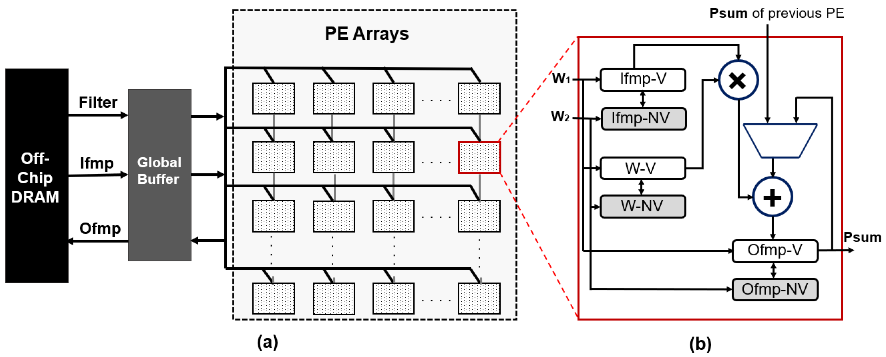
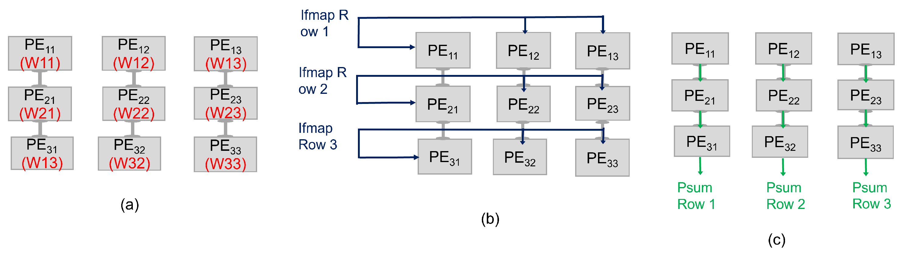
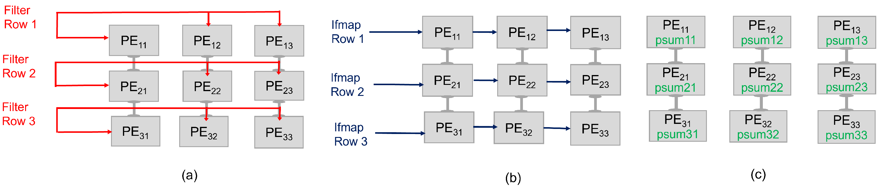
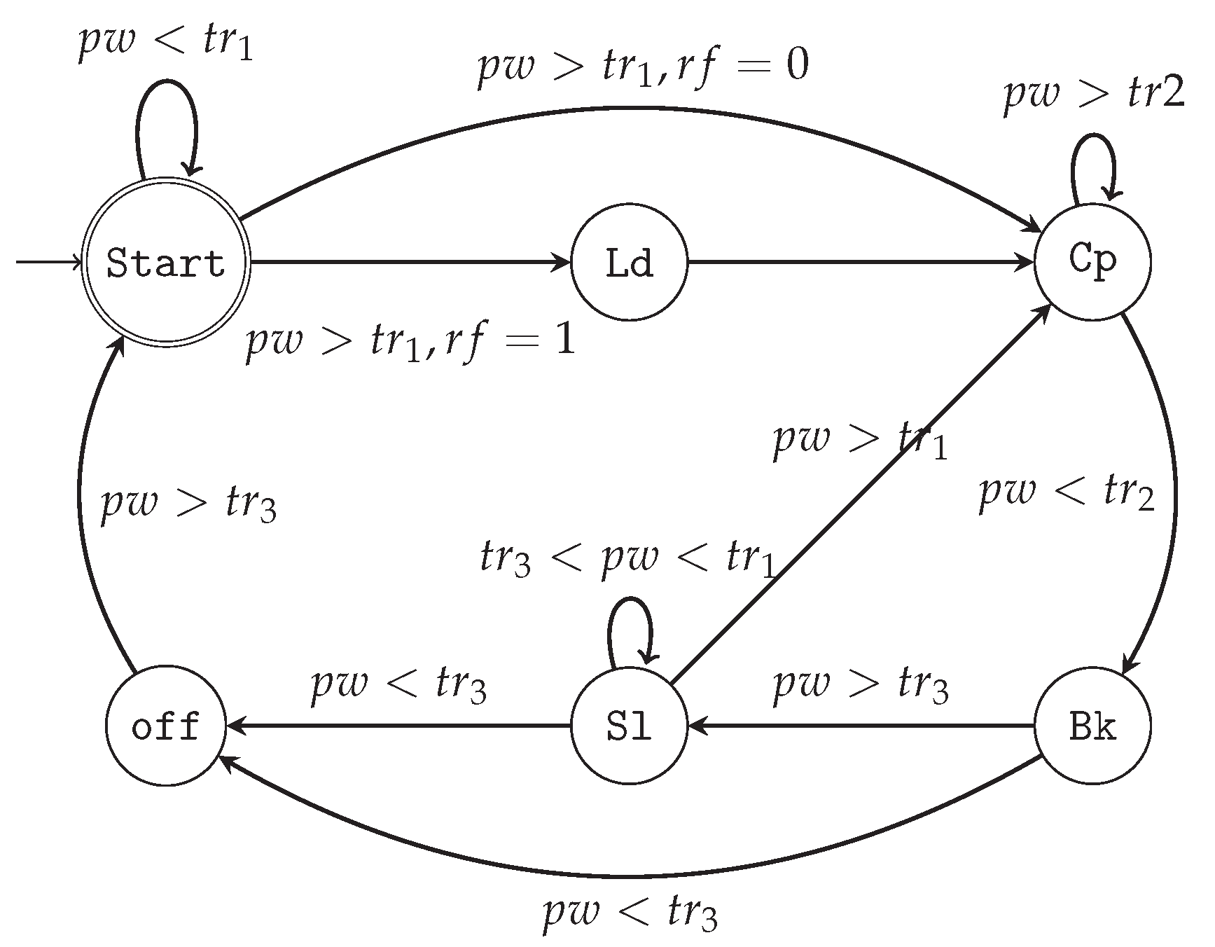
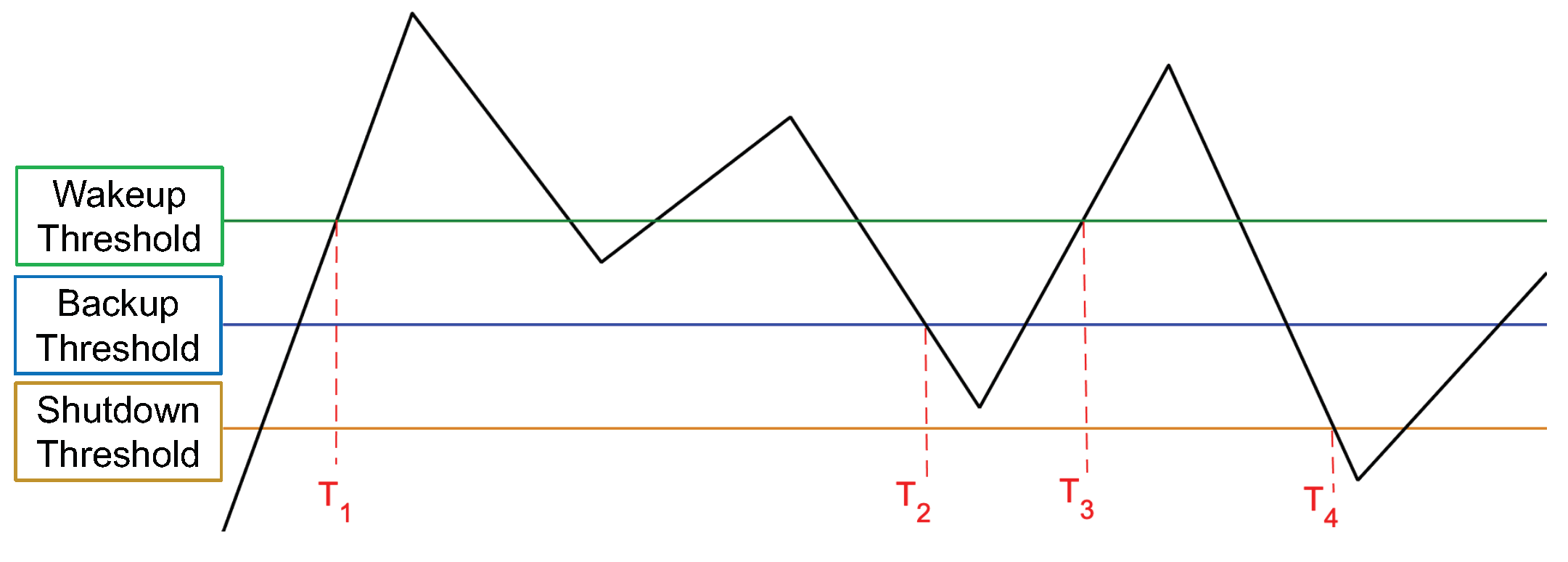
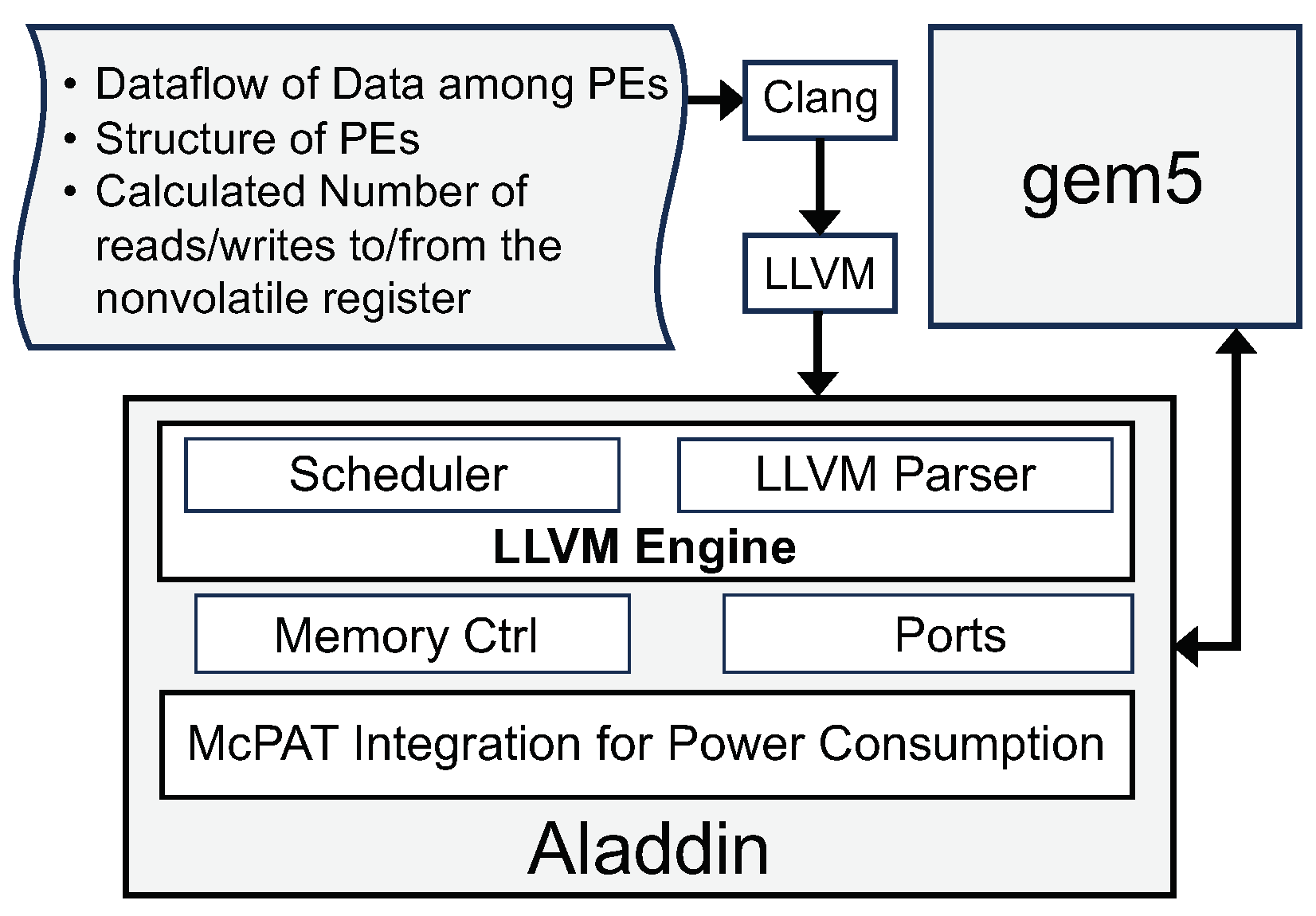
3. Proposed Intermittent-Aware Design Exploration
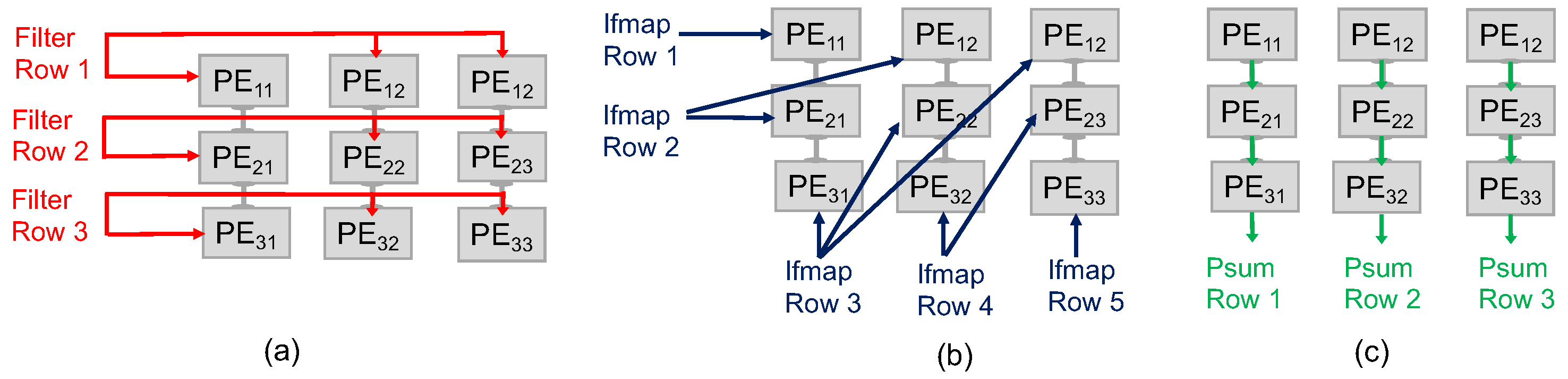
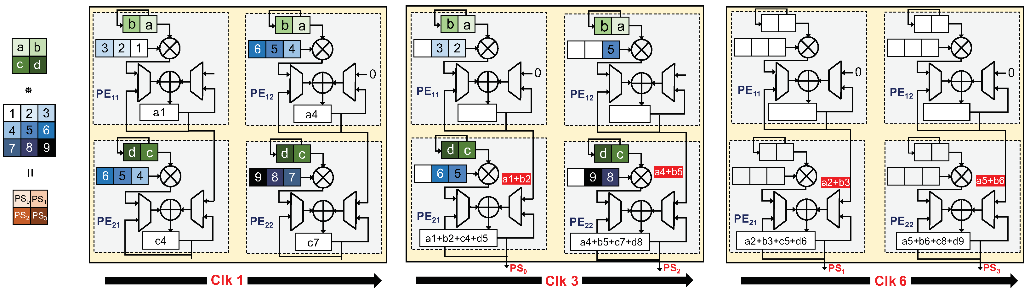
Architecture Behaviour
4. Evaluation Platform
4.1. Experimental Setup
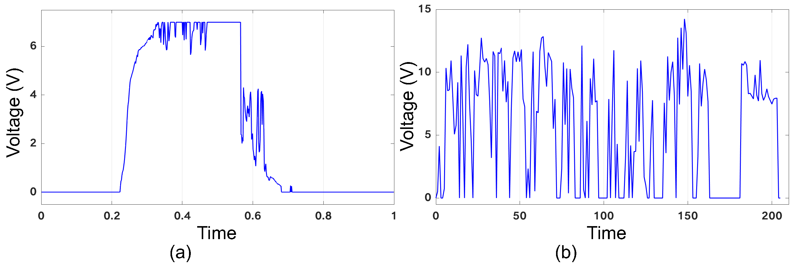
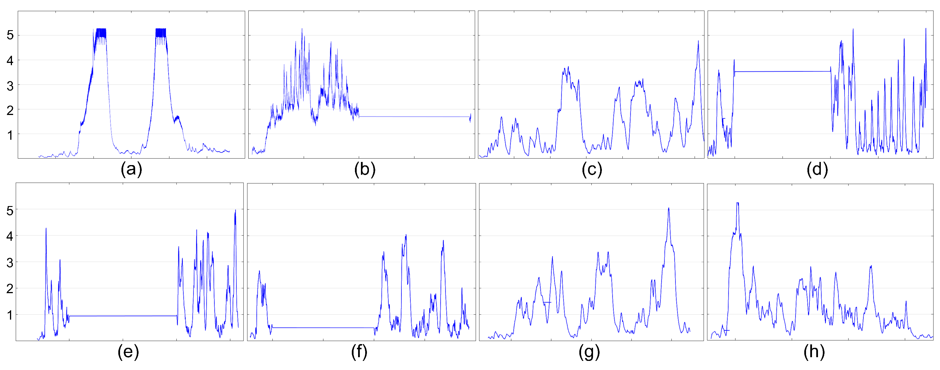
4.2. Non-Volatility and Intermittency Behaviors
4.3. Proof-of-Concept: AlexNet on CIFAR10
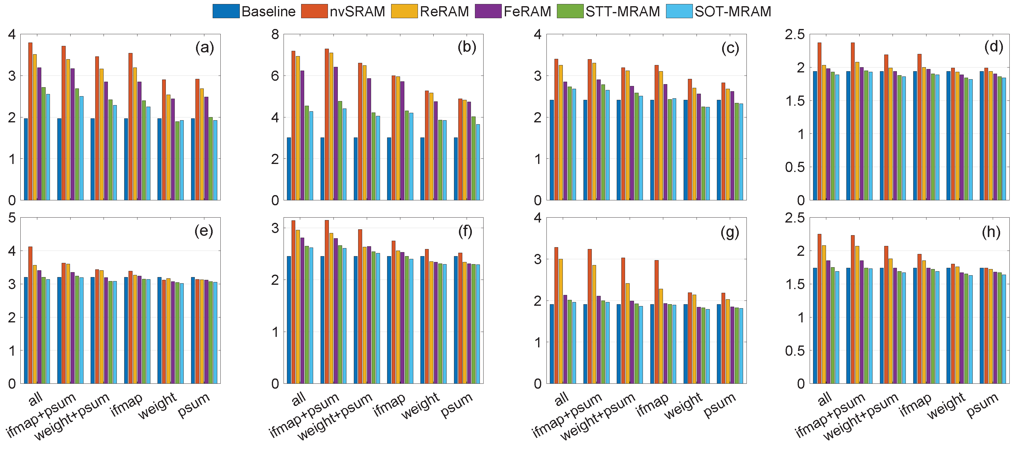
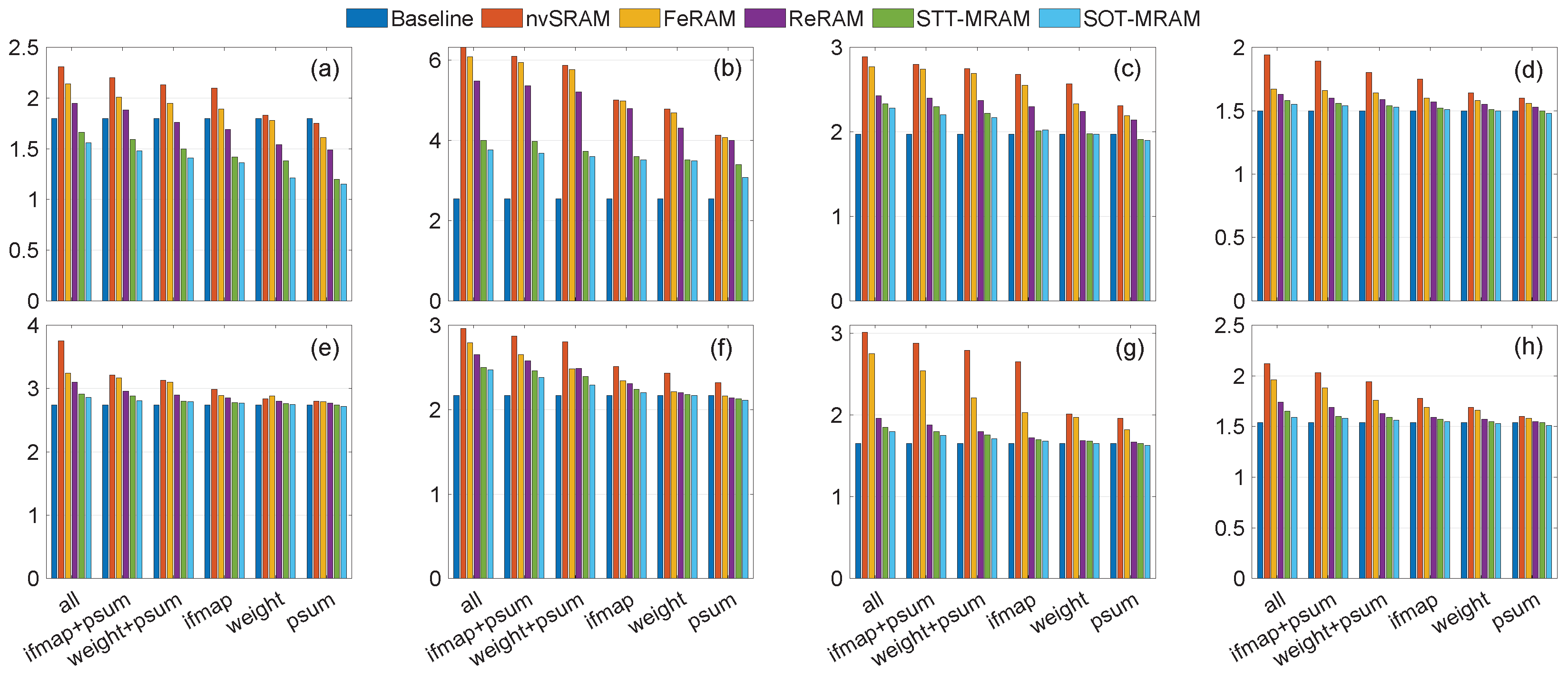
4.4. Performance Evaluation
5. Discussion and Future Work
5.1. Observation 1
5.2. Observation 2
5.3. Future Work
6. Conclusions
Author Contributions
Funding
Data Availability Statement
Conflicts of Interest
Abbreviations
| NVM | Non-volatile memory |
| PE | Processing Element |
| ASIC | Application-specific integrated circuit |
| CNN | Convolutional Neural Networks |
| MAC | Multiplication-and-Accumulation |
| ifmap | Input Feature Map |
| ofmap | Output Feature Map |
| W | Weight |
| WS | Weight Stationary |
| OS | Output Stationary |
| RS | Row Stationary |
| GLB | Global Buffer |
| CHRT | Cascaded Hierarchical Remanence Timekeepe |
| ReRAM | Resistive Random Access Memory |
| FeRAM | Ferroelectric RAM |
| nvSRAM | Non-Volatile Random Access Memory |
| SOT-MRAM | Spin-Orbit Torque Magnetic Random Access Memory |
| STT-MRAM | Spin-Transfer Torque Magnetic Random Access Memory |
References
- Awad, O.M.; Mahmoud, M.; Edo, I.; Zadeh, A.H.; Bannon, C.; Jayarajan, A.; Pekhimenko, G.; Moshovos, A. FPRaker: A processing element for accelerating neural network training. In Proceedings of the MICRO-54: 54th Annual IEEE/ACM MICRO, Virtual, 18–22 October 2021; pp. 857–869. [Google Scholar]
- Melchert, J.; Feng, K.; Donovick, C.; Daly, R.; Sharma, R.; Barrett, C.W.; Horowitz, M.; Hanrahan, P.M.; Raina, P. APEX: A Framework for Automated Processing Element Design Space Exploration using Frequent Subgraph Analysis. In Proceedings of the 28th ACM ASPLOS, Vancouver, BC, Canada, 25–29 March 2023; Volume 3, pp. 33–45. [Google Scholar]
- Maeng, K.; Lucia, B. Adaptive Dynamic Checkpointing for Safe Efficient Intermittent Computing. In Proceedings of the OSDI, Carlsbad, CA, USA, 8–10 October 2018; Volume 18, pp. 129–144. [Google Scholar]
- Surbatovich, M.; Lucia, B.; Jia, L. Towards a formal foundation of intermittent computing. Proc. ACM Program. Lang. 2020, 4, 1–31. [Google Scholar] [CrossRef]
- Silva, J.L.E.; Lopes, J.J. A dynamic dataflow architecture using partial reconfigurable hardware as an option for multiple cores. WSEAS Trans. Comput. 2010, 9, 429–444. [Google Scholar]
- Reuther, A.; Michaleas, P.; Jones, M.; Gadepally, V.; Samsi, S.; Kepner, J. AI accelerator survey and trends. In Proceedings of the 2021 IEEE HPEC, Waltham, MA, USA, 20–24 September 2021; pp. 1–9. [Google Scholar]
- Challapalle, N.; Rampalli, R.; Song, L.; Chandramoorthy, N.; Swaminathan, K.; Sampson, J.; Chen, Y.; Narayanan, V. GaaS-X: Graph analytics accelerator supporting sparse data representation using crossbar architectures. In Proceedings of the 2020 ACM/IEEE 47th ISCA, Valencia, Spain, 30 May–3 June 2020; pp. 433–445. [Google Scholar]
- Roohi, A.; Sheikhfaal, S.; Angizi, S.; Fan, D.; DeMara, R.F. Apgan: Approximate gan for robust low energy learning from imprecise components. IEEE Trans. Comput. 2019, 69, 349–360. [Google Scholar] [CrossRef]
- Roohi, A.; Angizi, S.; Fan, D.; DeMara, R.F. Processing-in-memory acceleration of convolutional neural networks for energy-effciency, and power-intermittency resilience. In Proceedings of the 20th International Symposium on Quality Electronic Design (ISQED), Santa Clara, CA, USA, 6–7 March 2019; pp. 8–13. [Google Scholar]
- Akella, A.; Saini, R.; Sharma, M.P. Social, economical and environmental impacts of renewable energy systems. Renew. Energy 2009, 34, 390–396. [Google Scholar] [CrossRef]
- Sharma, A. A comprehensive study of solar power in India and World. Renew. Sustain. Energy Rev. 2011, 15, 1767–1776. [Google Scholar] [CrossRef]
- Ferdous, R.M.; Reza, A.W.; Siddiqui, M.F. Renewable energy harvesting for wireless sensors using passive RFID tag technology: A review. Renew. Sustain. Energy Rev. 2016, 58, 1114–1128. [Google Scholar] [CrossRef]
- Eriksson, J.; Dunkels, A.; Finne, N.; Osterlind, F.; Voigt, T. Mspsim—An extensible simulator for msp430-equipped sensor boards. In Proceedings of the EWSN, Delft, The Netherlands, 29–31 January 2007; Volume 118. [Google Scholar]
- Roohi, A. Normally-off computing design methodology using spintronics: From device to architectures. In Proceedings of the 2020 11th International Green and Sustainable Computing Workshops (IGSC), Pullman, WA, USA, 19–22 October 2020; pp. 1–4. [Google Scholar]
- Roohi, A.; DeMara, R.F. NV-clustering: Normally-off computing using non-volatile datapaths. IEEE Trans. Comput. 2018, 67, 949–959. [Google Scholar] [CrossRef]
- Kreier. Solarmeter. 2020. Available online: https://github.com/kreier/solarmeter (accessed on 3 June 2023).
- Hester, J.; Sorber, J. The future of sensing is batteryless, intermittent, and awesome. In Proceedings of the 15th ACM Conference on Embedded Network Sensor Systems, Delft, The Netherlands, 6–8 November 2017; pp. 1–6. [Google Scholar]
- Singla, P.; Sarangi, S.R. A survey and experimental analysis of checkpointing techniques for energy harvesting devices. J. Syst. Archit. 2022, 126, 102464. [Google Scholar] [CrossRef]
- Lee, H.P.; Tseng, K.-Y.; Su, P. Interface discrete trap induced variability for negative capacitance FinFETs. In Proceedings of the 2018 International Symposium on VLSI-TSA, Hsinchu, Taiwan, 16–19 April 2018; pp. 1–2. [Google Scholar]
- Ruffini, S.; Caronti, L.; Yıldırım, K.S.; Brunelli, D. NORM: An FPGA-based non-volatile memory emulation framework for intermittent computing. ACM JETC 2022, 18, 1–18. [Google Scholar] [CrossRef]
- Bazzi, H.; Harb, A.; Aziza, H.; Moreau, M. Non-volatile SRAM memory cells based on ReRAM technology. SN Appl. Sci. 2020, 2, 1485. [Google Scholar] [CrossRef]
- Chen, W.; Qi, Z.; Akhtar, Z.; Siddique, K. Resistive-RAM-Based In-Memory Computing for Neural Network: A Review. Electronics 2022, 11, 3667. [Google Scholar] [CrossRef]
- Chien, T.K.; Chiou, L.-Y.; Sheu, S.-S.; Lin, J.-C.; Lee, C.-C.; Ku, T.-K.; Tsai, M.-J.; Wu, C.-I. Low-power MCU with embedded ReRAM buffers as sensor hub for IoT applications. IEEE JETCAS 2016, 6, 247–257. [Google Scholar] [CrossRef]
- Maciel, N.; Marques, E.; Naviner, L.; Zhou, Y.; Cai, H. Magnetic tunnel junction applications. Sensors 2019, 20, 121. [Google Scholar] [CrossRef]
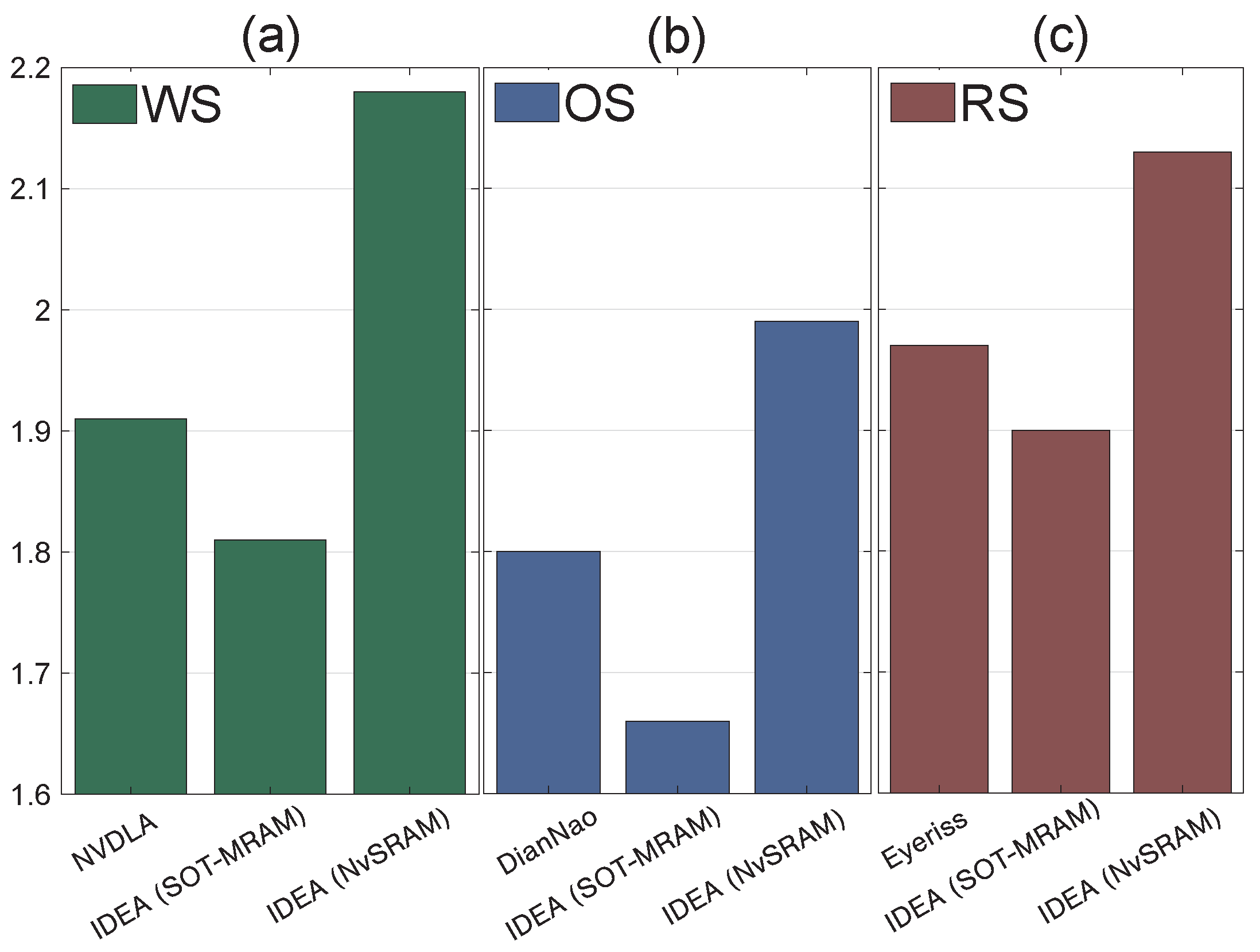
- Chen, Y.H.; Krishna, T.; Emer, J.S.; Sze, V. Eyeriss: An Energy-Efficient Reconfigurable Accelerator for Deep Convolutional Neural Networks. IEEE JSSC 2017, 52, 127–138. [Google Scholar] [CrossRef]
- Lee, J.; Mukhanov, L.; Molahosseini, A.S.; Minhas, U.; Hua, Y.; Martinez del Rincon, J.; Dichev, K.; Hong, C.H.; Vandierendonck, H. Resource-efficient convolutional networks: A survey on model-, arithmetic-, and implementation-level techniques. ACM Comput. Surv. 2023, 55, 1–36. [Google Scholar] [CrossRef]
- Silvano, C.; Ielmini, D.; Ferrandi, F.; Fiorin, L.; Curzel, S.; Benini, L.; Conti, F.; Garofalo, A.; Zambelli, C.; Calore, E.; et al. A survey on deep learning hardware accelerators for heterogeneous hpc platforms. arXiv 2023, arXiv:2306.15552. [Google Scholar]
- Lu, Z.; Cheng, R.; Jin, Y.; Tan, K.C.; Deb, K. Neural architecture search as multiobjective optimization benchmarks: Problem formulation and performance assessment. IEEE Trans. Evol. Comput. 2023. [Google Scholar] [CrossRef]
- Wu, Y.N.; Tsai, P.A.; Parashar, A.; Sze, V.; Emer, J.S. Sparseloop: An analytical approach to sparse tensor accelerator modeling. In Proceedings of the 2022 55th IEEE/ACM International Symposium on Microarchitecture (MICRO), Chicago, IL, USA, 1–5 October 2022; pp. 1377–1395. [Google Scholar]
- Reshadi, M.; Gregg, D. LOCAL: Low-complex mapping algorithm for spatial dnn accelerators. In Proceedings of the 2021 IEEE Nordic Circuits and Systems Conference (NorCAS), Oslo, Norway, 26–27 October 2021; pp. 1–7. [Google Scholar]
- NVIDIA. NVDLA Architecture. 2023. Available online: http://nvdla.org/hw/v1/hwarch.html (accessed on 26 December 2023).
- Reshadi, M.; Gregg, D. Dynamic Resource Partitioning for Multi-Tenant Systolic Array Based DNN Accelerator. In Proceedings of the 2023 31st Euromicro International Conference on Parallel, Distributed and Network-Based Processing (PDP), Naples, Italy, 1–3 March 2023; pp. 76–83. [Google Scholar]
- Qin, E.; Samajdar, A.; Kwon, H.; Nadella, V.; Srinivasan, S.; Das, D.; Kaul, B.; Krishna, T. Sigma: A sparse and irregular gemm accelerator with flexible interconnects for dnn training. In Proceedings of the 2020 IEEE International Symposium on High Performance Computer Architecture (HPCA), San Diego, CA, USA, 22–26 February 2020; pp. 58–70. [Google Scholar]
- Maron, H.; Fetaya, E.; Navon, A.; Shamsian, A.; Achituve, I.; Chechik, G. Designing Deep Networks to Process Other Deep Networks. 2023. Available online: https://developer.nvidia.com/blog/designing-deep-networks-to-process-other-deep-networks/ (accessed on 3 June 2023).
- Farabet, C.; Martini, B.; Corda, B.; Akselrod, P.; Culurciello, E.; LeCun, Y. Neuflow: A runtime reconfigurable dataflow processor for vision. In Proceedings of the CVPR 2011 Workshops, Colorado Springs, CO, USA, 20–25 June 2011; pp. 109–116. [Google Scholar]
- Knappe, G.A.; Wamhoff, E.C.; Bathe, M. Functionalizing DNA origami to investigate and interact with biological systems. Nat. Rev. Mater. 2023, 8, 123–138. [Google Scholar] [CrossRef]
- Kwon, H.; Chatarasi, P.; Pellauer, M.; Parashar, A.; Sarkar, V.; Krishna, T. Understanding reuse, performance, and hardware cost of dnn dataflow: A data-centric approach. In Proceedings of the 52nd Annual IEEE/ACM International Symposium on Microarchitecture, Columbus, OH, USA, 12–16 October 2019; pp. 754–768. [Google Scholar]
- Xu, R.; Ma, S.; Guo, Y.; Li, D. A Survey of Design and Optimization for Systolic Array Based DNN Accelerators. ACM Comput. Surv. 2023, 56, 1–17. [Google Scholar] [CrossRef]
- Zhao, Z.; Cao, R.; Un, K.F.; Yu, W.H.; Mak, P.I.; Martins, R.P. An fpga-based transformer accelerator using output block stationary dataflow for object recognition applications. IEEE Trans. Circuits Syst. II Express Briefs 2022, 70, 281–285. [Google Scholar] [CrossRef]
- Du, Z.; Fasthuber, R.; Chen, T.; Ienne, P.; Li, L.; Luo, T.; Feng, X.; Chen, Y.; Temam, O. ShiDianNao: Shifting vision processing closer to the sensor. In Proceedings of the 42nd Annual International Symposium on Computer Architecture, Portland, OR, USA, 13–17 June 2015; pp. 92–104. [Google Scholar]
- Li, Y.; Zhao, J.; Qianqi, S.; Mai, H.; Chen, L.; Cao, W.; Chen, Y.; Liu, Y.; Zhang, X.; Shi, X.; et al. SIRIUS: Harvesting Whole-Program Optimization Opportunities for DNNs. Proc. Mach. Learn. Syst. 2023, 5, 1–17. [Google Scholar]
- Zhang, X. The AlexNet, LeNet-5 and VGG NET applied to CIFAR-10. In Proceedings of the 2021 2nd IICBASE, Zhuhai, China, 24–26 September 2021; pp. 414–419. [Google Scholar]
- Zhang, X.; Song, J.; Wang, Y.; Zhang, Y.; Zhang, Z.; Wang, R.; Huang, R. An Energy-Efficient Mixed-Signal Parallel Multiply-Accumulate (MAC) Engine Based on Stochastic Computing. arXiv 2019, arXiv:1907.01807. [Google Scholar]
- Furlong, M.; Hester, J.; Storer, K.; Sorber, J. Realistic simulation for tiny batteryless sensors. In Proceedings of the 4th International Workshop on Energy Harvesting and Energy-Neutral Sensing Systems, Stanford, CA, USA, 14–16 November 2016; pp. 23–26. [Google Scholar]
- Raibabar. Classification Model: LeNet and AlexNet on CIFAR-10. 2023. Available online: https://www.kaggle.com/code/raibabar/classification-model-lenet-and-alexnet-on-cifar10 (accessed on 3 June 2023).
- Shao, Y.S.; Xi, S.L.; Srinivasan, V.; Wei, G.-Y.; Brooks, D. Co-designing accelerators and SoC interfaces using gem5-Aladdin. In Proceedings of the 2016 49th Annual IEEE/ACM MICRO, Taipei, Taiwan, 15–19 October 2016; pp. 1–12. [Google Scholar] [CrossRef]


| Technology | nvSRAM [21] | ReRAM [22] | FeRAM [23] | STT-MRAM [24] | SOT-MRAM [24] |
|---|---|---|---|---|---|
| Read time (ns) | 0.22 | 5 | 60 | 5 | 10 |
| Write time (ns) | 0.24 | 5 | 60 | 10 | 1 |
| Read energy (fJ) | 50 | 2700 | 9000 | 10 | 10 |
| Write energy (fJ) | 3000 | 2700 | 9000 | 100 | 10 |
| Read Power (mW) | 0.22 | 0.54 | 0.15 | 0.002 | 0.001 |
| Write Power (mW) | 12.5 | 0.54 | 0.15 | 0.01 | 0.01 |
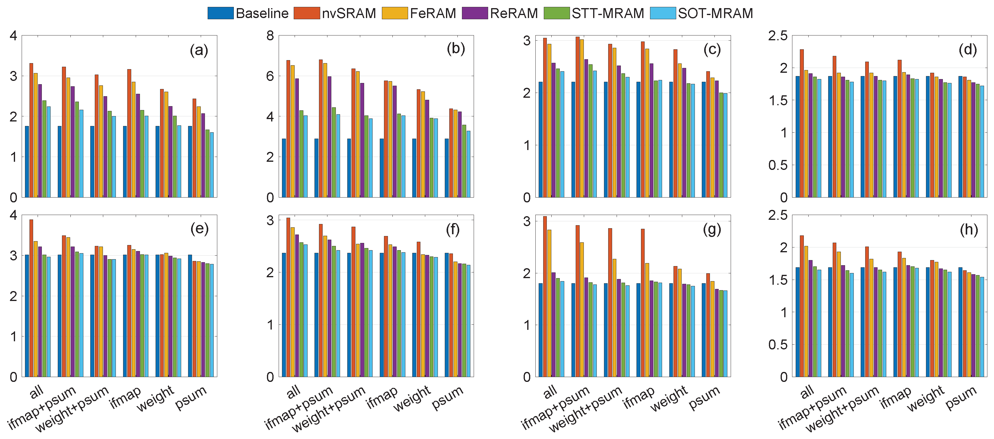
| Trace in Figure 10 | Baseline | NVM-Enhanced IDEA | Improvement (%) | ||||
|---|---|---|---|---|---|---|---|
| RS | OS | WS | RS | OS | WS | ||
| (a) | 2276 | 1748 | 1935 | 2048 | 23.16 | 14.9 | 10 |
| (b) | 7813 | 7715 | 7731 | 7780 | 1.25 | 1.04 | 0.42 |
| (c) | 5117 | 3525 | 4349 | 4505 | 31.10 | 15 | 11.9 |
| (d) | 3564 | 2930 | 3046 | 3194 | 17.80 | 14.6 | 10.38 |
| (e) | 8038 | 6010 | 6398 | 6787 | 25.19 | 20.4 | 15.56 |
| (f) | 6561 | 5103 | 5477 | 5801 | 22.22 | 16.52 | 11.58 |
| (g) | 4019 | 3364 | 3571 | 3784 | 16.3 | 11.14 | 5.84 |
| (h) | 3753 | 2943 | 3103 | 3309 | 21.58 | 17.37 | 11.83 |
Disclaimer/Publisher’s Note: The statements, opinions and data contained in all publications are solely those of the individual author(s) and contributor(s) and not of MDPI and/or the editor(s). MDPI and/or the editor(s) disclaim responsibility for any injury to people or property resulting from any ideas, methods, instructions or products referred to in the content. |
© 2024 by the authors. Licensee MDPI, Basel, Switzerland. This article is an open access article distributed under the terms and conditions of the Creative Commons Attribution (CC BY) license (https://creativecommons.org/licenses/by/4.0/).
Share and Cite
Taheri, N.; Tabrizchi, S.; Roohi, A. Intermittent-Aware Design Exploration of Systolic Array Using Various Non-Volatile Memory: A Comparative Study. Micromachines 2024, 15, 343. https://doi.org/10.3390/mi15030343
Taheri N, Tabrizchi S, Roohi A. Intermittent-Aware Design Exploration of Systolic Array Using Various Non-Volatile Memory: A Comparative Study. Micromachines. 2024; 15(3):343. https://doi.org/10.3390/mi15030343
Chicago/Turabian StyleTaheri, Nedasadat, Sepehr Tabrizchi, and Arman Roohi. 2024. "Intermittent-Aware Design Exploration of Systolic Array Using Various Non-Volatile Memory: A Comparative Study" Micromachines 15, no. 3: 343. https://doi.org/10.3390/mi15030343