
Research on the Reliability of Threshold Voltage Based on GaN High-Electron-Mobility Transistors

Abstract
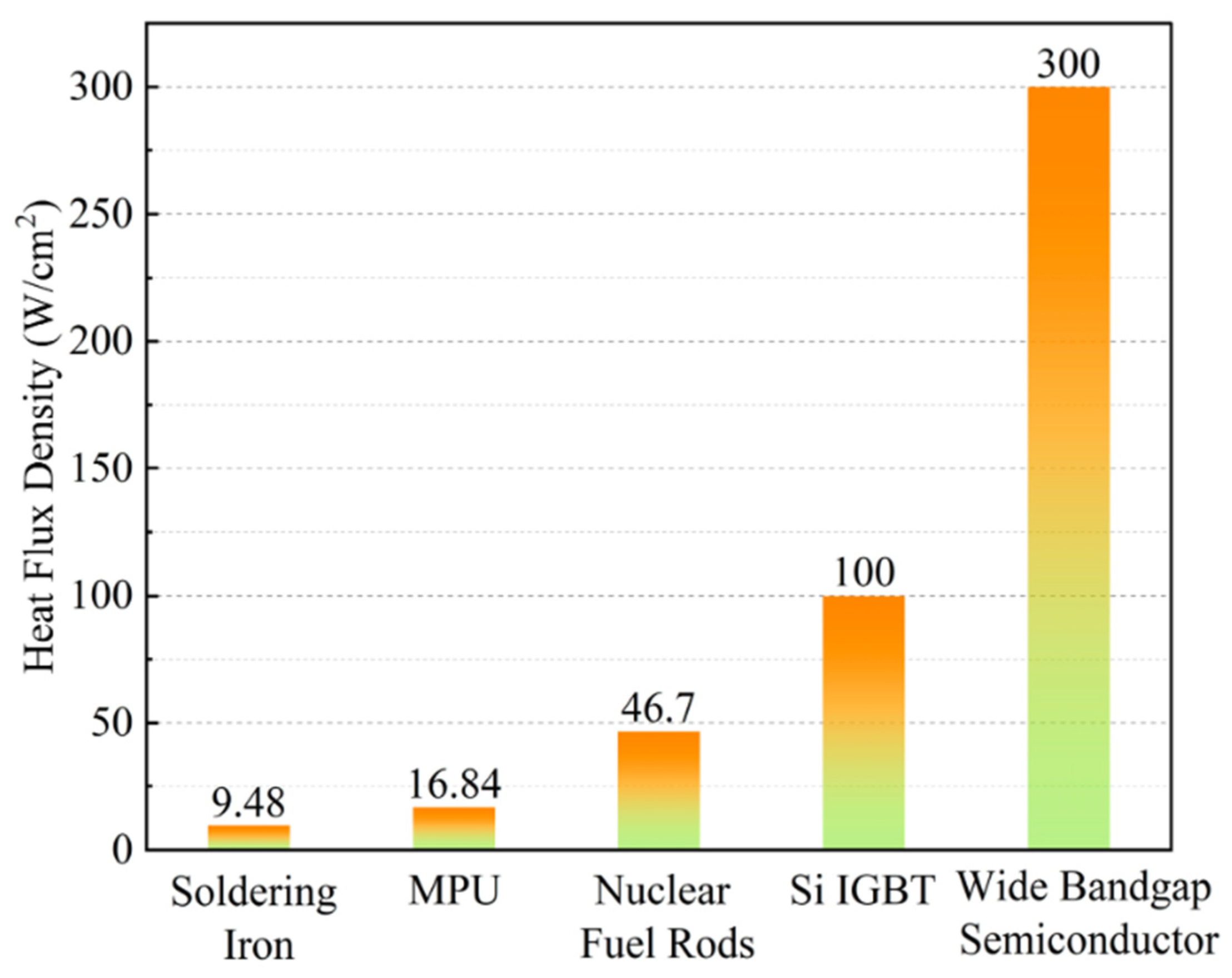
:1. Introduction
2. Factors Affecting VTH Drift
2.1. Effect of Switching Stress
2.2. Effects of Thermal Stress
3. Reasons for VTH Drift
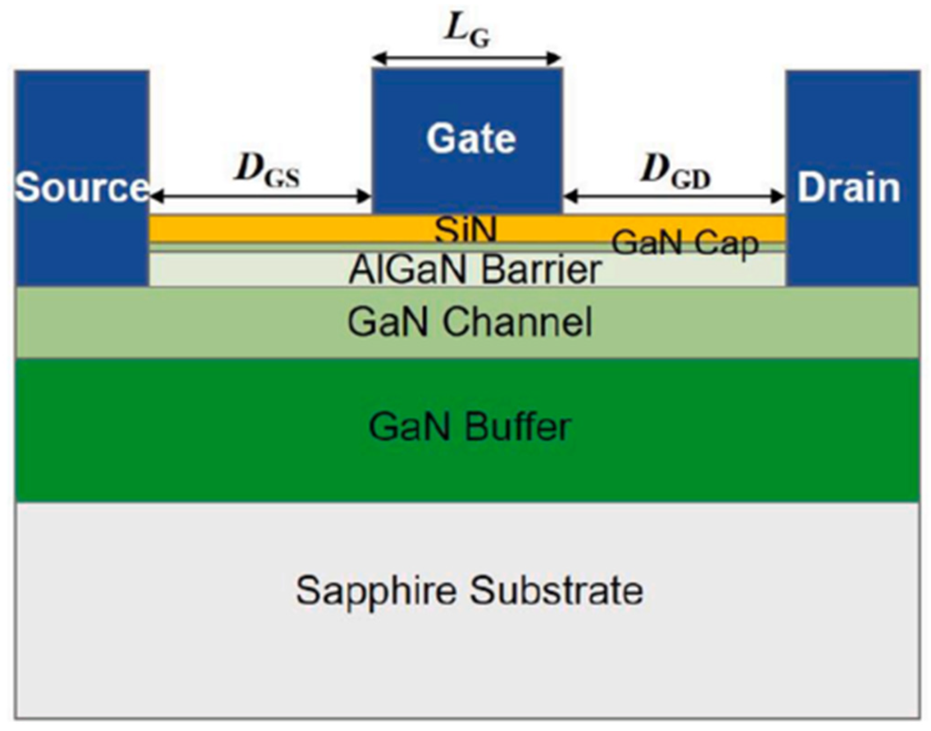
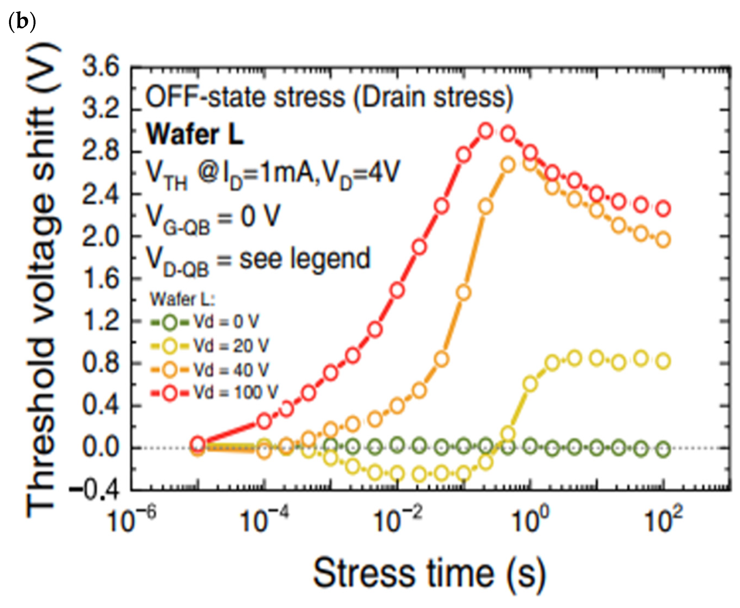
3.1. Analysis of Switching Stresses
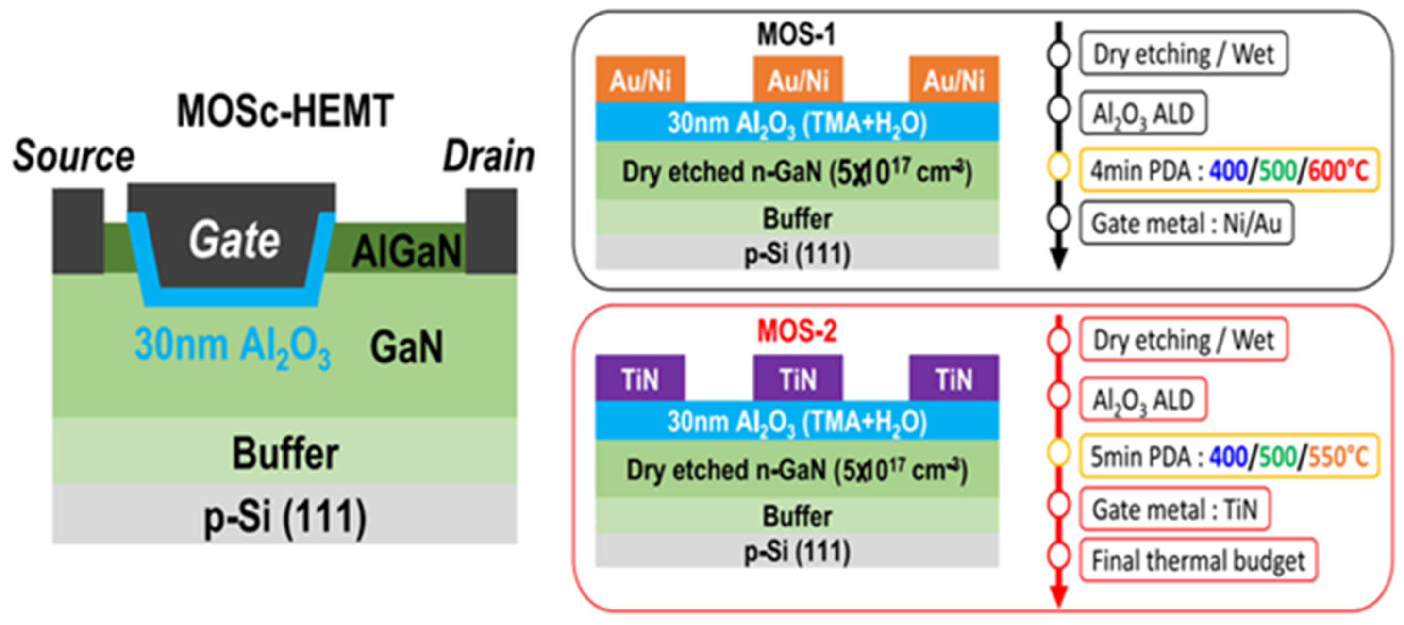
3.2. Analysis of Thermal Stress
4. Conclusions and Future Perspectives
Author Contributions
Funding
Data Availability Statement
Acknowledgments
Conflicts of Interest
References
- Khandelwal, S.; Goyal, N.; Fjeldly, T.A. A Physics-Based Analytical Model for 2DEG Charge Density in AlGaN/GaN HEMT Devices. IEEE Trans. Electron Devices 2011, 58, 3622–3625. [Google Scholar] [CrossRef]
- Swamy, N.S.; Dutta, A.K. Analytical Models for the 2DEG Density, AlGaN Layer Carrier Density, and Drain Current for AlGaN/GaN HEMTs. IEEE Trans. Electron Devices 2018, 65, 936–944. [Google Scholar] [CrossRef]
- Shi, Y.; Chen, W.; Sun, R.; Liu, C.; Xin, Y.; Xia, Y.; Wang, F.; Xu, X.; Deng, X.; Chen, T.; et al. Modeling the Influence of the Acceptor-Type Trap on the 2DEG Density for GaN MIS-HEMTs. IEEE Trans. Electron Devices 2020, 67, 2290–2296. [Google Scholar] [CrossRef]
- Lee, D.S.; Gao, X.; Guo, S.; Kopp, D.; Fay, P.; Palacios, T. 300-GHz InAlN/GaN HEMTs With InGaN Back Barrier. IEEE Electron Device Lett. 2011, 32, 1525–1527. [Google Scholar] [CrossRef]
- Miller, N.C.; Brown, A.; Elliott, M.; Gilbert, R.; Davis, D.T.; Islam, A.E.; Walker, D.; Hughes, G.; Liddy, K.; Chabak, K.D. An ASM-HEMT for Large-Signal Modeling of GaN HEMTs in High-Temperature Applications. IEEE J. Electron Devices Soc. 2023, 11, 531–538. [Google Scholar] [CrossRef]
- Sahebghalam, N.; Shalchian, M.; Chalechale, A.; Jazaeri, F. High-Temperature HEMT Model. IEEE Trans. Electron Devices 2022, 69, 4821–4827. [Google Scholar] [CrossRef]
- Khan, A.K.; Alim, M.A.; Gaquiere, C. 2DEG transport properties over temperature for AlGaN/GaN HEMT and AlGaN/InGaN/GaN pHEMT. Microelectron. Eng. 2021, 238, 111508. [Google Scholar] [CrossRef]
- Wu, H.; Fu, X.; Guo, J.; Wang, Y.; Liu, T.; Hu, S. Time-Resolved Threshold Voltage Instability of 650-V Schottky Type p-GaN Gate HEMT under Temperature-Dependent Forward and Reverse Gate Bias Conditions. IEEE Trans. Electron Devices 2022, 69, 531–535. [Google Scholar] [CrossRef]
- Nuo, M.; Wu, Y.; Yang, J.; Hao, Y.; Wang, M.; Wei, J. Time-Resolved Extraction of Negatively Shifted Threshold Voltage in Schottky-Type p-GaN Gate HEMT Biased at High VDS. IEEE Trans. Electron Devices 2023, 70, 3462–3467. [Google Scholar] [CrossRef]
- Uemoto, Y.; Hikita, M.; Ueno, H.; Matsuo, H.; Ishida, H.; Yanagihara, M.; Ueda, T.; Tanaka, T.; Ueda, D. Gate injection transistor (GIT)—A normally-off AlGaN/GaN power transistor using conductivity modulation. IEEE Trans. Electron Devices 2007, 54, 3393–3399. [Google Scholar] [CrossRef]
- Zhong, Y.; Su, S.; Chen, X.; Zhou, Y.; He, J.; Gao, H.; Zhan, X.; Guo, X.; Liu, J.; Sun, Q.; et al. Normally-off HEMTs with regrown p-GaN gate and low-pressure chemical vapor deposition SiNx passivation by using an AlN pre-layer. IEEE Electron Device Lett. 2019, 40, 1495–1498. [Google Scholar] [CrossRef]
- Wei, J.; Xie, R.; Xu, H.; Wang, H.; Wang, Y.; Hua, M.; Zhong, K.; Tang, G.; He, J.; Zhang, M.; et al. Charge storage mechanism of drain induced dynamic threshold voltage shift in p-GaN gate HEMTs. IEEE Electron Device Lett. 2019, 40, 526–529. [Google Scholar] [CrossRef]
- Wei, J.; Xu, H.; Xie, R.; Zhang, M.; Wang, H.; Wang, Y.; Zhong, K.; Hua, M.; He, J.; Chen, K.J. Dynamic threshold voltage in p-GaN gate HEMT. In Proceedings of the 2019 31st International Symposium on Power Semiconductor Devices and ICs (ISPSD), Shanghai, China, 19–23 May 2019; pp. 291–294. [Google Scholar]
- Tang, S.W.; Bakeroot, B.; Huang, Z.H.; Chen, S.C.; Lin, W.S.; Lo, T.C.; Borga, M.; Wellekens, D.; Posthuma, N.; Decoutere, S.; et al. Using Gate Leakage Conduction to Understand Positive Gate Bias Induced Threshold Voltage Shift in p-GaN Gate HEMTs. IEEE Trans. Electron Devices 2023, 70, 449–453. [Google Scholar] [CrossRef]
- Tang, S.W.; Lin, W.S.; Huang, Z.H.; Wu, T.L. Capacitance-Dependent VTH Instability Under a High dVg/dt Event in p-GaN Power HEMTs. IEEE Electron Device Lett. 2022, 43, 1617–1620. [Google Scholar] [CrossRef]
- Zhou, X.; Wang, Z.; Wu, Z.; Zhou, Q.; Qiao, M.; Li, Z.; Zhang, B. Total-Ionizing-Dose Radiation Effect on Dynamic Threshold Voltage in p-GaN Gate HEMTs. IEEE Trans. Electron Devices 2023, 70, 4081–4086. [Google Scholar] [CrossRef]
- Chen, J.; Su, Y.; Pan, C.; Kuang, W.; Yang, K.; Wang, H.; Wang, M.; Zhang, B.; Zhou, Q. The Device Instability of p-GaN Gate HEMTs Induced by Self-Heating Effect Investigated by on-State Drain Current Injection (DCI) Technique. IEEE Trans. Electron Devices 2022, 69, 5496–5502. [Google Scholar] [CrossRef]
- Lin, J.H.; Ciou, F.M.; Chang, T.C.; Lin, Y.S.; Hsu, J.T.; Jin, F.Y.; Chang, K.C.; Kuo, T.T.; Chen, K.H.; Hung, Y.H.; et al. Abnormal Threshold Voltage Degradation Under Semi-On State Stress in Si3N4/AlGaN/GaN-HEMT. IEEE Electron Device Lett. 2022, 43, 1420–1423. [Google Scholar] [CrossRef]
- Jiang, H.; Zhu, R.; Lyu, Q.; Lau, K.M. High-Voltage p-GaN HEMTs With OFF-State Blocking Capability After Gate Breakdown. IEEE Electron Device Lett. 2019, 40, 530–533. [Google Scholar] [CrossRef]
- Wang, H.; Wei, J.; Xie, R.; Liu, C.; Tang, G.; Chen, K.J. Maximizing the Performance of 650-V p-GaN Gate HEMTs: Dynamic RON Characterization and Circuit Design Considerations. IEEE Trans. Power Electron. 2017, 32, 5539–5549. [Google Scholar] [CrossRef]
- EPC2025 Datasheet, EPC. 2015. Available online: http://epc-co.com/epc (accessed on 10 October 2023).
- PGA26E19BA Datasheet, Panasonic, Osaka, Japan. 2015. Available online: http://www.mouser.hk (accessed on 10 October 2023).
- GS66504B Datasheet, GaN Systems, Ottawa, ON, Canada. 2015. Available online: http://www.gansystems.com (accessed on 10 October 2023).
- Rocha, P.F.P.P.; Vauche, L.; Mohamad, B.; Vandendaele, W.; Martinez, E.; Veillerot, M.; Spelta, T.; Rochat, N.; Gwoziecki, R.; Salem, B.; et al. Impact of post-deposition anneal on ALD Al2O3/etched GaN interface for gate-first MOSc-HEMT. Power Electron. Devices Compon. 2023, 4, 100033. [Google Scholar] [CrossRef]
- Yoon, Y.J.; Lee, J.S.; Kang, I.M.; Lee, E.J.; Kim, D.S. Impact of process-dependent SiNx passivation on proton-induced degradation in GaN MIS-HEMTs. Results Phys. 2021, 31, 105013. [Google Scholar] [CrossRef]
- Lee, J.H.; Kim, D.S.; Kim, J.G. Effect of gate dielectrics on characteristics of high-energy proton-irradiated AlGaN/GaN MISHEMTs. Radiat. Phys. Chem. 2021, 184, 109473. [Google Scholar] [CrossRef]
- Zhong, K.; Xu, H.; Zheng, Z.; Chen, J.; Chen, K.J. Characterization of Dynamic Threshold Voltage in Schottky-Type p-GaN Gate HEMT Under High-Frequency Switching. IEEE Electron Device Lett. 2021, 42, 501–504. [Google Scholar] [CrossRef]
- Chae, M.; Kim, H. Investigation of the Gate Degradation Induced by Forward Gate Voltage Stress in p-GaN Gate High Electron Mobility Transistors. Micromachines 2023, 14, 977. [Google Scholar] [CrossRef] [PubMed]
- Meneghini, M.; Hilt, O.; Wuerfl, J.; Meneghesso, G. Technology and reliability of normally-off GaN HEMTs with p-type gate. Energies 2017, 10, 153. [Google Scholar] [CrossRef]
- Efthymiou, L.; Murukesan, K.; Longobardi, G.; Udrea, F.; Shibib, A.; Terrill, K. Understanding the Threshold Voltage Instability During OFF-State Stress in p-GaN HEMTs. IEEE Electron Device Lett. 2019, 40, 1253–1256. [Google Scholar] [CrossRef]
- Sayadi, L.; Iannaccone, G.; Sicre, S.; Häberlen, O.; Curatola, G. Threshold Voltage Instability in p-GaN Gate AlGaN/GaN HFETs. IEEE Trans. Electron Devices 2018, 65, 2454–2460. [Google Scholar] [CrossRef]
- Lai, Y.C.; Zhong, Y.N. Gate Capacitance and Off-State Characteristics of E-Mode p-GaN Gate AlGaN/GaN High-Electron-Mobility Transistors After Gate Stress Bias. J. Electron. Mater. 2021, 50, 1162–1166. [Google Scholar] [CrossRef]
- Favero, D.; De Santi, C.; Stockman, A. Trade-off between gate leakage current and threshold voltage stability in power HEMTs during ON-state and OFF-state stress. Microelectron. Reliab. 2023, 150, 115129. [Google Scholar] [CrossRef]
- Amano, H.; Baines, Y.; Beam, E.; Borga, M.; Bouchet, T.; Chalker, P.R.; Charles, M.; Chen, K.J.; Chowdhury, N.; Chu, R.; et al. The 2018 GaN power electronics roadmap. J. Phys. D Appl. Phys. 2018, 51, 163001. [Google Scholar] [CrossRef]
- Chu, R. GaN power switches on the rise: Demonstrated benefits and unrealized potentials. Appl. Phys. Lett. 2020, 116, 090502. [Google Scholar] [CrossRef]
- Wang, K.; Zhu, Y.; Zhao, H.; Zhao, R.; Zhu, B. Steady-State Temperature-Sensitive Electrical Parameters’ Characteristics of GaN HEMT Power Devices. Electronics 2024, 13, 363. [Google Scholar] [CrossRef]
- Wang, H.; Lin, Y.; Jiang, J.; Dong, D.; Ji, F.; Zhang, M.; Jiang, M.; Gan, W.; Li, H.; Wang, M.; et al. Investigation of Thermally Induced Threshold Voltage Shift in Normally-OFF p-GaN Gate HEMTs. IEEE Trans. Electron Devices 2022, 69, 2287–2292. [Google Scholar] [CrossRef]
- Pilati, M.; Buffolo, M.; Rampazzo, F. Impact of high-temperature operating lifetime tests on the stability of 0.15 μm AlGaN/GaN HEMTs: A temperature-dependent analysis. Microelectron. Reliab. 2023, 150, 115131. [Google Scholar] [CrossRef]
- Tallarico, A.N.; Stoffels, S.; Magnone, P.; Posthuma, N.; Sangiorgi, E.; Decoutere, S.; Fiegna, C. Investigation of the p-GaN Gate Breakdown in Forward-Biased GaN-Based Power HEMTs. IEEE Electron Device Lett. 2017, 38, 99–102. [Google Scholar] [CrossRef]
- Shi, Y.; Zhou, Q.; Cheng, Q.; Wei, P.; Zhu, L.; Wei, D.; Zhang, A.; Chen, W.; Zhang, B. Carrier Transport Mechanisms Underlying the Bidirectional VTH Shift in p-GaN Gate HEMTs Under Forward Gate Stress. IEEE Trans. Electron Devices 2019, 66, 876–882. [Google Scholar] [CrossRef]
- Xu, R.; Chen, P.; Liu, X.; Zhao, J.; Zhu, T.; Chen, D.; Xie, Z.; Ye, J.; Xiu, X.; Wan, F.; et al. A Lateral AlGaN/GaN Schottky Barrier Diode with 0.36 V Turn-on Voltage and 10 kV Breakdown Voltage by Using Double Barrier Anode Structure. Chip 2023, 100079. [Google Scholar] [CrossRef]
- Sun, Y.; Wang, Y.; Tang, J.; Wang, W.; Huang, Y.; Kuang, X. A Breakdown Enhanced AlGaN/GaN Schottky Barrier Diode with the T-Anode Position Deep into the Bottom Buffer Layer. Micromachines 2019, 10, 91. [Google Scholar] [CrossRef] [PubMed]
- Lee, M.; Ahn, C.W.; Vu, T.K.O.; Lee, H.U.; Jeong, Y.; Hahm, M.G.; Kim, E.K.; Park, S. Current Transport Mechanism in Palladium Schottky Contact on Si-Based Freestanding GaN. Nanomaterials 2020, 10, 297. [Google Scholar] [CrossRef] [PubMed]
- Artur, L.; Ewa, G.; Robert, C. Effect of doping of layers surrounding GaN/InGaN multiple quantum wells on their thermal stability. Mater. Sci. Semicond. Process. 2023, 166, 107752. [Google Scholar]
- Huang, Z.H.; Sun, H.Q.; Ding, X. Novel gate air cavity GaN HEMTs design for improved RF and DC performance. Results Phys. 2021, 29, 104718. [Google Scholar] [CrossRef]


Disclaimer/Publisher’s Note: The statements, opinions and data contained in all publications are solely those of the individual author(s) and contributor(s) and not of MDPI and/or the editor(s). MDPI and/or the editor(s) disclaim responsibility for any injury to people or property resulting from any ideas, methods, instructions or products referred to in the content. |
© 2024 by the authors. Licensee MDPI, Basel, Switzerland. This article is an open access article distributed under the terms and conditions of the Creative Commons Attribution (CC BY) license (https://creativecommons.org/licenses/by/4.0/).
Share and Cite
Dai, P.; Wang, S.; Lu, H. Research on the Reliability of Threshold Voltage Based on GaN High-Electron-Mobility Transistors. Micromachines 2024, 15, 321. https://doi.org/10.3390/mi15030321
Dai P, Wang S, Lu H. Research on the Reliability of Threshold Voltage Based on GaN High-Electron-Mobility Transistors. Micromachines. 2024; 15(3):321. https://doi.org/10.3390/mi15030321
Chicago/Turabian StyleDai, Pengfei, Shaowei Wang, and Hongliang Lu. 2024. "Research on the Reliability of Threshold Voltage Based on GaN High-Electron-Mobility Transistors" Micromachines 15, no. 3: 321. https://doi.org/10.3390/mi15030321