
Wafer Surface Defect Detection Based on Background Subtraction and Faster R-CNN
Abstract
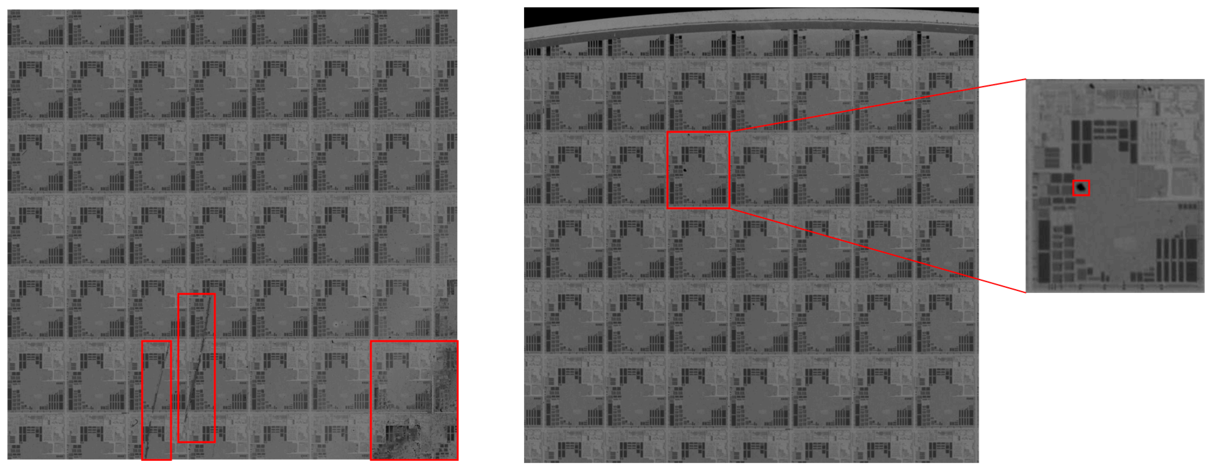
:1. Introduction
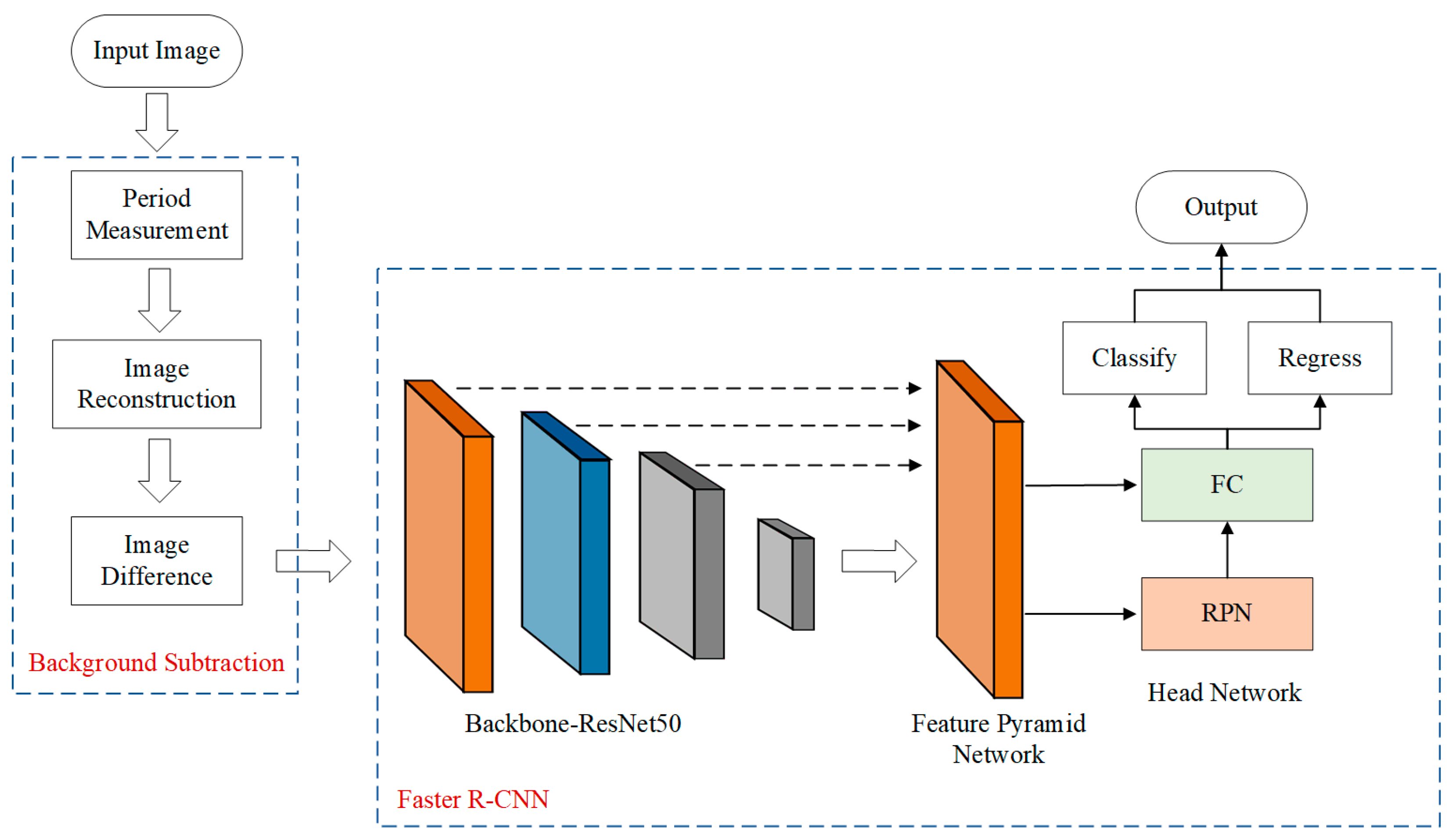
2. Wafer Surface Defect Detection Method
2.1. Solution Overview
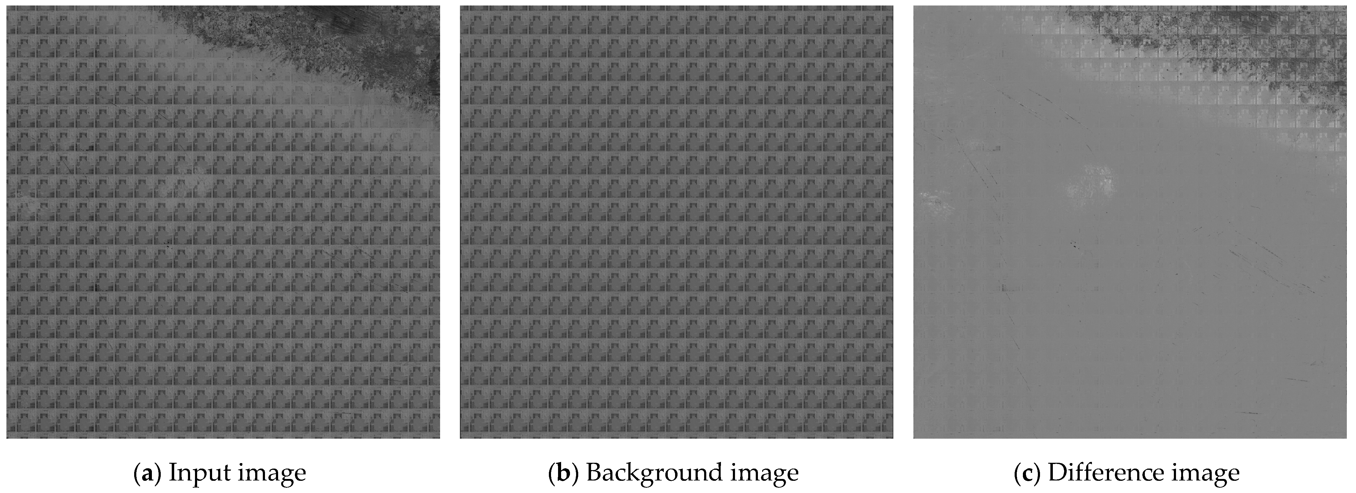
2.2. Background Subtraction
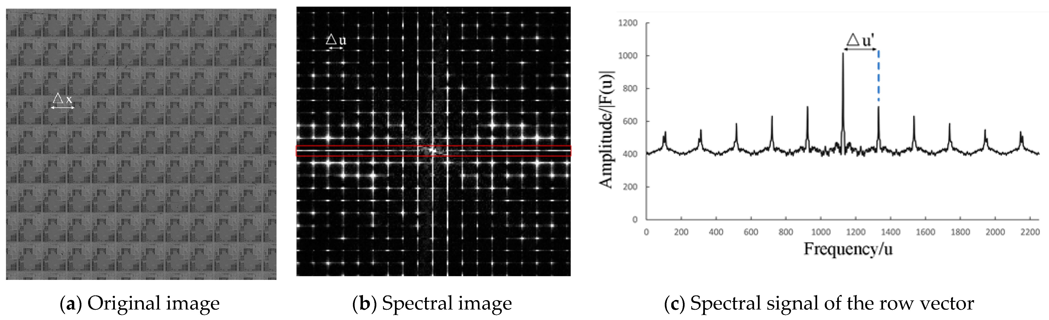
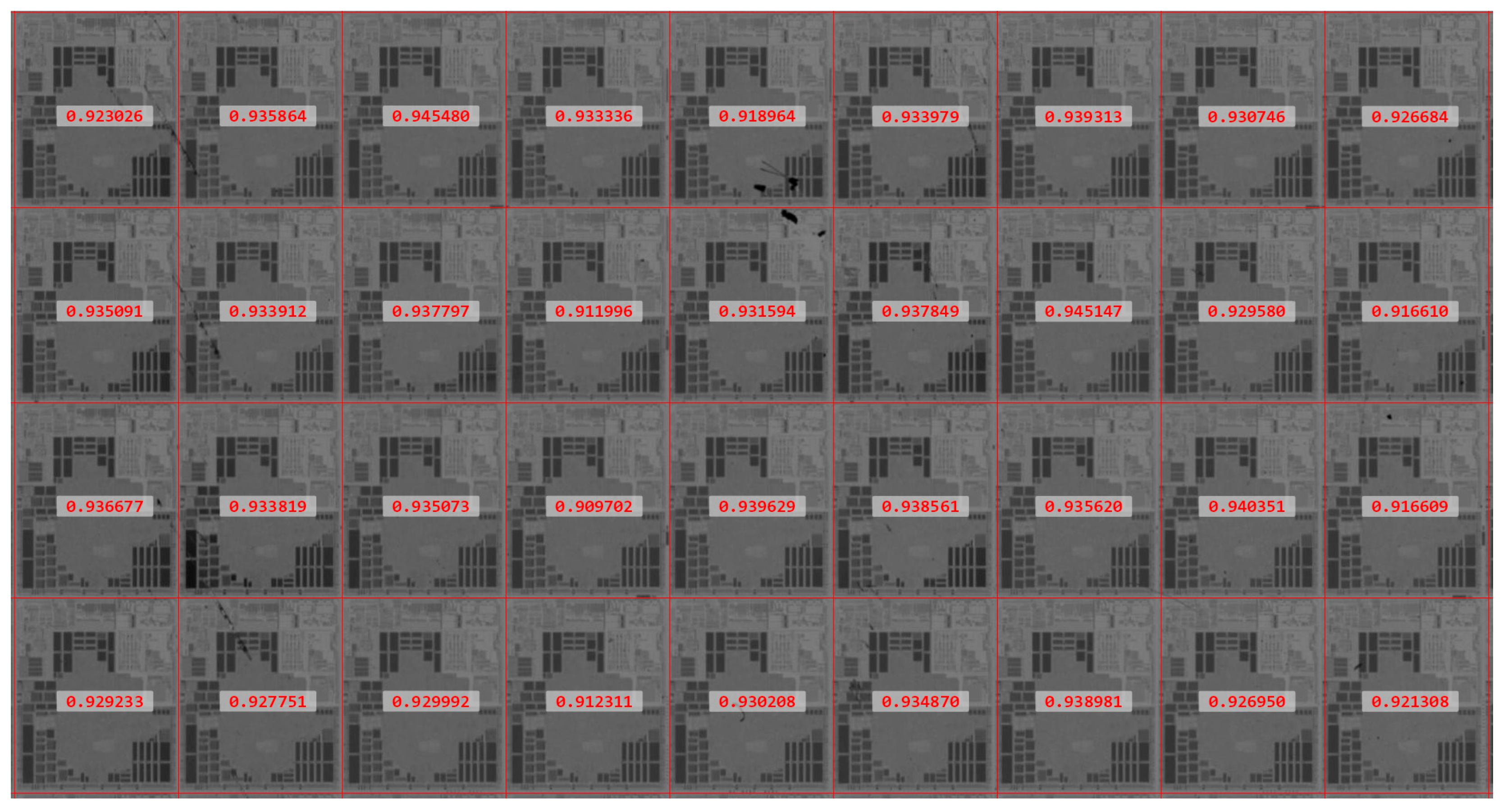
2.2.1. Period Measurement
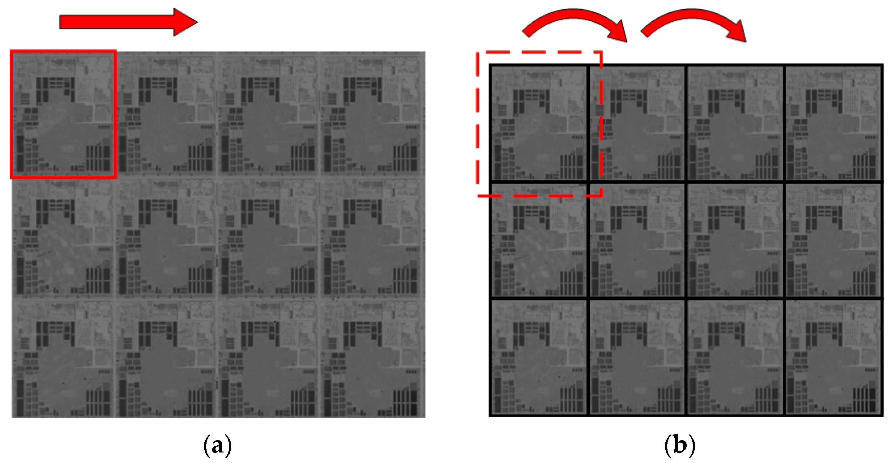
2.2.2. Reconstruction of Background Image
2.2.3. Image Difference
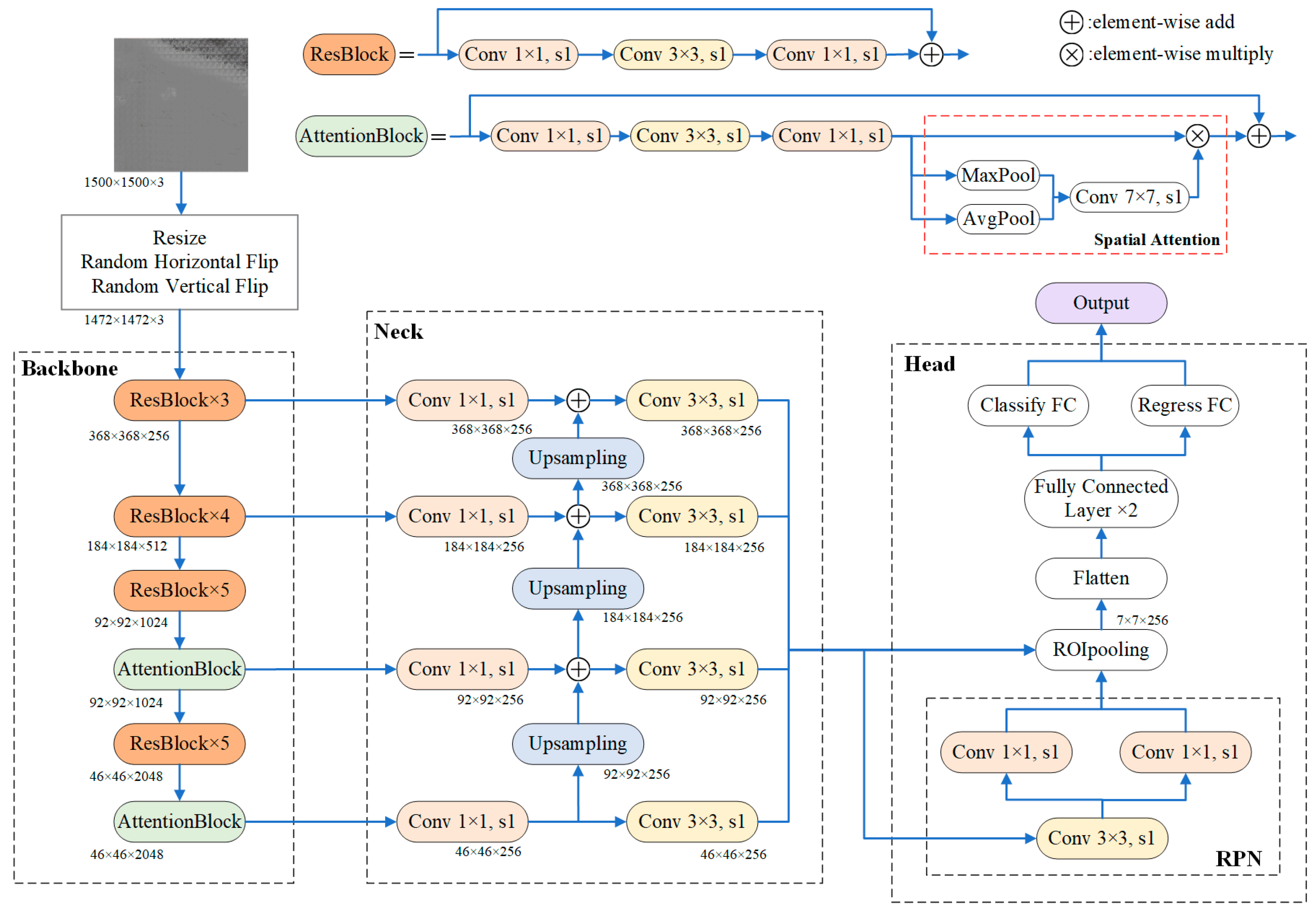
2.3. Faster R-CNN Network
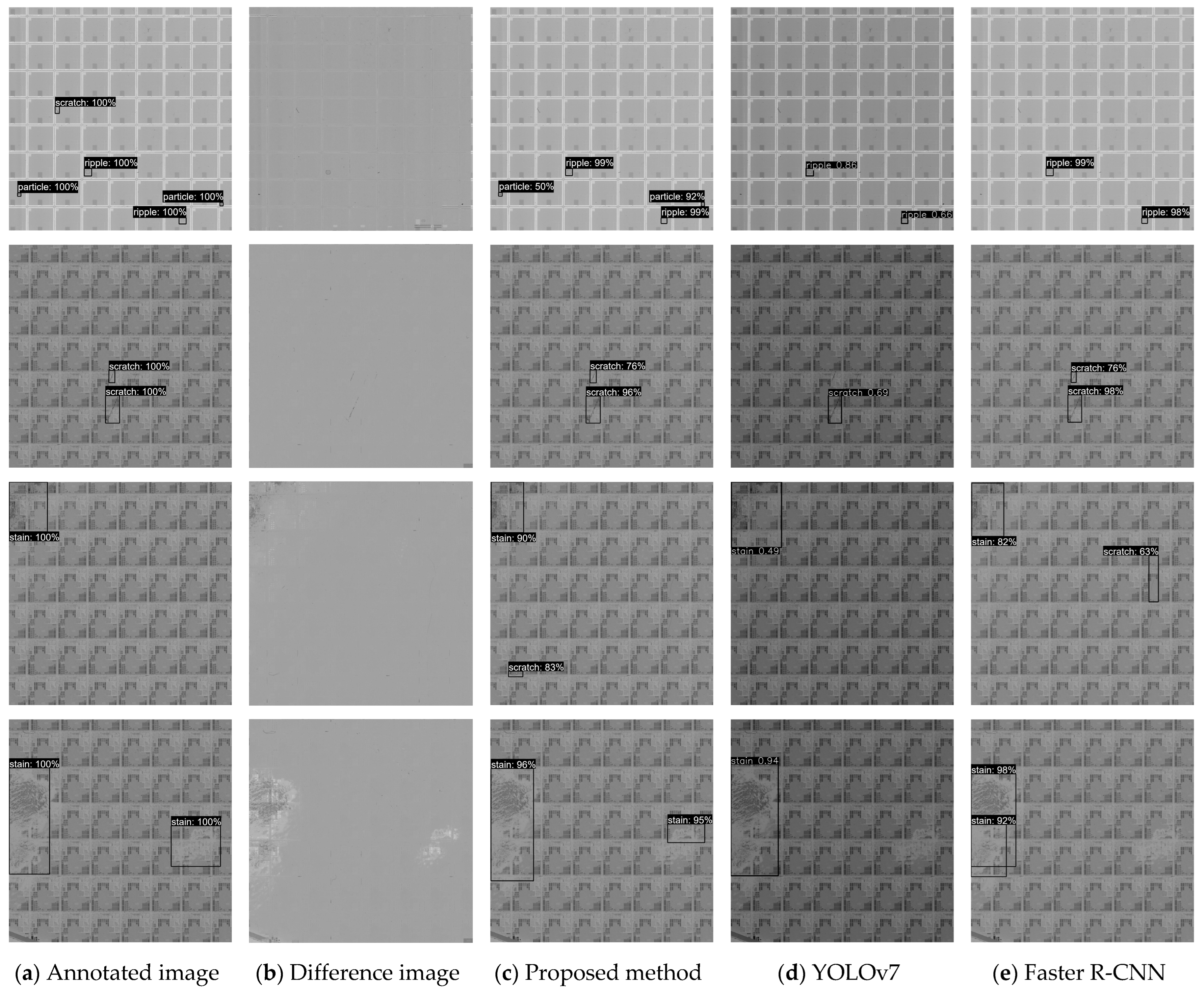
3. Experimental Results and Analysis
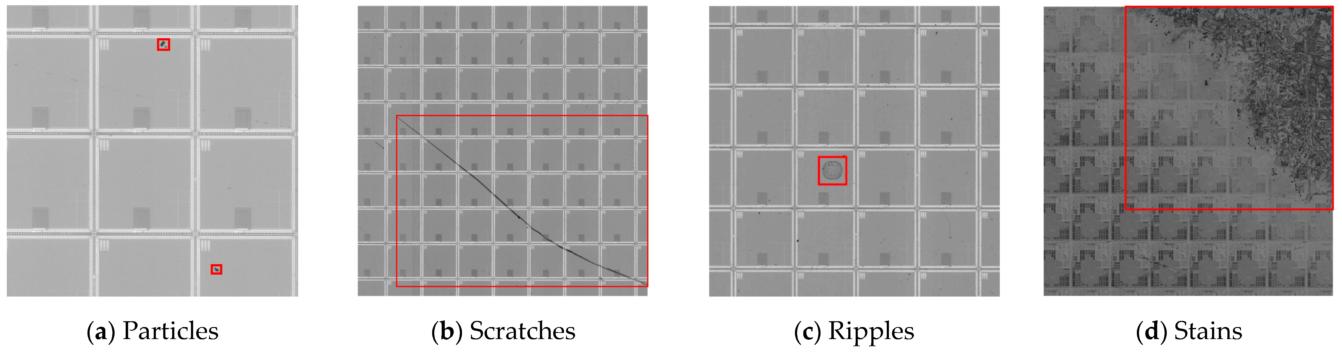
3.1. Experimental Environment and Dataset
3.2. Detection Results
3.3. Ablation Study
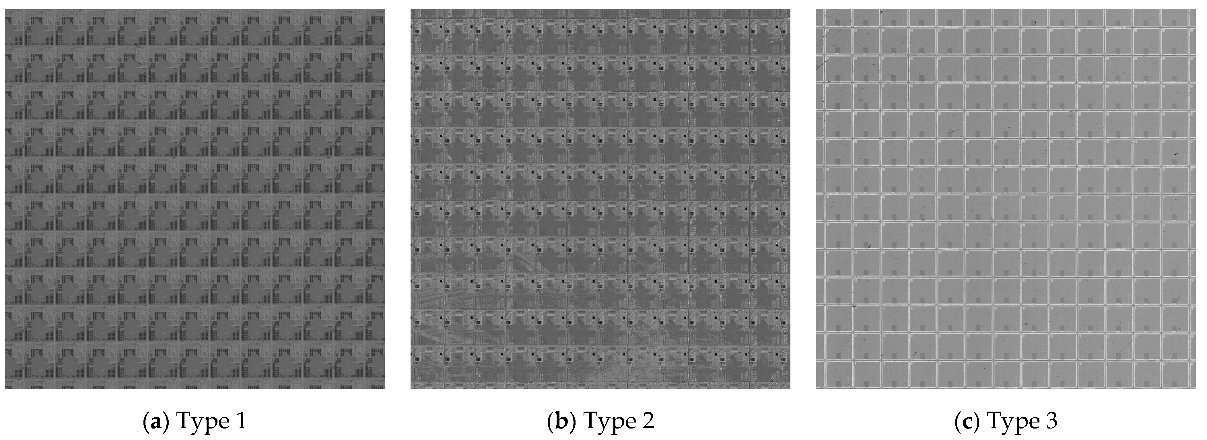
3.4. Effectiveness Analysis of the Period Measurement Algorithm
3.5. Performance Analysis of Training Dataset
4. Conclusions
Author Contributions
Funding
Institutional Review Board Statement
Informed Consent Statement
Data Availability Statement
Conflicts of Interest
References
- Kim, T.S.; Lee, J.W.; Lee, W.K.; Sohn, S.Y. Novel method for detection of mixed-type defect patterns in wafer maps based on a single shot detector algorithm. J. Intell. Manuf. 2022, 33, 1715–1724. [Google Scholar] [CrossRef]
- Hafer, R.; Patterson, O.; Hahn, R.; Xiao, H. Full-wafer voltage contrast inspection for detection of BEOL defects. IEEE Trans. Semicond. Manuf. 2015, 28, 461–468. [Google Scholar] [CrossRef]
- Jizat, J.; Majeed, A.; Nasir, A.; Taha, Z.; Yuen, E. Evaluation of the machine learning classifier in wafer defects classification. ICT Express 2021, 7, 535–539. [Google Scholar] [CrossRef]
- Kang, S. Joint modeling of classification and regression for improving faulty wafer detection in semiconductor manufacturing. J. Intell. Manuf. 2020, 31, 319–326. [Google Scholar] [CrossRef]
- Yang, J.; Xu, Y.; Rong, H.; Du, S.; Zhang, H. A method for wafer defect detection using spatial feature points guided affine iterative closest point algorithm. IEEE Access 2020, 8, 79056–79068. [Google Scholar] [CrossRef]
- Wang, J.; Yu, Z.; Duan, Z.; Lu, G. A sub-region one-to-one mapping (SOM) detection algorithm for glass passivation parts wafer surface low-contrast texture defects. Multimed. Tools Appl. 2021, 19, 28879–28896. [Google Scholar] [CrossRef]
- Li, K.; Liao, P.; Cheng, K.; Chen, L.; Wang, S.; Huang, A.; Chou, L.; Han, G.; Chen, J.; Liang, H.; et al. Hidden wafer scratch defects projection for diagnosis and quality enhancement. IEEE Trans. Semicond. Manuf. 2021, 34, 9–15. [Google Scholar] [CrossRef]
- Gómez-Sirvent, J.; Rose, F.; Sanchez-Reolid, R.; Fernandez-Caballero, A.; Morales, R. Optimal feature selection for defect classification in semiconductor wafers. IEEE Trans. Semicond. Manuf. 2022, 35, 324–330. [Google Scholar] [CrossRef]
- Frittoli, L.; Carrera, D.; Rossi, B.; Fragneto, P.; Boracchi, G. Deep open-set recognition for silicon wafer production monitoring. Pattern Recognit. 2022, 124, 108488. [Google Scholar] [CrossRef]
- Yang, Y.; Sun, M. Semiconductor defect detection by hybrid classical-quantum deep learning. In Proceedings of the IEEE Conference on Computer Vision and Pattern Recognition, New Orleans, LA, USA, 21–24 June 2022; pp. 2313–2322. [Google Scholar]
- Huang, H.; Tang, X.; Wen, F.; Jin, X. Small object detection method with shallow feature fusion network for chip surface defect detection. Sci. Rep. 2022, 12, 3914. [Google Scholar] [CrossRef] [PubMed]
- Wang, S.; Wang, H.; Yang, F.; Liu, F.; Zeng, L. Attention-based deep learning for chip-surface-defect detection. Int. J. Adv. Manuf. Technol. 2022, 121, 1957–1971. [Google Scholar] [CrossRef]
- Wang, X.; Jia, X.; Jiang, C.; Jiang, S. A wafer surface defect detection method built on generic object detection network. Digital Signal Process. 2022, 130, 103718. [Google Scholar] [CrossRef]
- Ren, S.; He, K.; Girshick, R.; Jian, S. Faster R-CNN: Towards real-time object detection with region proposal networks. IEEE Trans. Pattern Anal. Mach. Intell. 2017, 39, 1137–1149. [Google Scholar] [CrossRef] [PubMed]
- Haddad, B.; Dodge, S.; Karam, L.; Patel, N.; Braun, M. Locally adaptive statistical background modeling with deep learning-based false positive rejection for defect detection in semiconductor units. IEEE Trans. Semicond. Manuf. 2020, 33, 357–372. [Google Scholar] [CrossRef]
- Han, H.; Gao, C.; Zhao, Y.; Liao, S.; Tang, L.; Li, X. Polycrystalline silicon wafer defect segmentation based on deep convolutional neural networks. Pattern Recognit. Lett. 2020, 130, 234–241. [Google Scholar] [CrossRef]
- Kim, J.; Nam, Y.; Kang, M.; Kim, K.; Hong, J.; Lee, S.; Kim, D. Adversarial defect detection in semiconductor manufacturing process. IEEE Trans. Semicond. Manuf. 2021, 34, 365–371. [Google Scholar] [CrossRef]
- Woo, S.; Park, J.; Lee, J.; Kweon, I. CBAM: Convolutional block attention module. In Proceedings of the European Conference on Computer Vision, Munich, Germany, 8–14 September 2018; pp. 3–19. [Google Scholar]
- Lin, T.; Dollar, P.; Girshick, R.; He, K.; Hariharan, B.; Belongie, S. Feature pyramid networks for object detection. In Proceedings of the IEEE Conference on Computer Vision and Pattern Recognition, Honolulu, HI, USA, 22–25 July 2017; pp. 936–944. [Google Scholar]
- Tao, Y.; Muthukkumarasamy, V.; Verma, B.; Blumenstein, M. A texture extraction technique using 2D-DFT and Hamming distance. Proceedings of Fifth International Conference on Computational Intelligence and Multimedia Applications, Xi’an, China, 27–30 September 2003. [Google Scholar]
- Epps, J.; Ambikairaja, E.; Akhtar, M. An integer period DFT for biological sequence processing. In Proceedings of the IEEE International Workshop on Genomic Signal Processing and Statistics, Phoenix, AZ, USA, 8–10 June 2008. [Google Scholar]
- Park, K.; Hong, J.; Kim, W. A methodology combining cosine similarity with classifier for text classification. Appl. Artif. Intell. 2020, 34, 396–411. [Google Scholar] [CrossRef]
- He, K.; Zhang, X.; Ren, S.; Sun, J. Deep residual learning for image recognition. In Proceedings of the IEEE Conference on Computer Vision and Pattern Recognition, Las Vegas, NV, USA, 26–30 June 2016; pp. 770–778. [Google Scholar]
- Lin, T.; Goyal, P.; Girshick, R.; He, K.; Dollar, P. Focal loss for dense object detection. IEEE Trans. Pattern Anal. Mach. Intell. 2017, 99, 2999–3007. [Google Scholar]
- Sun, P.; Zhang, R.; Jiang, Y.; Kong, T.; Xu, C.; Zhan, W.; Tomizuka, M.; Li, L.; Yuan, Z.; Wang, C.; et al. Sparse R-CNN: End-to-end object detection with learnable proposals. In Proceedings of the IEEE Conference on Computer Vision and Pattern Recognition, Virtual, 19–25 June 2021; pp. 14449–14458. [Google Scholar]
- Wang, C.; Bochkovskiy, A.; Liao, H. YOLOv7: Trainable bag-of-freebies sets new state-of-the-art for real-time object detectors. arXiv 2022, arXiv:2207.02696. [Google Scholar]


| Particles | Scratches | Ripples | Stains | |
|---|---|---|---|---|
| Training Dataset | 284 | 323 | 196 | 164 |
| Test Dataset | 64 | 67 | 47 | 34 |
| Model | Backbone Network | AP/% | mAP/% | |||
|---|---|---|---|---|---|---|
| Particles | Scratches | Ripples | Stains | |||
| RetinaNet | ResNet50 | 76.6 | 63.8 | 79.3 | 70.9 | 72.7 |
| Faster R-CNN | ResNet50 | 81.0 | 68.8 | 84.6 | 75.5 | 77.5 |
| Sparse R-CNN | ResNet50 | 79.6 | 66.1 | 79.2 | 73.2 | 74.5 |
| YOLOv7 | CBS + ELAN | 73.4 | 67.3 | 85.2 | 73.9 | 74.9 |
| Proposed Method | ResNet50 + Attention | 85.7 | 75.3 | 92.2 | 77.7 | 82.7 |
| Model | Background Subtraction | Spatial Attention | AP/% | mAP/% | |||
|---|---|---|---|---|---|---|---|
| Particles | Scratches | Ripples | Stains | ||||
| Faster R-CNN | 81.0 | 68.8 | 84.6 | 75.5 | 77.5 | ||
| √ | 83.9 | 71.3 | 89.2 | 76.2 | 80.2 | ||
| √ | 81.5 | 70.0 | 88.0 | 77.3 | 79.2 | ||
| √ | √ | 85.7 | 75.3 | 92.2 | 77.7 | 82.7 | |
| Texture Type | Manual Measurement | Spectral Analysis | Autocorrelation | Proposed Method |
|---|---|---|---|---|
| Type 1 | 204 | 204.5 | 208.0 | 203.6 |
| 243 | 243.6 | 218.0 | 242.6 | |
| Type 2 | 200 | 200.5 | 200.0 | 200.0 |
| 240 | 239.1 | 159.7 | 239.3 | |
| Type 3 | 185 | 373.5 | 184.7 | 184.5 |
| 183 | 182.8 | 184.0 | 182.8 |
| Model | Numbers of Training Data | AP/% | mAP/% | ||||||
|---|---|---|---|---|---|---|---|---|---|
| Particles | Scratches | Ripples | Stains | Particles | Scratches | Ripples | Stains | ||
| Proposed Method | 284 | 323 | 196 | 164 | 85.7 | 75.3 | 92.2 | 77.7 | 82.7 |
| 253 | 287 | 169 | 140 | 85.2 | 63.5 | 86.2 | 67.6 | 75.6 | |
| 221 | 249 | 146 | 118 | 84.5 | 58.4 | 88.5 | 70.6 | 75.5 | |
| 171 | 198 | 118 | 99 | 82.1 | 52.5 | 82.6 | 60.2 | 69.3 | |
| 141 | 163 | 95 | 79 | 82.4 | 46.1 | 82.0 | 62.5 | 68.3 | |
Disclaimer/Publisher’s Note: The statements, opinions and data contained in all publications are solely those of the individual author(s) and contributor(s) and not of MDPI and/or the editor(s). MDPI and/or the editor(s) disclaim responsibility for any injury to people or property resulting from any ideas, methods, instructions or products referred to in the content. |
© 2023 by the authors. Licensee MDPI, Basel, Switzerland. This article is an open access article distributed under the terms and conditions of the Creative Commons Attribution (CC BY) license (https://creativecommons.org/licenses/by/4.0/).
Share and Cite
Zheng, J.; Zhang, T. Wafer Surface Defect Detection Based on Background Subtraction and Faster R-CNN. Micromachines 2023, 14, 905. https://doi.org/10.3390/mi14050905
Zheng J, Zhang T. Wafer Surface Defect Detection Based on Background Subtraction and Faster R-CNN. Micromachines. 2023; 14(5):905. https://doi.org/10.3390/mi14050905
Chicago/Turabian StyleZheng, Jiebing, and Tao Zhang. 2023. "Wafer Surface Defect Detection Based on Background Subtraction and Faster R-CNN" Micromachines 14, no. 5: 905. https://doi.org/10.3390/mi14050905