Article

Low Switching Loss Built-In Diode of High-Voltage RC-IGBT with Shortened P+ Emitter

School of Automation Engineering, University of Electronic Science and Technology of China, Chengdu 611731, China
*
Author to whom correspondence should be addressed.
Micromachines 2023, 14(4), 873; https://doi.org/10.3390/mi14040873
Submission received: 2 March 2023 / Revised: 15 April 2023 / Accepted: 17 April 2023 / Published: 19 April 2023
(This article belongs to the Special Issue Power Semiconductor Devices and Applications)

Abstract

:
In this paper, a low switching loss built-in diode of a high-voltage reverse-conducting insulated gate bipolar transistor (RC-IGBT) is proposed without deteriorating IGBT characteristics. It features a particular shortened P+ emitter (SE) in the diode part of RC-IGBT. Firstly, the shortened P+ emitter in the diode part can suppress the hole injection efficiency resulting in the reduced carriers extracted during the reverse recovery process. The peak of the reverse recovery current and switching loss of the built-in diode during reverse recovery is therefore lowered. Simulation results indicate that the diode’s reverse recovery loss of the proposed RC-IGBT is lowered by 20% compared with that of the conventional RC-IGBT. Secondly, the separate design of the P+ emitter prevents the performance of IGBT from deteriorating. Finally, the wafer process of the proposed RC-IGBT is almost the same as that of conventional RC-IGBT, which makes it a promising candidate for manufacturing.

1. Introduction

To minimize the size of IGBT modules and manufacturing costs meanwhile improving the power conversion efficiency, the reverse-conducting insulated gate bipolar transistor (RC-IGBT) has been proposed [1,2,3]. An IGBT and a freewheeling diode are integrated into one chip which enables RC-IGBT both during forward and reverse conduction [4,5,6,7]. Due to the advantages above, RC-IGBT is a promising device in the power semiconductor field. However, RC-IGBT also suffers from some inherent defects. The snap-back occurring in the forward conduction state is a well-known problem [8,9]. Furthermore, RC-IGBT has complex trade-off relationships between IGBT characteristics, IGBT’s on-state forward voltage drop (VCE(sat)) and the turn-off energy loss (Eoff), and built-in diode characteristics, diode’s forward voltage drop (Von,diode) and the diode’s reverse recovery loss (Err). Therefore, it is difficult to obtain a well-balanced performance between IGBT and a built-in diode. The Err is the main proportion of switching energy loss for RC-IGBT. Lifetime control techniques [10,11] are widely used for a diode in the case of a high-frequency operation. However, the heavy lifetime control realizing the low diode switching energy loss will severely sacrifice the IGBT’s performance.
There are many efforts to solve this problem [12,13]. In recent years, a new contact structure of RC-IGBT is also proposed to lower the diode switching loss by reducing the injection efficiency [2]. In summary, there are two methods to improve the trade-off relationship between Von,diode and Err for RC-IGBT. One is changing the carrier lifetime in Si bulk by the electron beam or proton irradiation to control the carrier transport efficiency; the other is changing the anode or cathode structure to control the carrier injection efficiency.
In this paper, a low Err diode of RC-IGBT with a particular shortened P+ emitter (SE RC-IGBT) is proposed, which is almost not changing the wafer process of the conventional RC-IGBT. The peak of reverse recovery current density (JPR) and switching loss of the built-in diode during reverse recovery are reduced by shortening the length of the P+ emitter in the diode part. Simulation results show that the JPR is lowered by 17.7%, from 16.6 A/cm2 to 14.1 A/cm2, while the IGBT characteristics are maintained.

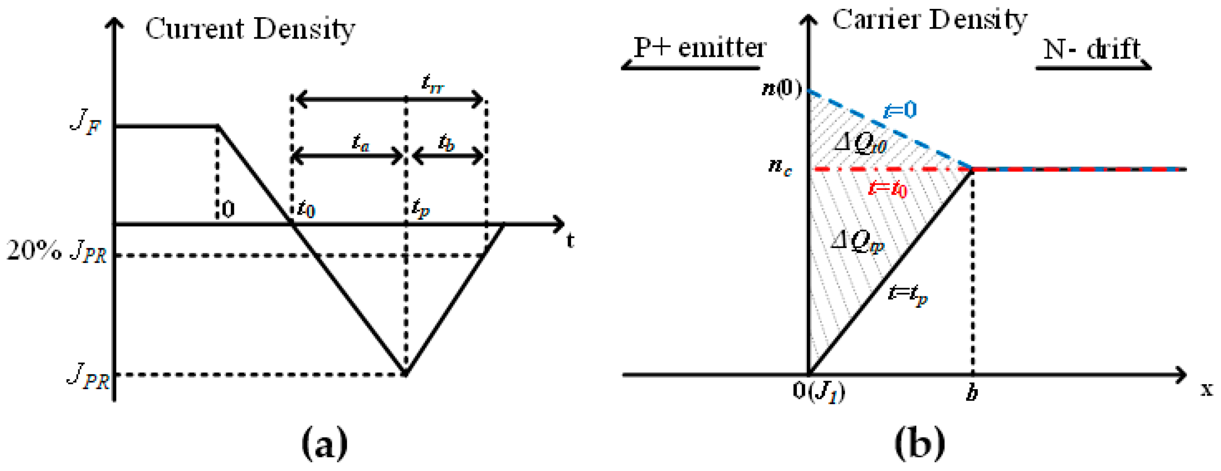
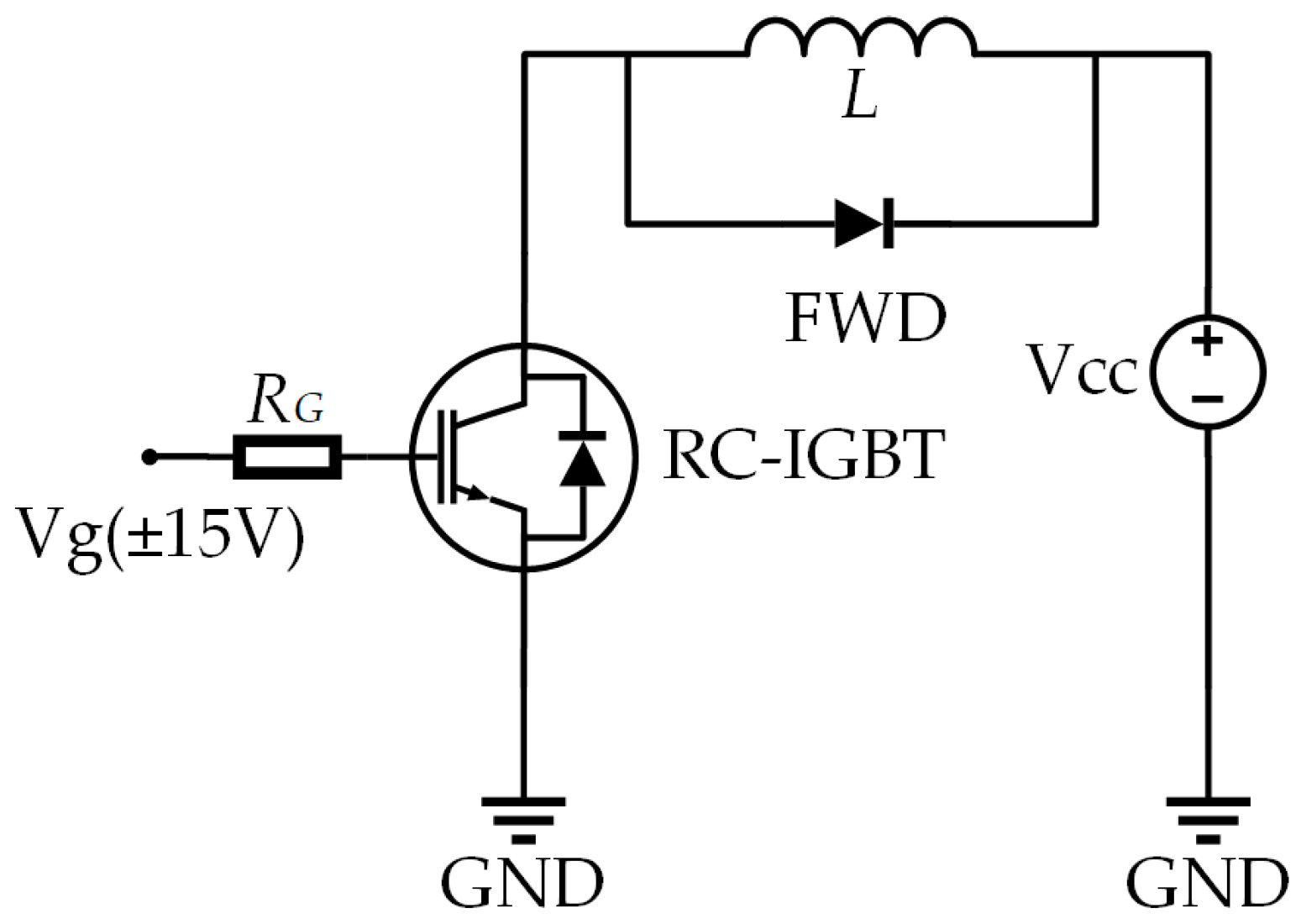
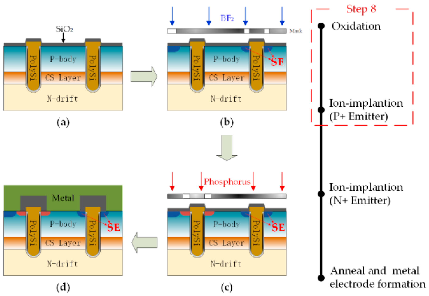
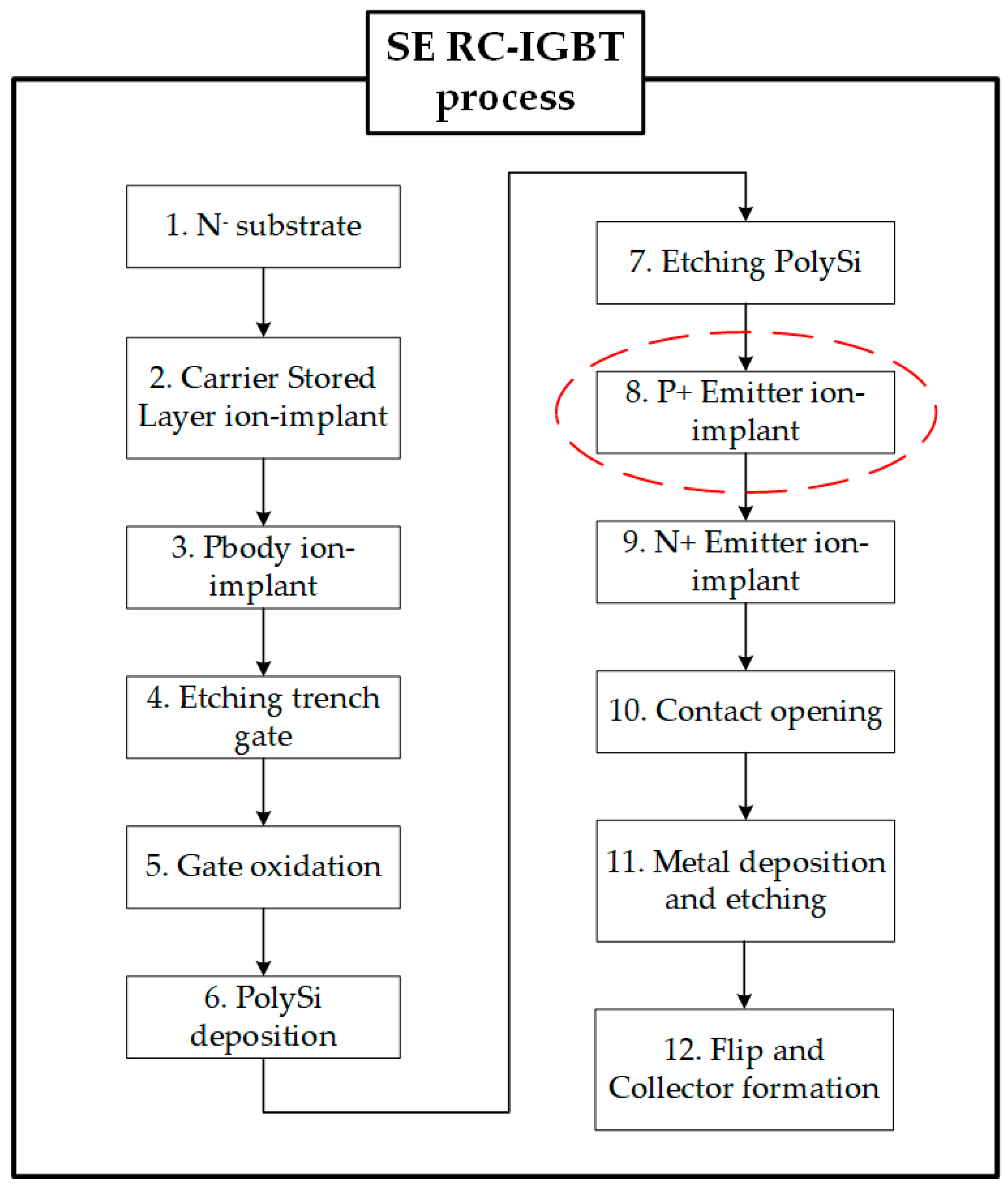
2. Device Structure and Mechanism

Figure 1 shows the cross-sections of conventional RC-IGBT (Con. RC-IGBT) and SE RC-IGBT. There is a carrier stored (CS) layer below the P-base to reduce VCE(sat). The dummy trenches used to reduce the electric field in the carrier stored layer increase the breakdown voltage. Comparing with the Con. RC-IGBT, the proposed SE RC-IGBT features particularly shortened P+ emitters, which are set beside the dummy trench. Further, the P+ emitters between regular trench gates are the same as the Con. RC-IGBT’s.
The turn-off current density characteristics and an approximate representation of carrier distribution at different time intervals during the reverse recovery of the built-in diode are shown in Figure 2a,b, respectively. The JPR is the reverse peak recovery current density at time tp illustrated in Figure 2a, when the built-in diode begins to support the reverse voltage. At this time, the carrier density at J1 junction becomes zero, as illustrated in Figure 2b. The switching time trr is defined as the time interval between t0 and the time when the reverse recovery current has decayed down to 20% of JPR. The subdivision of trr in ta and tb is shown in Figure 2a. It is assumed that the carrier density decreases at J1 junction while remaining relatively constant nc within the N-drift region at a distance b.
Under high-level injection, the on-state current density (JF) at t = 0 can be written as [14],
J F = 1 2 q D P d n ( x ) d x | x = 0
where Dp is the bipolar diffusion constant, q is the charge constant. It can be obtained from Figure 2b,
d n ( x ) d x | x = 0 = n c n ( 0 ) b
Substituting Equation (2) into Equation (1), b can be given by,
b = 2 q D P [ n ( 0 ) n c ] J F
Under the assumption that the carrier density varies linearly over the distance b from 0 to nc, the JPR at time tp is given by,
J P R = 2 q D P n c b
Making the assumption that the on-state current density is determined by recombination, the JF can also be expressed as follow,
J F = Q τ H L = q n c W τ H L
where Q is the stored charge in the N-drift region due to the on-state current flow, τHL is the high-level lifetime in the N-drift region, and W is the length of the N-drift region.
Substituting Equation (5) into Equation (4)
J P R = τ H L J F 2 q W [ n c n ( 0 ) ]
The n(0) is given by [14]
n ( 0 ) = p ( 0 ) = N A exp ( q V 2 k 0 T )
where V is the voltage drop at J1 junction, k0T is the temperature constant, NA is the doping concentration of the P-type region in the built-in diode, including the P-base region and the P+ emitter region. Substituting Equation (7) into Equation (6), JPR can be written as
J P R = τ H L J F 2 q W [ n c N A exp ( q V 2 k 0 T ) ]
The NA of SE RC-IGBT decreases by shortening the length of the P+ emitter in the diode part. Further, nc remains due to the JF being unchanged according to Equation (5). Therefore, the JPR of SE RC-IGBT is supposed to be decreased by Equation (8).
Figure 3 shows the hole density distribution when the built-in diode is turn-on which is the same as the electron density distribution due to the principle of electric neutrality. It is seen that the hole density of SE RC-IGBT is evidently lower than that of the Con. RC-IGBT in the drift region closed to the emitter due to a lower carrier injection efficiency of the shortened P+ emitter. Thus, the JPR of SE RC-IGBT must be lower than that of Con. RC-IGBT, according to Equation (6). Reducing JPR is an effective method to lower the diode switching loss [15]. In addition, thanks to the separate design of the P+ emitters in SE RC-IGBT, hole injection efficiency in the IGBT part is not affected, which prevents the IGBT characteristics from deteriorating. Consequently, the proposed SE RC-IGBT can lower the Err without sacrificing IGBT performance and changing the wafer process.

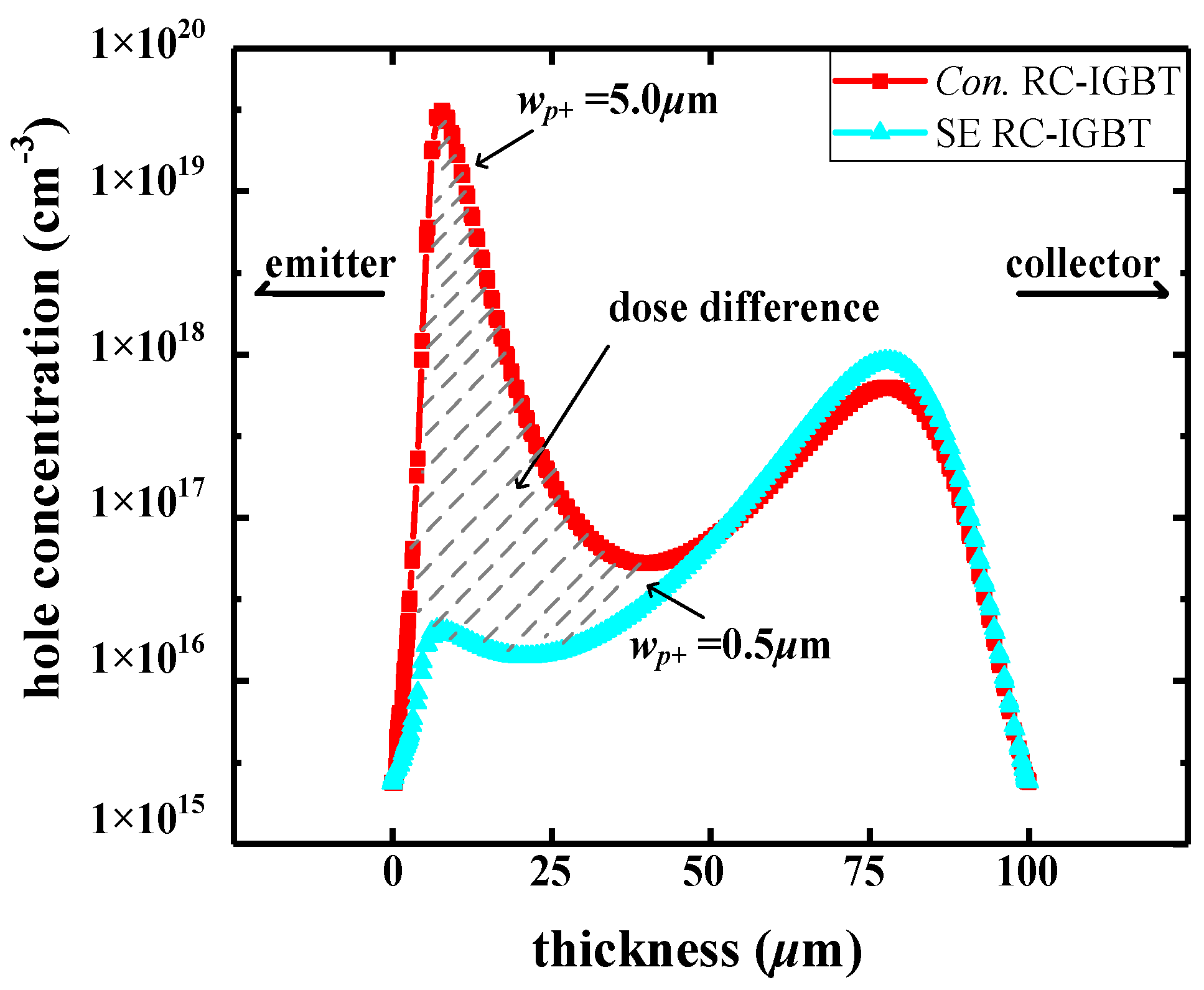
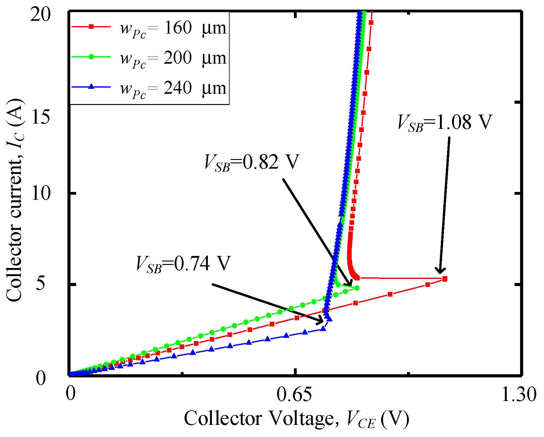
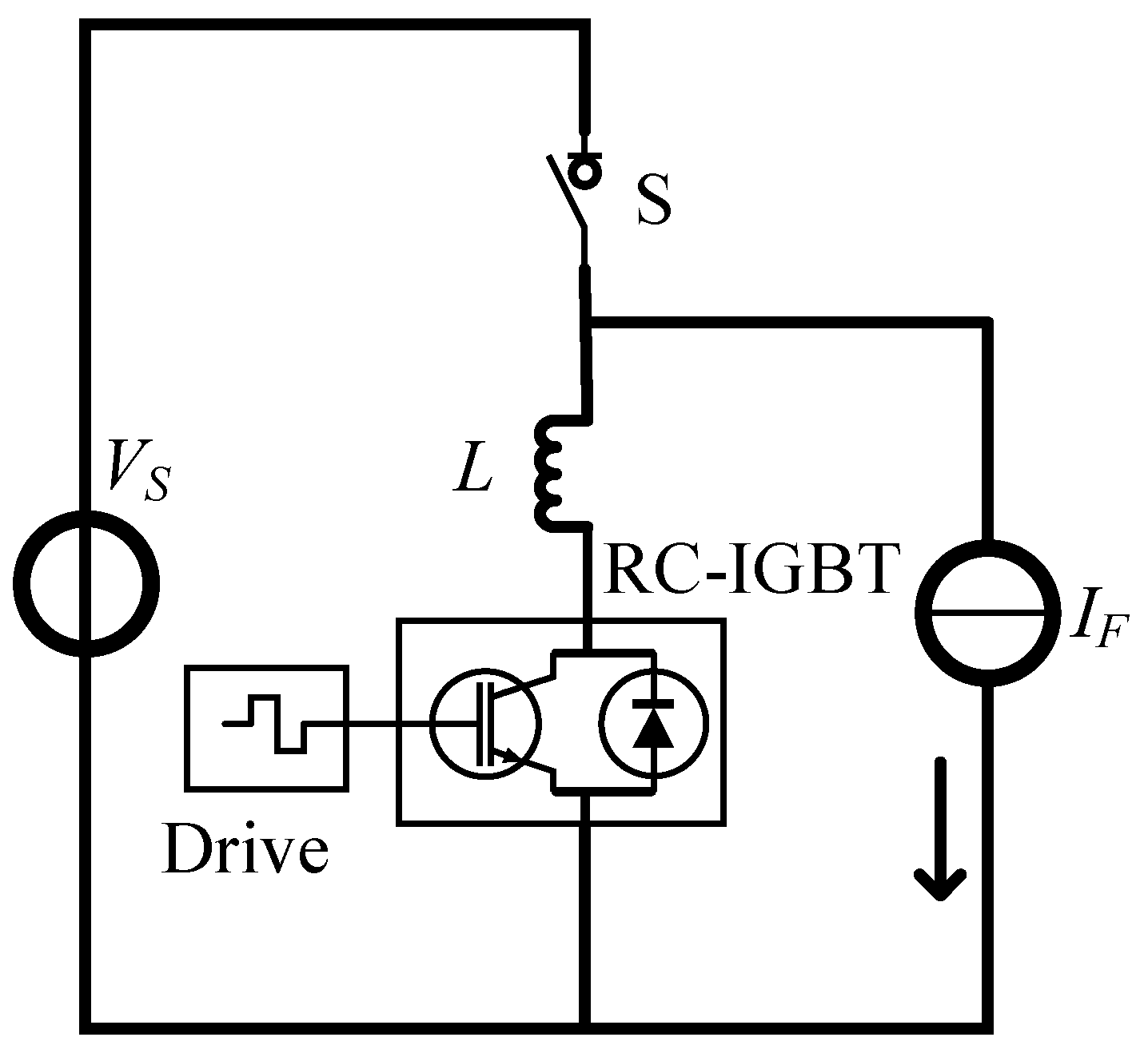
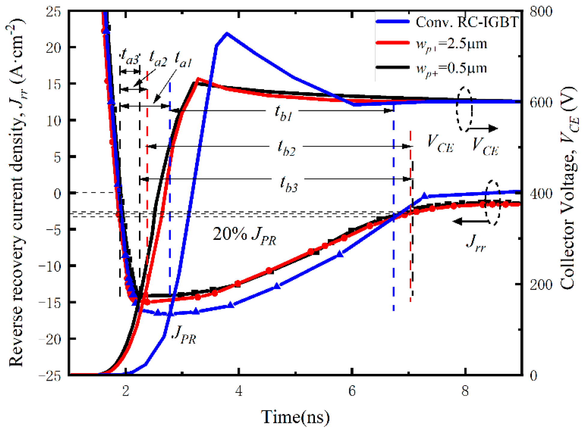
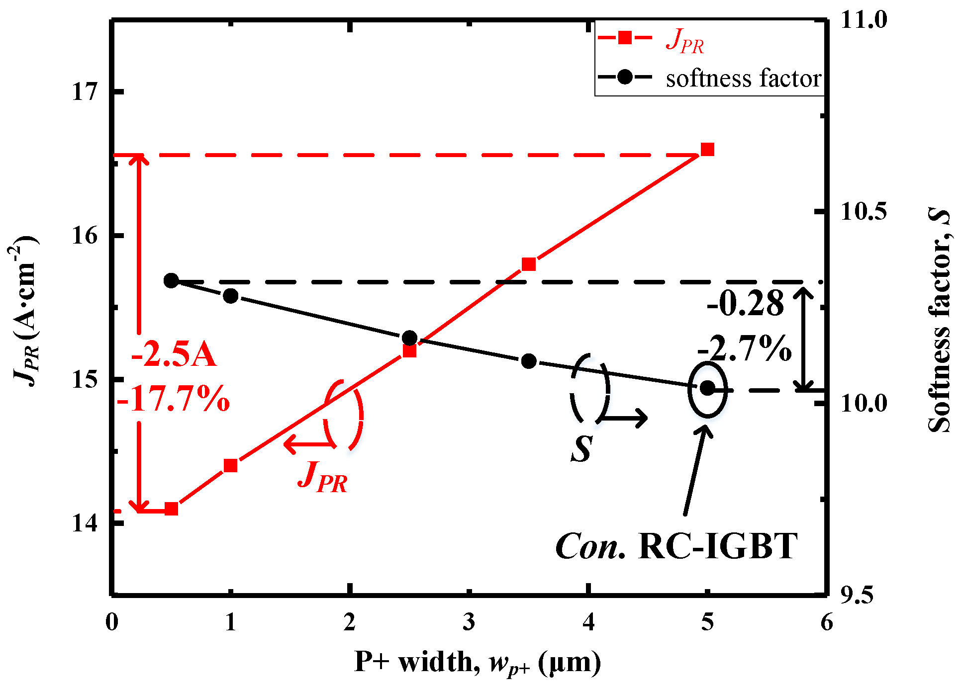
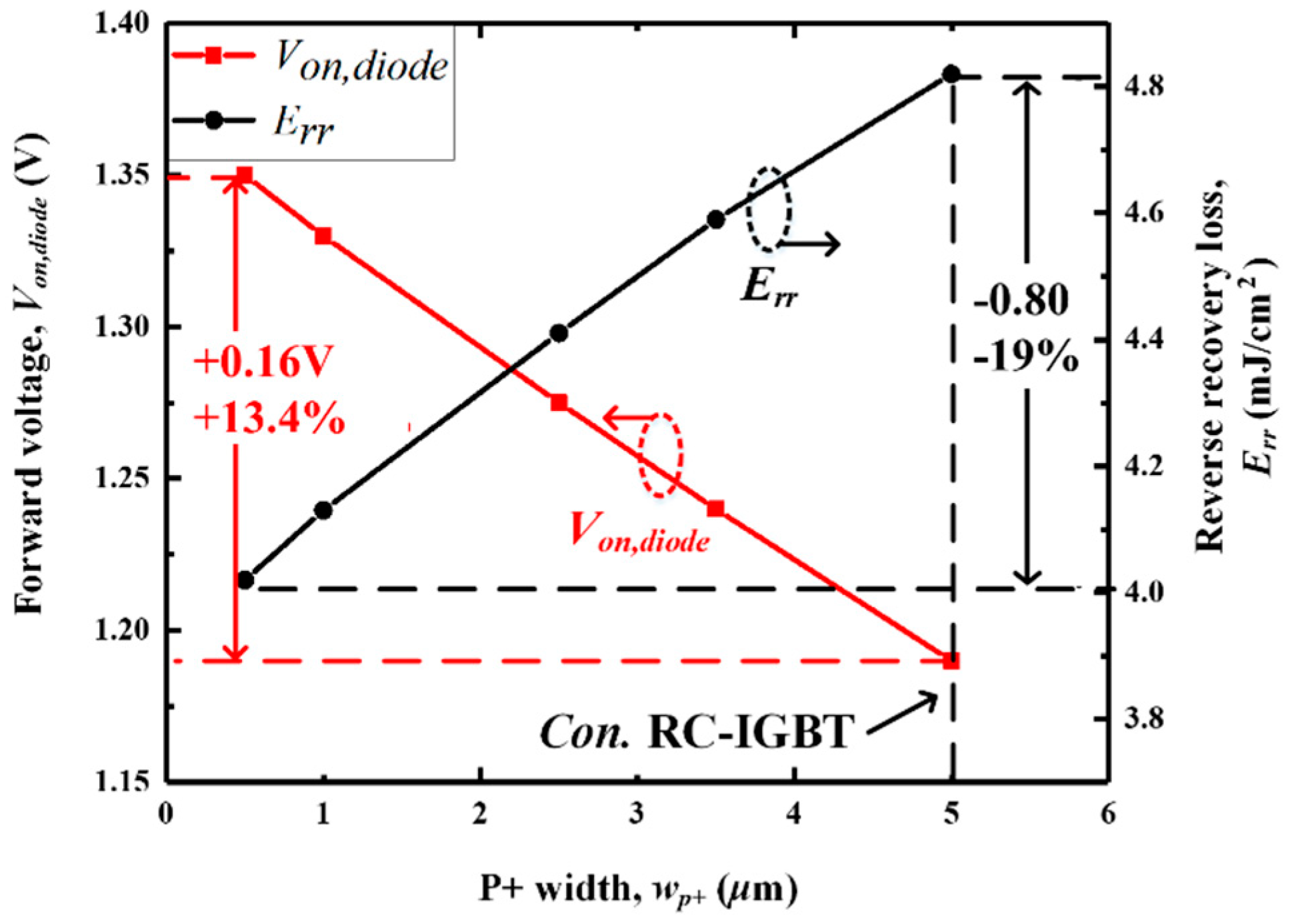
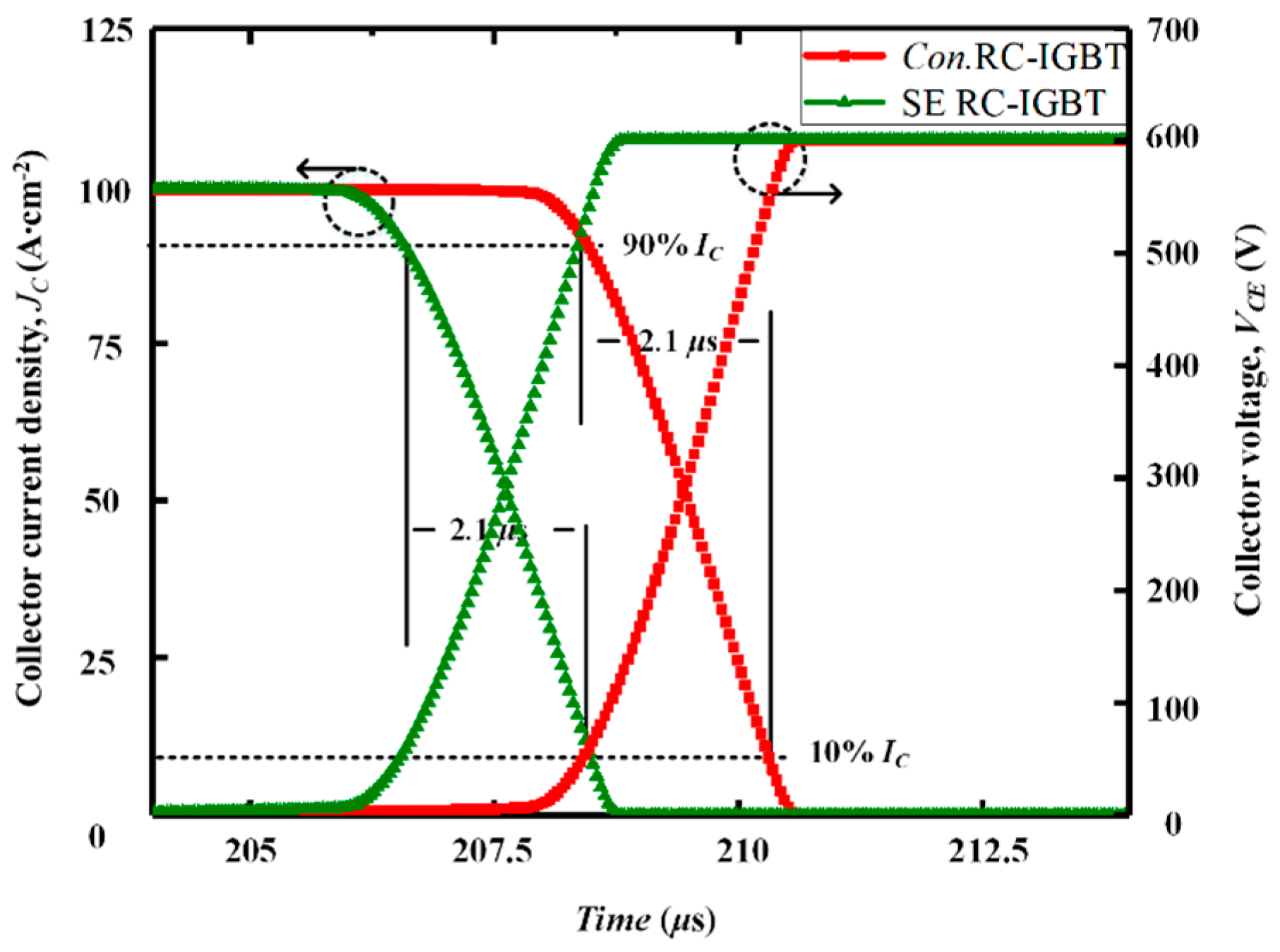
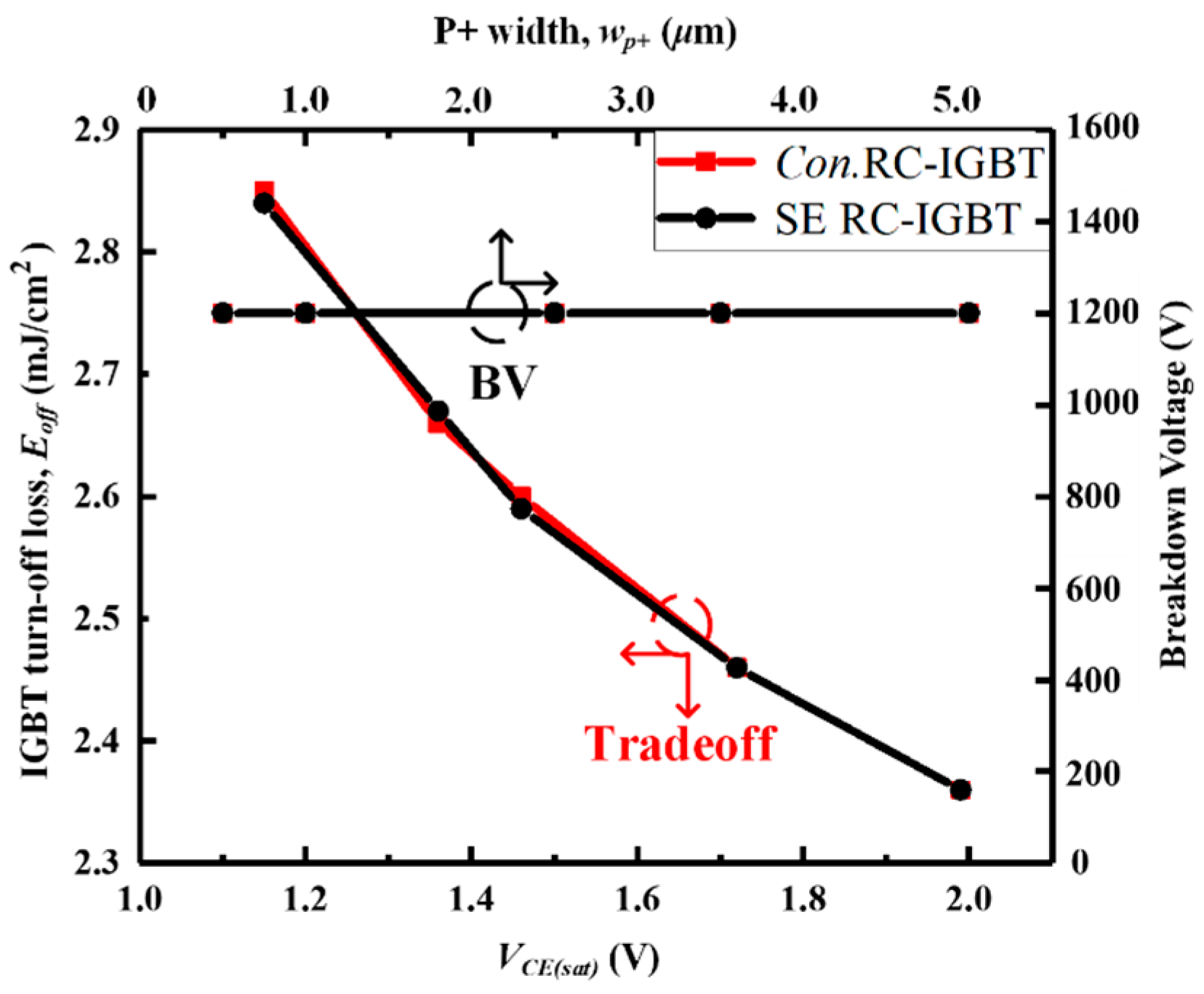
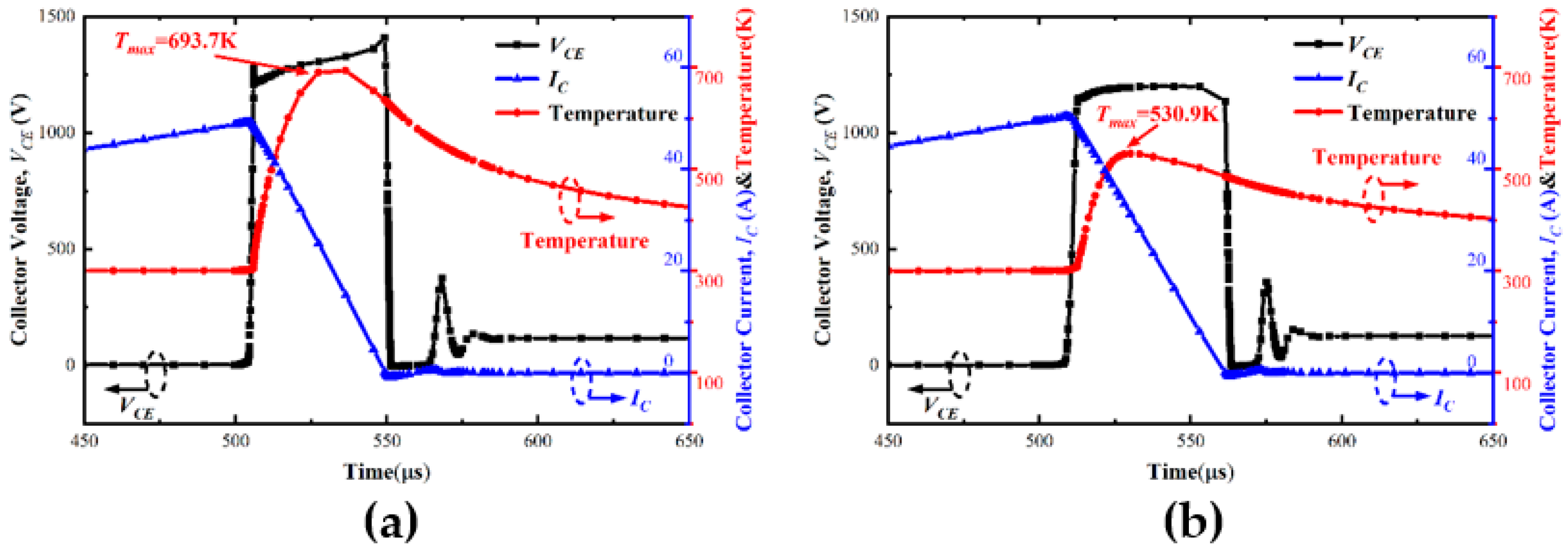
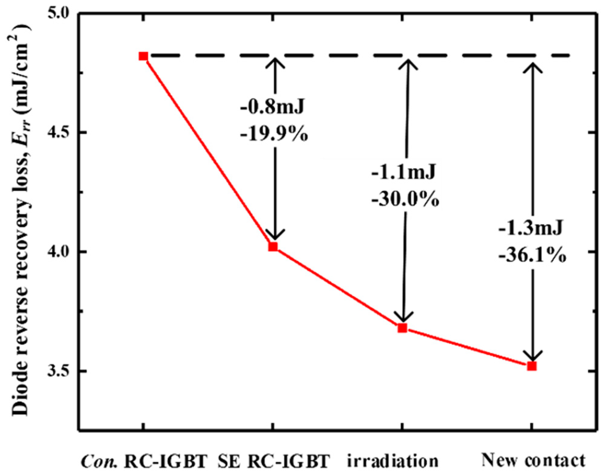
3. Simulation and Discussions

In order to verify the characteristics of the proposed SE RC-IGBT, numerical simulations were performed by TCAD SENTAURUS [16]. A breakdown voltage of 1.2 kV and a threshold voltage of 5 V was designed. The related structure parameters are listed in Table 1. The area of the active region of the SE RC-IGBT is set to 1 cm2.
Figure 4 shows the impact of P-collector width wPc on the snap-back voltage (VSB) of SE RC-IGBT. It can be seen that the snap-back effect was suppressed as the increase in wPc, which was almost eliminated when wPc increased to 240 μm. The length of the P-collector was set to 240 μm. Therefore, the ratio between the length of the P-collector and the length of the N-collector was set to 8:1.
Figure 5 shows the simulated test circuit for investigating the turn-off behavior of the built-in diode with inductive load. The inductance in the main circuit is set to 200 μH. The reverse recovery current density (JRR) waveforms of the built-in diodes for SE RC-IGBT and Con. RC-IGBT is shown in Figure 6. It can be seen that the JPR and the collector voltage overshoot of SE RC-IGBT are obviously lower than those of Con. RC-IGBT during the reverse recovery. Furthermore, there is a positive correlation between the JPR and the width of the P+ emitter wp+.
Figure 7 shows the dependence of the JPR and softness factor S on the width of the P+ emitter wp+. It can be seen that the JPR of SE RC-IGBT is lowering with the decrease in wp+, which is consistent with the derivation of Equation (8). Furthermore, the JPR of SE RC-IGBT is decreased by 17.7% when wp+ = 0.5 μm, from 16.6 A/cm2 to 14.1 A/cm2, compared with that of the conventional RC-IGBT. The softness factor S is defined as follows:
S = t b t a
where tb and ta are mentioned in Figure 2a. The softness factor represents the attenuation rate of the reverse recovery current. The larger S causes the smaller voltage spike, which means a more secure system. It can be seen that the softness factor S is almost unchanged with the decrease in the P+ emitter width.
Figure 8 shows the dependence of on-state voltage (Von,diode) and Err of the built-in diode on the width of the P+ emitter. The Von,diode increases with the decrease in the P+ emitter width due to the suppression of the carrier injection efficiency of the P+ emitter. However, the Err of SE RC-IGBT is decreased by 19% when the P+ emitter width is shortened from 5 μm to 0.5 μm.
Figure 9 shows the inductive load circuit for the switching simulation of RC-IGBT. The inductive load is set to 200 μH. The IGBT turn-off characteristics of Con. RC-IGBT and SE RC-IGBT are shown in Figure 10. It can be seen that the turn-off time of SE RC-IGBT is almost the same as that of the conventional RC-IGBT.
Figure 11 shows the dependences of breakdown voltage (BV) on wp+ and the trade-off relationship between Eoff and VCE(sat) at different P-collector doping concentrations for Con. RC-IGBT and SE RC-IGBT. It is seen that the BV of SE RC-IGBT is the same as that of the conventional RC-IGBT because the IGBT part is unchanged. Furthermore, the trade-off relationship between Eoff and VCE(sat) of SE RC-IGBT is also not deteriorated. As a result, the SE RC-IGBT improves the turn-off characteristics of the built-in diode without deterioration of IGBT performance.
The simulated temperature, collector–emitter voltage, and collector current waveforms of the Conv. RC-IGBT and SE RC-IGBT with a 0.5 ms unclamped inductive switching (UIS) pulse are shown in Figure 12. The on-stage time tON is 0.5 ms to make the avalanche current Iav reach 50 A for both Conv. RC-IGBT and SE RC-IGBT. The maximum collector voltages of SE RC-IGBT were reduced by 14% compared to that of Conv. RC-IGBT from 1409.4 V to 1200.3 V. The avalanche time tav of SE RC-IGBT was increased by 19% compared to that of Conv. RC-IGBT from 46 μs to 55 μs. So the dIav/dt of SE RC-IGBT is 0.9 A∙μs−1, which was reduced by 18% compared to 1.1 A∙μs−1 of Conv. RC-IGBT. Furthermore, the maximum temperature during the UIS transient in SE RC-IGBT reached 530.9 K lower than 693.7 K in the Conv. RC-IGBT, which indicates that the UIS failure in the SE RC-IGBT will be less likely to be triggered by a high-temperature transient.
Figure 13 shows the simple key processing steps to fabricate the front side of the SE RC-IGBT. The backside processing steps are not needed to be addressed in this article. Instead of changing the front-side processing, the modification of the lithographic mask is only required before the P+ emitter ion implant. First, grow oxide to suppress the channeling effect in the ion implantation, as shown in Figure 13a. Next, redefine the lithographic mask and BF2 ion implant, as shown in Figure 13b. Furthermore, N+ collectors are formed by phosphorus ion implantation, as shown in Figure 13c. Then, anneal and form the metal electrode, as shown in Figure 13d. Figure 14 shows the process flow for SE RC-IGBT. The wafer process of SE RC-IGBT is the same as that of Con. RC-IGBT. Only the lithographic mask needs to be redefined at the step of the P+ emitter ion-implant circled by dotted lines.
The Err of different kinds of RC-IGBT are compared in Figure 15. The RC-IGBT with the new contact structure in [2] shows the lowest Err. However, it has a difficult and highly cost manufacturing. Lifetime control by electron beam irradiation in [10] not only changes the built-in diode characteristics but also deteriorates the IGBT performance. Although the SE RC-IGBT proposed in this paper shows an inferior effect of decreasing Err, it does not change the wafer process of conventional RC-IGBT and sacrifice the IGBT characteristics.

4. Conclusions

A particular shortened P+ emitter RC-IGBT (SE RC-IGBT) is proposed and investigated by simulation. The characteristics of IGBT and the built-in diode are both discussed in this paper. Simulation results show that the Err of SE RC-IGBT has been decreased by about 20% compared with that of the conventional RC-IGBT. Furthermore, the soft factor S is almost unchanged. In addition, the SE RC-IGBT process is compatible with the conventional RC-IGBT process, making it a promising candidate for production.

Author Contributions

Conceptualization, M.Y. and W.W.; methodology, Y.L. and M.Y.; software, W.W.; validation, W.W., M.Y., and Y.C.; formal analysis, W.W., Y.L., Y.S. and C.G.; investigation, M.Y. and Y.S.; resources, W.W.; data curation, M.Y.; writing—original draft preparation, M.Y.; writing—review and editing, W.W.; visualization, M.Y. and C.G.; supervision, W.W.; project administration, W.W.; funding acquisition, W.W. All authors have read and agreed to the published version of the manuscript.

Funding

This research was funded by the National Natural Science Foundation of China, grant number 61804025, and the Fundamental Research Funds for the Central Universities, grant number ZYGX2019J061.

Data Availability Statement

Not applicable.

Acknowledgments

Thanks for the support of the Institute of Electric Vehicle Driving System and Safety Technology, UESTC.

Conflicts of Interest

The authors declare no conflict of interest.

References

  1. Findlay, E.M.; Udrea, F. Reverse-Conducting Insulated Gate Bipolar Transistor: A Review of Current Technologies. IEEE Trans. Electron. Devices 2019, 66, 219–231. [Google Scholar] [CrossRef]
  2. Suzuki, K.; Yoshida, T.; Haraguchi, Y.; Koketsu, H.; Narazaki, A. Low Switching Loss Diode of 600V RC-IGBT with New Contact Structure. In Proceedings of the International Symposium on Power Semiconductor Devices and ICs, Nagoya, Japan, 30 May–3 June 2021; pp. 31–34. [Google Scholar] [CrossRef]
  3. Zhang, X.D.; Wang, Y.; Wu, X.; Bao, M.T.; Yu, C.H.; Cao, F. An Improved VCE-EOFFTradeoff and Snapback-Free RC-IGBT with P Pillars. IEEE Trans. Electron. Devices 2020, 67, 2859–2864. [Google Scholar] [CrossRef]
  4. Xu, X.; Chen, Z. Simulation Study of a Novel Full Turn-On RC-IGBT with Ultralow Energy Loss. IEEE Electron. Device Lett. 2019, 40, 757–760. [Google Scholar] [CrossRef]
  5. Chen, Y.; Zhang, P.; Hu, X.; Huang, H.Z.; Lai, P.; He, Z.; Chen, Y.; Fu, Z.W.; Liu, C. Study on Electrothermal Characteristics of the Reverse-Conducting IGBT (RC-IGBT). In Proceedings of the 2020 21st International Conference on Electronic Packaging Technology, ICEPT, Guangzhou, China, 12–15 August 2020. [Google Scholar] [CrossRef]
  6. Nishi, K.; Narazaki, A. CSTBTTM Based Split-Gate RC-IGBT with Low Loss and EMI Noise. In Proceedings of the International Symposium on Power Semiconductor Devices and ICs, Vienna, Austria, 13–18 September 2020; pp. 138–141. [Google Scholar] [CrossRef]
  7. Liu, C.; Wu, G.; Wei, M.; Xu, X.; Xing, P.; Zhang, P.; Sun, R.; Chen, W.; Li, Z.; Zhang, B. A Novel Full Tun-on Reverse-Conducting IGBT with Enhanced Carrier Concentration Modulation in Collector Side. In Proceedings of the 2022 IEEE 16th International Conference on Solid-State and Integrated Circuit Technology, ICSICT, Nangjing, China, 25–28 October 2022. [Google Scholar] [CrossRef]
  8. Rahimo, M.; Reigosa, P.D.; Schulz, N.; Iannuzzo, F. Analysis of the RC-IGBT Snap-Back Phenomenon on the Switching Performance of Parallel Devices. In Proceedings of the International Symposium on Power Semiconductor Devices and ICs, Vienna, Austria, 13–18 September 2020; pp. 482–485. [Google Scholar] [CrossRef]
  9. Diaz Reigosa, P.; Rahimo, M.; Minamisawa, R.; Iannuzzo, F. Switching Stability Analysis of Paralleled RC-IGBTs with Snapback Effect. IEEE Trans. Electron. Devices 2021, 68, 3429–3434. [Google Scholar] [CrossRef]
  10. Nishiwaki, K.; Kushida, T.; Kawahashi, A. A Fast & Soft Recovery Diode with Ultra Small Qrr (USQ-Diode) Using Local Lifetime Control by He Ion Irradiation. In Proceedings of the IEEE International Symposium on Power Semiconductor Devices and ICs (ISPSD), Osaka, Japan, 7 June 2001; pp. 235–238. [Google Scholar] [CrossRef]
  11. Vobecky, J.; Hazdra, P. Future Trends in Local Lifetime Control [Power Semiconductor Devices]. In Proceedings of the 8th International Symposium on Power Semiconductor Devices and ICs, Maui, HI, USA, 23–23 May 1996; pp. 161–164. [Google Scholar] [CrossRef]
  12. Takahashi, K.; Yoshida, S.; Noguchi, S.; Kuribayashi, H.; Nashida, N.; Kobayashi, Y.; Kobayashi, H.; Mochizuki, K.; Ikeda, Y.; Ikawa, O. New Reverse-Conducting IGBT (1200V) with Revolutionary Compact Package. In Proceedings of the International Symposium on Power Semiconductor Devices and ICs, Hiroshima, Japan, 18–21 May 2014; pp. 131–134. [Google Scholar] [CrossRef]
  13. Gejo, R.; Ogura, T.; Misu, S.; Maeda, Y.; Matsuoka, Y.; Yasuhara, N.; Nakamura, K. High Switching Speed Trench Diode for 1200V RC-IGBT Based on the Concept of Schottky Controlled Injection (SC). In Proceedings of the International Symposium on Power Semiconductor Devices and ICs, Prague, Czech Republic, 12–16 June 2016; pp. 155–158. [Google Scholar] [CrossRef]
  14. Baliga, B.J. Fundamentals of Power Semiconductor Devices; Springer: Berlin/Heidelberg, Germany, 2008; pp. 1–1069. [Google Scholar] [CrossRef]
  15. Lutz, J.; Schlangenotto, H.; Scheuermann, U.; de Doncker, R. Semiconductor Power Devices: Physics, Characteristics, Reliability; Springer Nature: Basel, Switzerland, 2011; pp. 1–536. [Google Scholar] [CrossRef]
  16. “SynopsysTCAD”, Synopsys.com, March 2023. Available online: https://www.synopsys.com/silicon/tcad.html (accessed on 16 April 2023).
Figure 1. The cross-section of RC-IGBT. (a) Conventional RC-IGBT; (b) The proposed SE RC-IGBT.
Micromachines 14 00873 g001
Figure 2. The model of the built-in diode. (a) The linearized reverse recovery current density waveform of the built-in diode; (b) The change in carrier distribution at different time intervals during the turn-off process of the built-in diode.
Micromachines 14 00873 g002
Figure 3. Hole density distribution of Conventional RC-IGBT along line AA’ and SE RC-IGBT along line BB’.
Micromachines 14 00873 g003
Figure 4. Impact of the P-collector width wPc on snap-back.
Micromachines 14 00873 g004
Figure 5. Inductive load test circuit for turn-off behavior of built-in diode.
Micromachines 14 00873 g005
Figure 6. Reverse recovery current and collector voltage waveforms of conventional RC-IGBT and SE RC-IGBT. (ta and tb are mentioned in Figure 2a).
Micromachines 14 00873 g006
Figure 7. The change in the JPR and softness factor S with different P+ emitter widths.
Micromachines 14 00873 g007
Figure 8. The change of the Von.,diode and Err with different P+ emitter widths.
Micromachines 14 00873 g008
Figure 9. Inductive load circuit for the switching simulation of RC-IGBT.
Micromachines 14 00873 g009
Figure 10. IGBT turn-off I-V characteristics of conventional RC-IGBT and SE RC-IGBT.
Micromachines 14 00873 g010
Figure 11. Breakdown voltage at different wp+ and trade-off relationship between Eoff and VCE(sat) of conventional RC-IGBT and SE RC-IGBT for different P-collector doping concentrations.
Micromachines 14 00873 g011
Figure 12. The unclamped inductive switching (UIS) waveforms for (a) conventional RC-IGBT and (b) the proposed SE RC-IGBT.
Micromachines 14 00873 g012
Figure 13. Key process steps for fabricating the front side of the SE RC-IGBT. (a) Oxidation; (b) P+ emitter ion implantion; (c) N+ emitter ion implantion; (d) Annealing and metal electrode formation.
Micromachines 14 00873 g013
Figure 14. Process flow for SE RC-IGBT.
Micromachines 14 00873 g014
Figure 15. The built-in diode’s reverse recovery loss Err for several RC-IGBT.
Micromachines 14 00873 g015
Table 1. Device specifications.
Structure ParametersCon. RC-IGBTProposed
P+ width (μm), wp+50.5
P+ doping concentration (cm−3), NAP+1 × 10201 × 1020
P+ thickness (μm), tp+0.20.2
Wafer thickness (μm), tw100100
Cell width (um), wcell270270
P-collector width (μm), wPc240240
Trench pitch (μm), Tp66
Disclaimer/Publisher’s Note: The statements, opinions and data contained in all publications are solely those of the individual author(s) and contributor(s) and not of MDPI and/or the editor(s). MDPI and/or the editor(s) disclaim responsibility for any injury to people or property resulting from any ideas, methods, instructions or products referred to in the content.

