

SET Kinetics of Ag/HfO2-Based Diffusive Memristors under Various Counter-Electrode Materials
 , and
, and
Abstract
: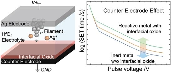
1. Introduction
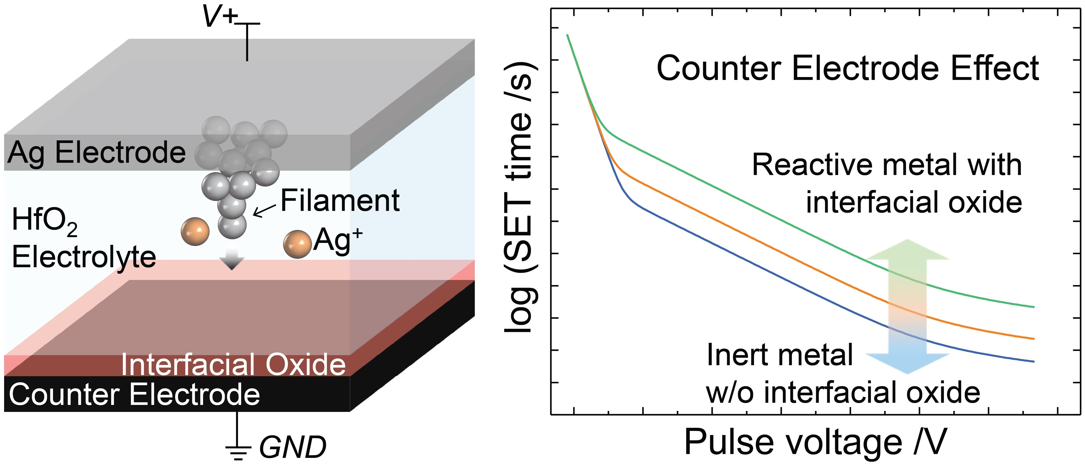
2. Experimental Section
3. Results and Discussion
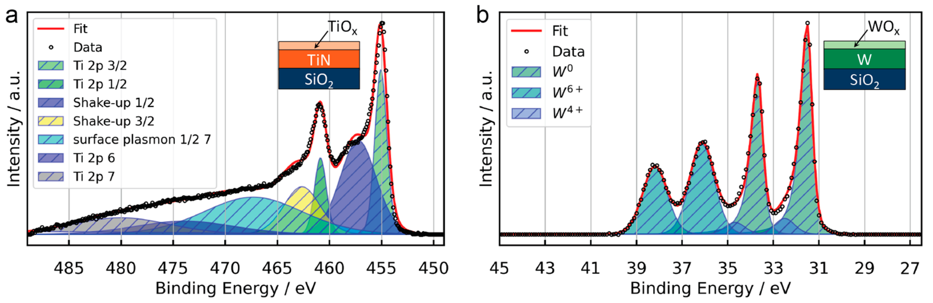
3.1. Surface Oxidation of Counter-Electrode Layer
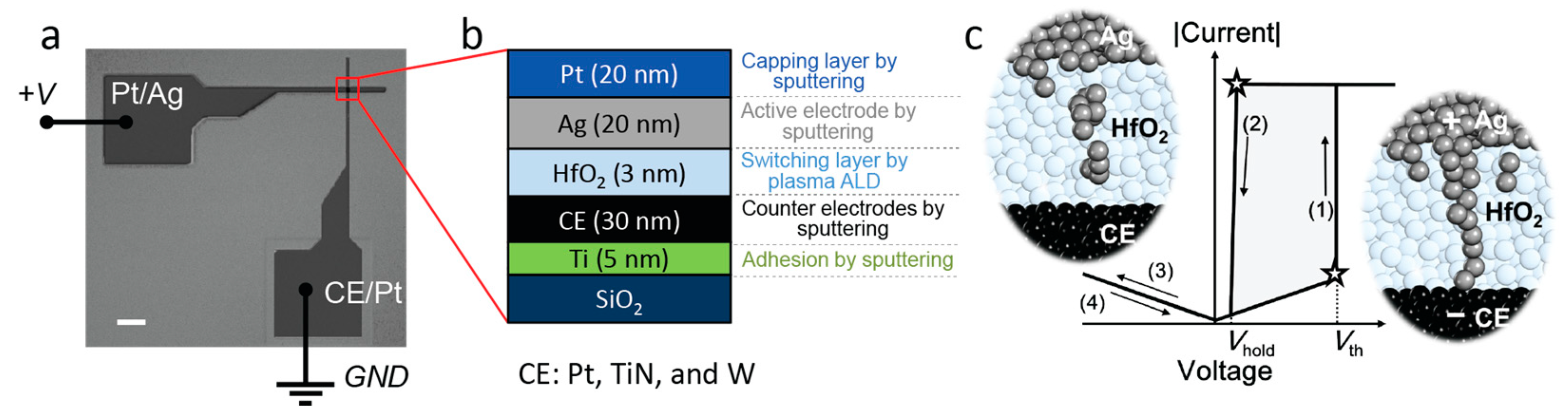
3.2. Forming and Threshold Switching Characteristics
3.3. SET Kinetics
4. Conclusions
Author Contributions
Funding
Data Availability Statement
Acknowledgments
Conflicts of Interest
Appendix A

| Parameter | Off-Axis Sputter | On-Axis Sputter | ||||
|---|---|---|---|---|---|---|
| Ti Adhesion | Pt BE | TiN BE | W BE | Ag AE | Pt Capping | |
| Sputter type | RF | DC | RF | RF | DC | DC |
| Sputter power (W) | 300 | 100 | 100 | 300 | 288 | 359 |
| Ar flow (sccm) | 30 | 30 | 30 | 30 | 60 | 60 |
| Process pressure (mbar) | 0.028 | 0.055 | 0.028 | 0.028 | 1.2 | 2.4 |
| Process temperature (°C) | RT | |||||

References
- Dutta, S.; Detorakis, G.; Khanna, A.; Grisafe, B.; Neftci, E.; Datta, S. Neural Sampling Machine with Stochastic Synapse allows Brain-like Learning and Inference. Nat. Commun. 2022, 13, 2571. [Google Scholar] [CrossRef] [PubMed]
- Zenke, F.; Neftci, E.O. Brain-Inspired Learning on Neuromorphic Substrates. Proc. IEEE 2021, 109, 935–950. [Google Scholar] [CrossRef]
- Wan, W.; Kubendran, R.; Schaefer, C.; Eryilmaz, S.B.; Zhang, W.; Wu, D.; Deiss, S.; Raina, P.; Qian, H.; Gao, B.; et al. A compute-in-memory chip based on resistive random-access memory. Nature 2022, 608, 504–512. [Google Scholar] [CrossRef] [PubMed]
- Dittmann, R.; Menzel, S.; Waser, R. Nanoionic memristive phenomena in metal oxides: The Valence Change Mechanism. Adv. Phys. 2021, 70, 155–349. [Google Scholar] [CrossRef]
- Cheng, B.; Emboras, A.; Salamin, Y.; Ducry, F.; Ma, P.; Fedoryshyn, Y.; Andermatt, S.; Luisier, M.; Leuthold, J. Ultra compact electrochemical metallization cells offering reproducible atomic scale memristive switching. Nat. Commun. Phys. 2019, 2, 28. [Google Scholar] [CrossRef]
- Valov, I.; Lu, W. Nanoscale electrochemistry using dielectric thin films as solid electrolytes. Nanoscale 2016, 8, 13828–13837. [Google Scholar] [CrossRef]
- Sokolov, A.S.; Ali, M.; Riaz, R.; Abbas, Y.; Ko, M.J.; Choi, C. Silver-Adapted Diffusive Memristor Based on Organic Nitrogen-Doped Graphene Oxide Quantum Dots (N-GOQDs) for Artificial Biosynapse Applications. Adv. Funct. Mater. 2019, 29, 1807504. [Google Scholar] [CrossRef]
- Jeon, Y.R.; Abbas, Y.; Sokolov, A.S.; Kim, S.; Ku, B.; Choi, C. Study of in Situ Silver Migration in Amorphous Boron Nitride CBRAM Device. ACS Appl. Mater. Interfaces 2019, 11, 23329–23336. [Google Scholar] [CrossRef]
- Chekol, S.A.; Menzel, S.; Ahmad, R.W.; Waser, R.; Hoffmann-Eifert, S. Effect of the Threshold Kinetics on the Filament Relaxation Behavior of Ag-Based Diffusive Memristors. Adv. Funct. Mater. 2022, 32, 2111242. [Google Scholar] [CrossRef]
- Wang, W.; Covi, E.; Milozzi, A.; Farronato, M.; Ricci, S.; Sbandati, C.; Pedretti, G.; Ielmini, D. Neuromorphic Motion Detection and Orientation Selectivity by Volatile Resistive Switching Memories. Adv. Intell. Syst. 2021, 3, 2000224. [Google Scholar] [CrossRef]
- Rao, M.; Song, W.; Kiani, F.; Asapu, S.; Zhuo, Y.; Midya, R.; Upadhyay, N.; Wu, Q.; Barnell, M.; Lin, P.; et al. Timing Selector: Using Transient Switching Dynamics to Solve the Sneak Path Issue of Crossbar Arrays. Small Sci. 2021, 2, 2100072. [Google Scholar] [CrossRef]
- Chekol, S.A.; Menzel, S.; Waser, R.; Hoffmann-Eifert, S. Strategies to Control the Relaxation Kinetics of Ag-Based Diffusive Memristors and Implications for Device Operation. Adv. Electron. Mater. 2022, 8, 2200549. [Google Scholar] [CrossRef]
- Midya, R.; Wang, Z.; Asapu, S.; Joshi, S.; Li, Y.; Zhuo, Y.; Song, W.; Jiang, H.; Upadhay, N.; Rao, M.; et al. Artificial Neural Network (ANN) to Spiking Neural Network (SNN) Converters Based on Diffusive Memristors. Adv. Electron. Mater. 2019, 5, 1900060. [Google Scholar] [CrossRef]
- Lu, Y.F.; Li, H.-Y.; Li, Y.; Li, L.-H.; Wan, T.-Q.; Yang, L.; Zuo, W.-B.; Xue, K.-H.; Miao, X.-S. A High-Performance Ag/TiN/HfOx/HfOy/HfOx/Pt Diffusive Memristor for Calibration-Free True Random Number Generator. Adv. Electron. Mater. 2022, 8, 2200202. [Google Scholar] [CrossRef]
- Jiang, H.; Belkin, D.; Savel’ev, S.E.; Lin, S.; Wang, Z.; Li, Y.; Joshi, S.; Midya, R.; Li, C.; Rao, M.; et al. A novel true random number generator based on a stochastic diffusive memristor. Nat. Commun. 2017, 8, 882. [Google Scholar]
- Wang, Z.; Joshi, S.; Savel’ev, S.E.; Jiang, H.; Midya, R.; Lin, P.; Hu, M.; Ge, N.; Strachan, J.P.; Li, Z.; et al. Memristors with diffusive dynamics as synaptic emulators for neuromorphic computing. Nat. Mater. 2017, 16, 101–108. [Google Scholar]
- Ilyas, N.; Li, D.; Li, C.; Jiang, X.; Jiang, Y.; Li, W. Analog Switching and Artificial Synaptic Behavior of Ag/SiOx:Ag/TiOx/p(++)-Si Memristor Device. Nanoscale Res. Lett. 2020, 15, 30. [Google Scholar]
- Anwer, S.; Abbas, Y.; Ravaux, F.; Anjum, D.H.; Rezeq, M.; Mohammad, B.; Dongale, T.D.; Liao, K.; Cantwell, W.; Gan, D.; et al. Cobalt oxide nanoparticles embedded in borate matrix: A conduction mode atomic force microscopy approach to induce nano-memristor switching for neuromorphic applications. Appl. Mater. Today 2022, 29, 101691. [Google Scholar] [CrossRef]
- Yang, Y.; Gao, P.; Li, L.; Pan, X.; Tappertzhofen, S.; Choi, S.; Waser, R.; Valov, I.; Lu, W.D. Electrochemical dynamics of nanoscale metallic inclusions in dielectrics. Nat. Commun. 2014, 5, 4232. [Google Scholar]
- Luebben, M.; Menzel, S.; Park, S.G.; Yang, M.; Waser, R.; Valov, I. SET kinetics of electrochemical metallization cells—Influence of counter electrodes in SiO2/Ag based systems. Nanotechnology 2017, 28, 135205. [Google Scholar] [CrossRef]
- Valov, I.; Tsuruoka, T. Effects of moisture and redox reactions in VCM and ECM resistive switching memories. J. Phys. D Appl. Phys. 2018, 51, 413001. [Google Scholar] [CrossRef]
- Russo, U.; Kamalanathan, D.; Ielmini, D.; Lacaita, A.L.; Kozicki, M.N. Study of Multilevel Programming in Programmable Metallization Cell (PMC) Memory. IEEE Trans. Electron Devices 2009, 56, 1040–1047. [Google Scholar] [CrossRef]
- Longnos, F.; Vianello, E.; Cagli, C.; Molas, G.; Souchier, E.; Blaise, P.; Carabasse, C.; Rodriguez, G.; Jousseaume, V.; De Salvo, B.; et al. On the impact of Ag doping on performance and reliability of GeS2-based conductive bridge memories. Solid State Electron. 2013, 84, 155–159. [Google Scholar] [CrossRef]
- Nayak, A.; Tsuruoka, T.; Terabe, K.; Hasegawa, T.; Aono, M. Switching kinetics of a Cu2 S-based gap-type atomic switch. Nanotechnology 2011, 22, 235201. [Google Scholar] [CrossRef]
- Jameson, J.R.; Gilbert, N.; Koushan, F.; Saenz, J.; Wang, J.; Hollmer, S.; Kozicki, M. Effects of cooperative ionic motion on programming kinetics of conductive-bridge memory cells. Appl. Phys. Lett. 2012, 100, 23505. [Google Scholar] [CrossRef]
- Hardtdegen, A.; Zhang, H.; Hoffmann-Eifert, S. Tuning the Performance of Pt/HfO2/Ti/Pt ReRAM Devices obtained from Plasma-Enhanced Atomic Layer Deposition for HfO2 Thin Films. ECS Trans. 2016, 75, 177–184. [Google Scholar] [CrossRef]
- Saha, N.; Tompkins, H. Titanium Nitride Oxidation Chemistry—An X-Ray Photoelectron-Spectroscopy Study. J. Appl. Phys. 1992, 72, 3072–3079. [Google Scholar] [CrossRef]
- You, G.F.; Thong, J.T.L. Thermal oxidation of polycrystalline tungsten nanowire. J. Appl. Phys. 2010, 108, 94312. [Google Scholar] [CrossRef]
- Koroleva, A.A.; Kozodaev, M.G.; Lebedinskii, Y.Y.; Markeev, A.M. Interface engineering for enhancement of the analog properties of W/WO3-(x)/HfO2/Pd resistance switched structures. J. Phys. D Appl. Phys. 2021, 54, 504004. [Google Scholar] [CrossRef]
- Sun, Y.; Zhao, X.; Song, C.; Xu, K.; Xi, Y.; Yin, J.; Wang, Z.; Zhou, X.; Chen, X.; Shi, G.; et al. Performance-Enhancing Selector via Symmetrical Multilayer Design. Adv. Funct. Mater. 2019, 29, 1808376. [Google Scholar] [CrossRef]
- Schindler, C.; Staikov, G.; Waser, R. Electrode kinetics of Cu-SiO2-based resistive switching cells: Overcoming the voltage-time dilemma of electrochemical metallization memories. Appl. Phys. Lett. 2009, 94, 072109. [Google Scholar] [CrossRef]
- Zhuo, Y.; Midya, R.; Song, W.; Wang, Z.; Asapu, S.; Rao, M.; Lin, P.; Jiang, H.; Xia, Q.; Williams, R.S.; et al. A Dynamical Compact Model of Diffusive and Drift Memristors for Neuromorphic Computing. Adv. Electron. Mater. 2021, 8, 2100696. [Google Scholar] [CrossRef]
- Menzel, S.; Tappertzhofen, S.; Waser, R.; Valov, I. Switching Kinetics of Electrochemical Metallization Memory Cells. PCCP 2013, 15, 6945–6952. [Google Scholar] [CrossRef] [PubMed]
- Tappertzhofen, S.; Waser, R.; Valov, I. Impact of Counter Electrode Material on the Redox Processes in Resistive Switching Memories. ChemElectroChem 2014, 1, 1287–1292. [Google Scholar] [CrossRef]
- Arita, M.; Takahashi, A.; Ohno, Y.; Nakane, A.; Tsurumaki-Fukuchi, A.; Takahashi, Y. Switching operation and degradation of resistive random access memory composed of tungsten oxide and copper investigated using in-situ TEM. Sci. Rep. 2015, 5, 17103. [Google Scholar] [CrossRef] [PubMed]
- Song, J.; Woo, J.; Yoo, J.; Chekol, S.A.; Lim, S.; Sung, C.; Hwang, H. Effects of Liner Thickness on the Reliability of AgTe/TiO2-Based Threshold Switching Devices. IEEE Trans. Electron. Devices 2017, 64, 4763–4767. [Google Scholar] [CrossRef]
- Cho, D.; Lübben, M.; Wiefels, S.; Lee, K.; Valov, I. Interfacial Metal—Oxide Interactions in Resistive Switching Memories. ACS Appl. Mater. Interfaces 2017, 9, 19287–19295. [Google Scholar] [CrossRef]


Disclaimer/Publisher’s Note: The statements, opinions and data contained in all publications are solely those of the individual author(s) and contributor(s) and not of MDPI and/or the editor(s). MDPI and/or the editor(s) disclaim responsibility for any injury to people or property resulting from any ideas, methods, instructions or products referred to in the content. |
© 2023 by the authors. Licensee MDPI, Basel, Switzerland. This article is an open access article distributed under the terms and conditions of the Creative Commons Attribution (CC BY) license (https://creativecommons.org/licenses/by/4.0/).
Share and Cite
Chekol, S.A.; Nacke, R.; Aussen, S.; Hoffmann-Eifert, S. SET Kinetics of Ag/HfO2-Based Diffusive Memristors under Various Counter-Electrode Materials. Micromachines 2023, 14, 571. https://doi.org/10.3390/mi14030571
Chekol SA, Nacke R, Aussen S, Hoffmann-Eifert S. SET Kinetics of Ag/HfO2-Based Diffusive Memristors under Various Counter-Electrode Materials. Micromachines. 2023; 14(3):571. https://doi.org/10.3390/mi14030571
Chicago/Turabian StyleChekol, Solomon Amsalu, Richard Nacke, Stephan Aussen, and Susanne Hoffmann-Eifert. 2023. "SET Kinetics of Ag/HfO2-Based Diffusive Memristors under Various Counter-Electrode Materials" Micromachines 14, no. 3: 571. https://doi.org/10.3390/mi14030571