
Boosting the Electrostatic MEMS Converter Output Power by Applying Three Effective Performance-Enhancing Techniques
 , , ,
, , ,
Abstract
:1. Introduction
2. Electrostatic MEMS Converter Spring Design
2.1. The Common Geometries of MEMS Spring
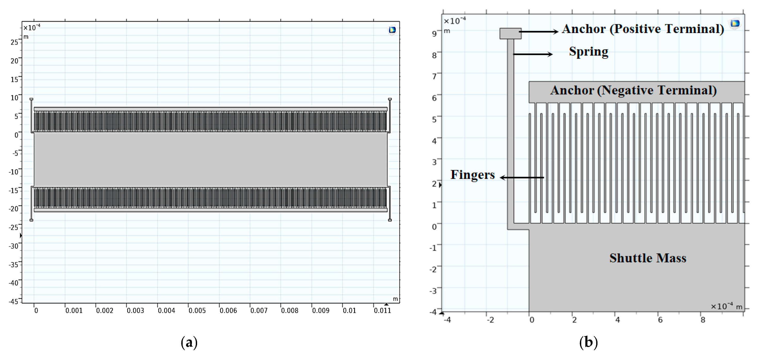
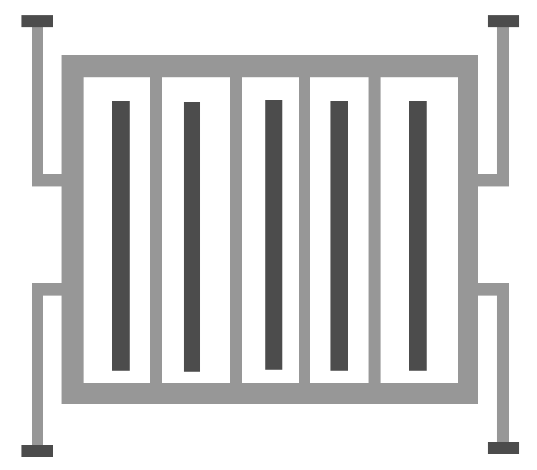
2.2. Crab Leg Spring Design
3. Calibration of COMSOL MultiPhysics 5.4
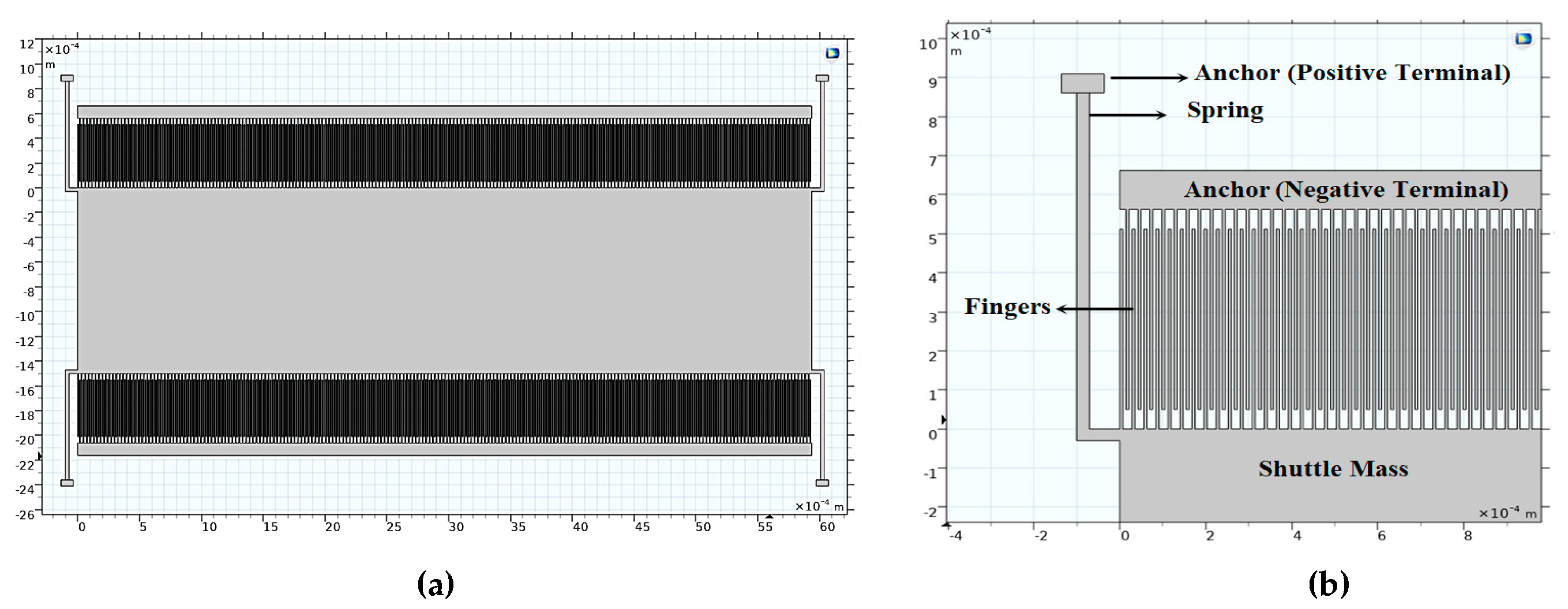
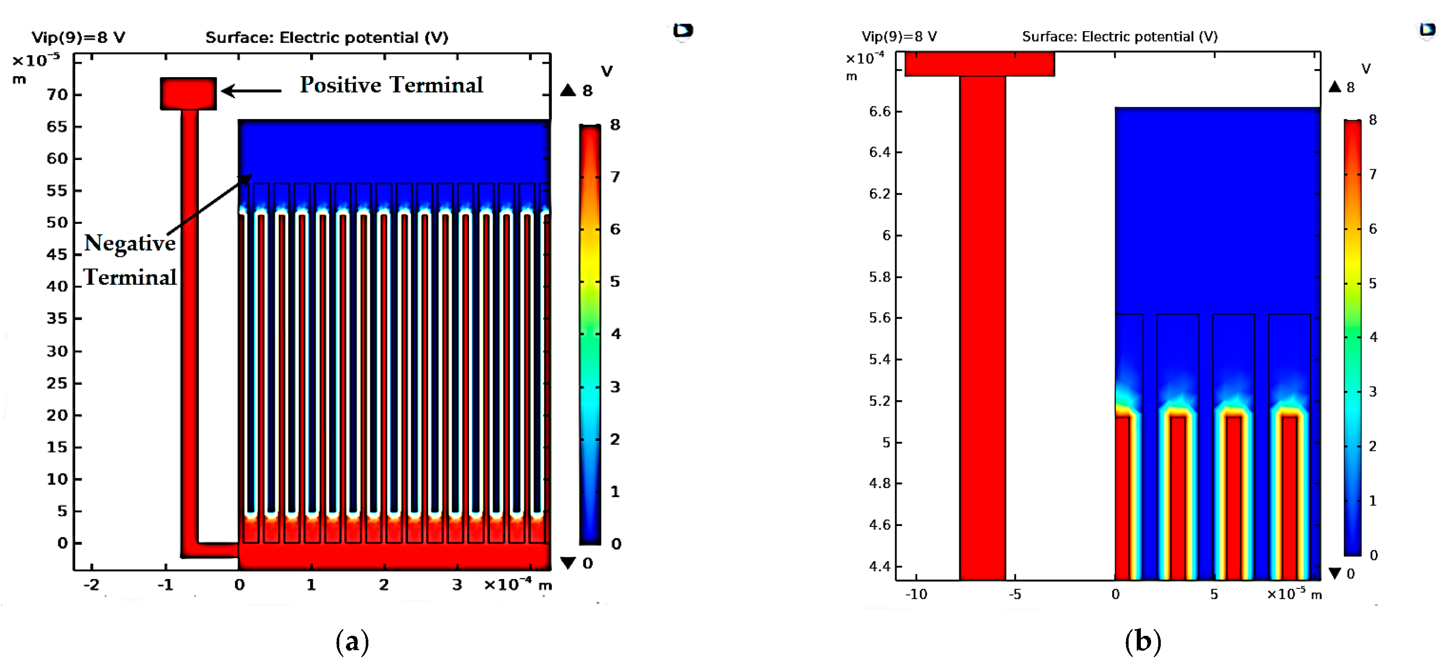
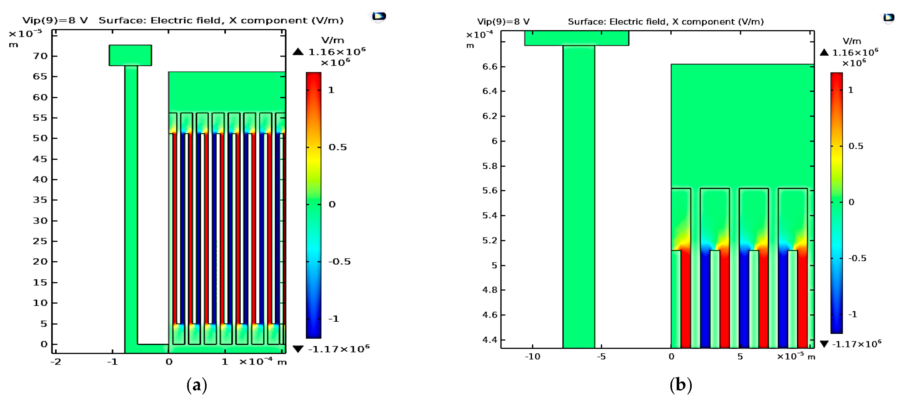
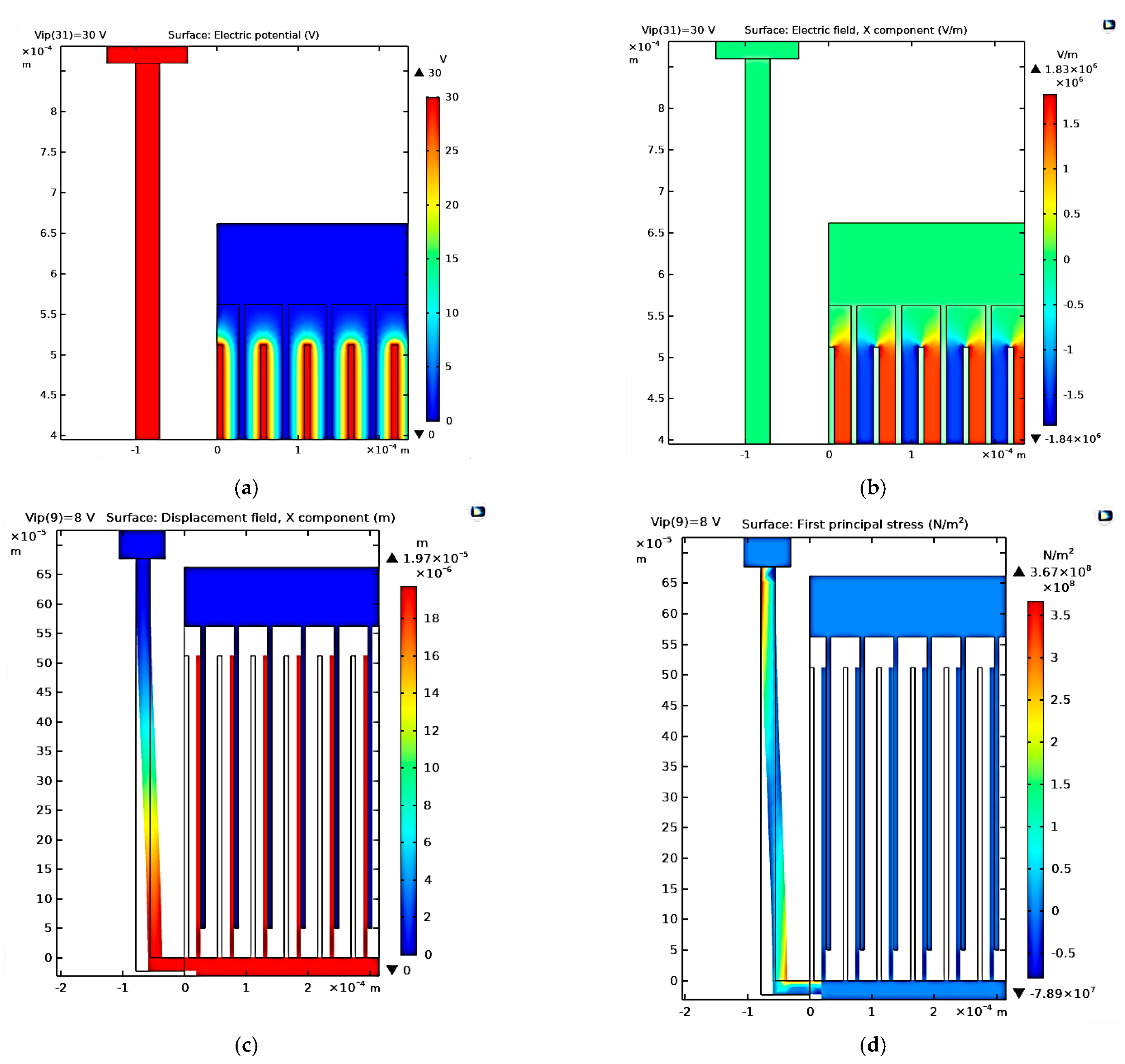
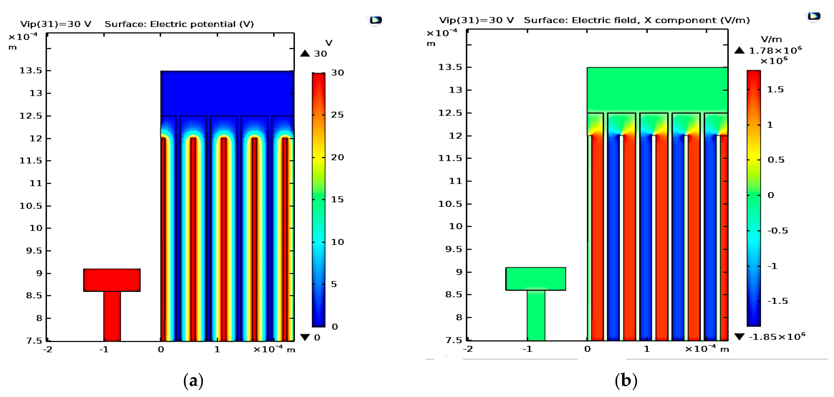
3.1. The Electric Potential and Electric Field Distributions
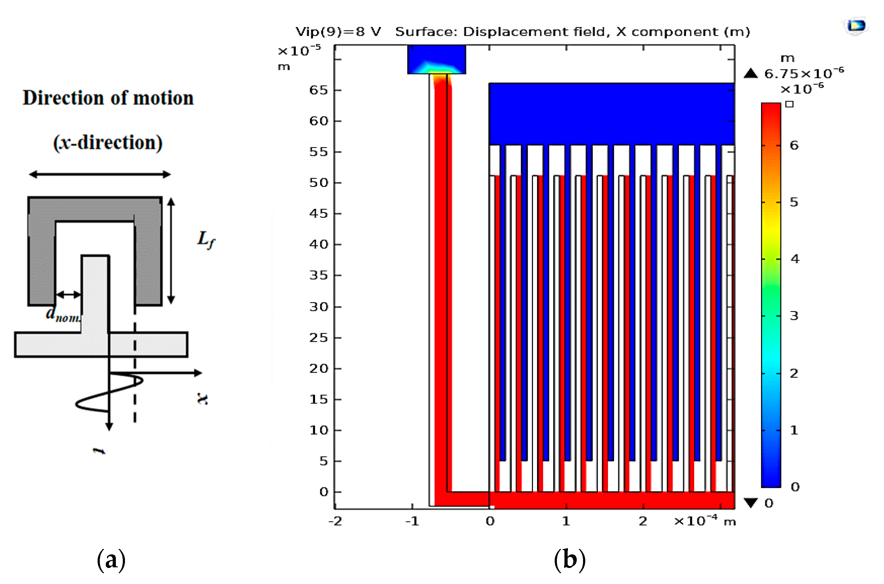
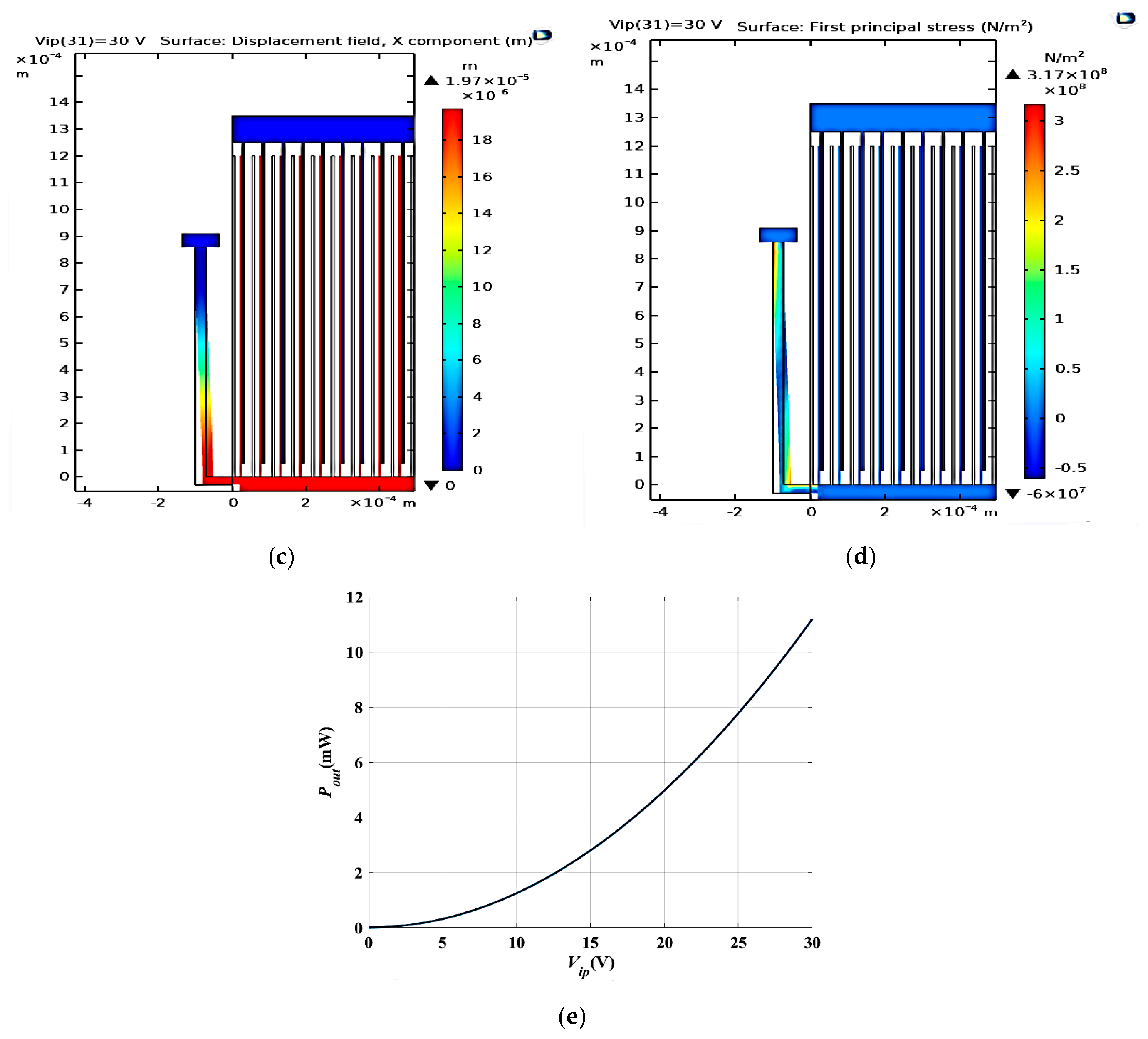
3.2. The Converter Displacement due to the Input Vibration Signal
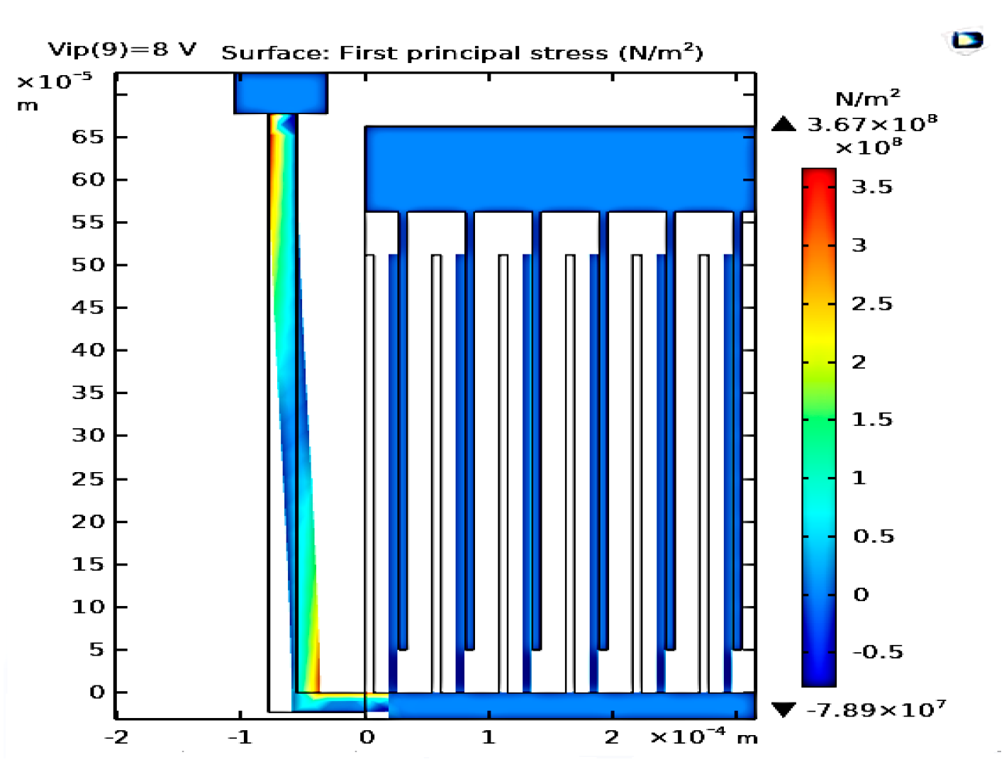
3.3. The Stress Analysis for the Converter due to the Input Vibration Signal
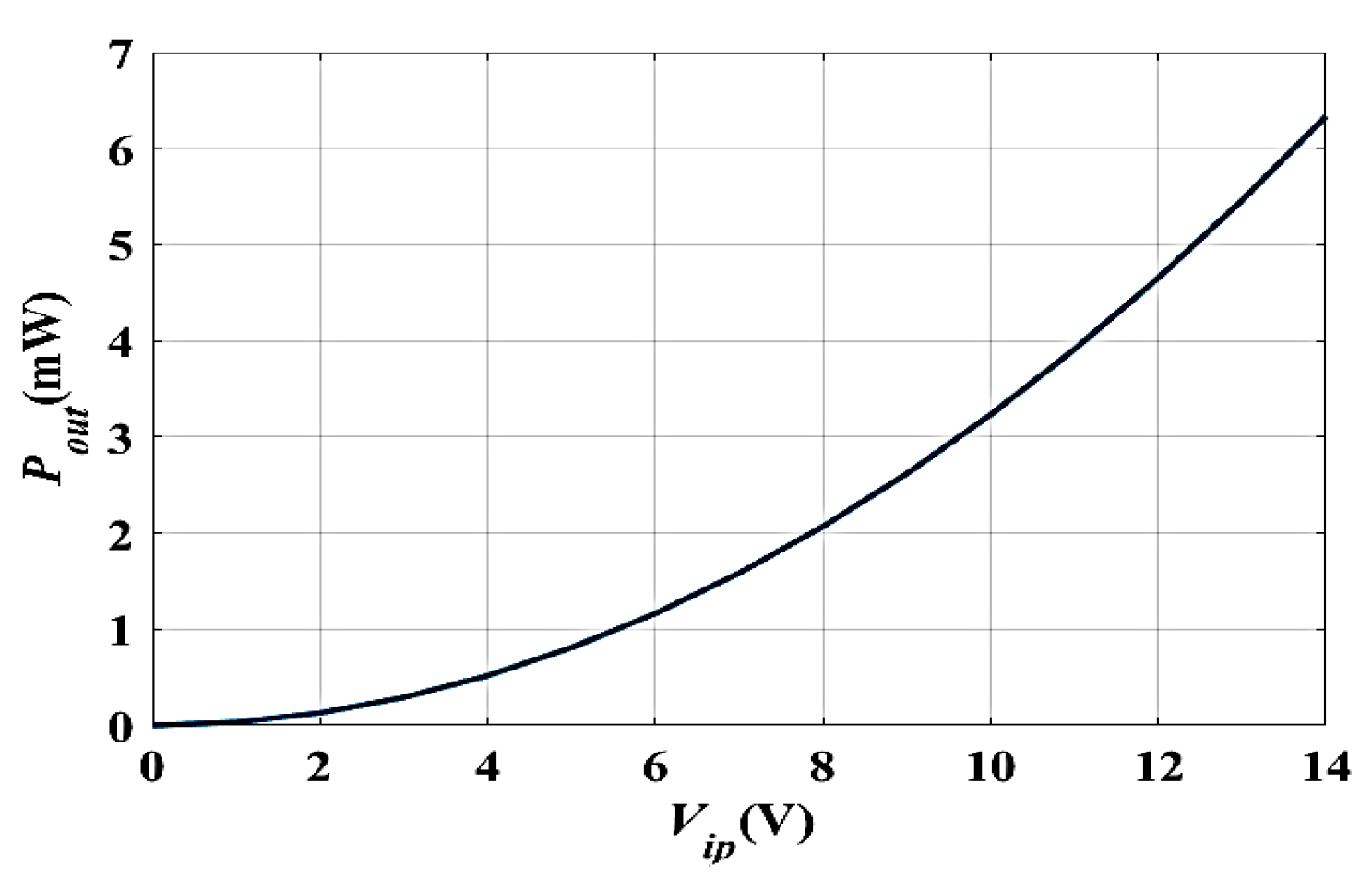
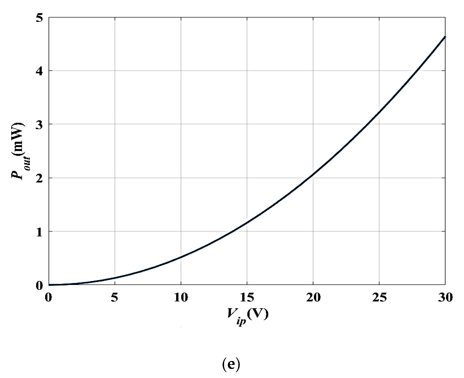
3.4. The Converter Outputs Power at Different Vip
4. Qualitative Analysis of the Three Performance-Enhancing Techniques
5. Enhancing the Converter Performance Using COMSOL Simulations
5.1. Scaling up the Technology
5.2. Technological Parameters Optimization
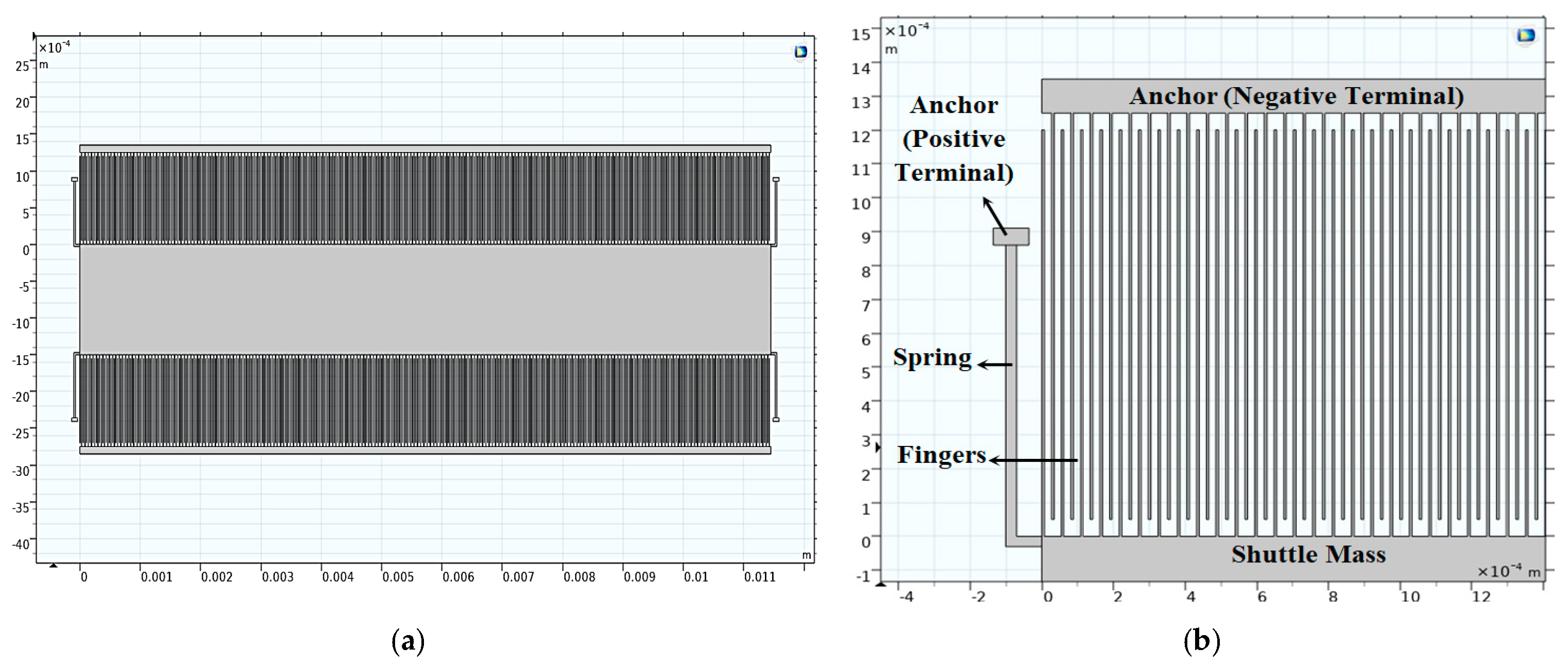
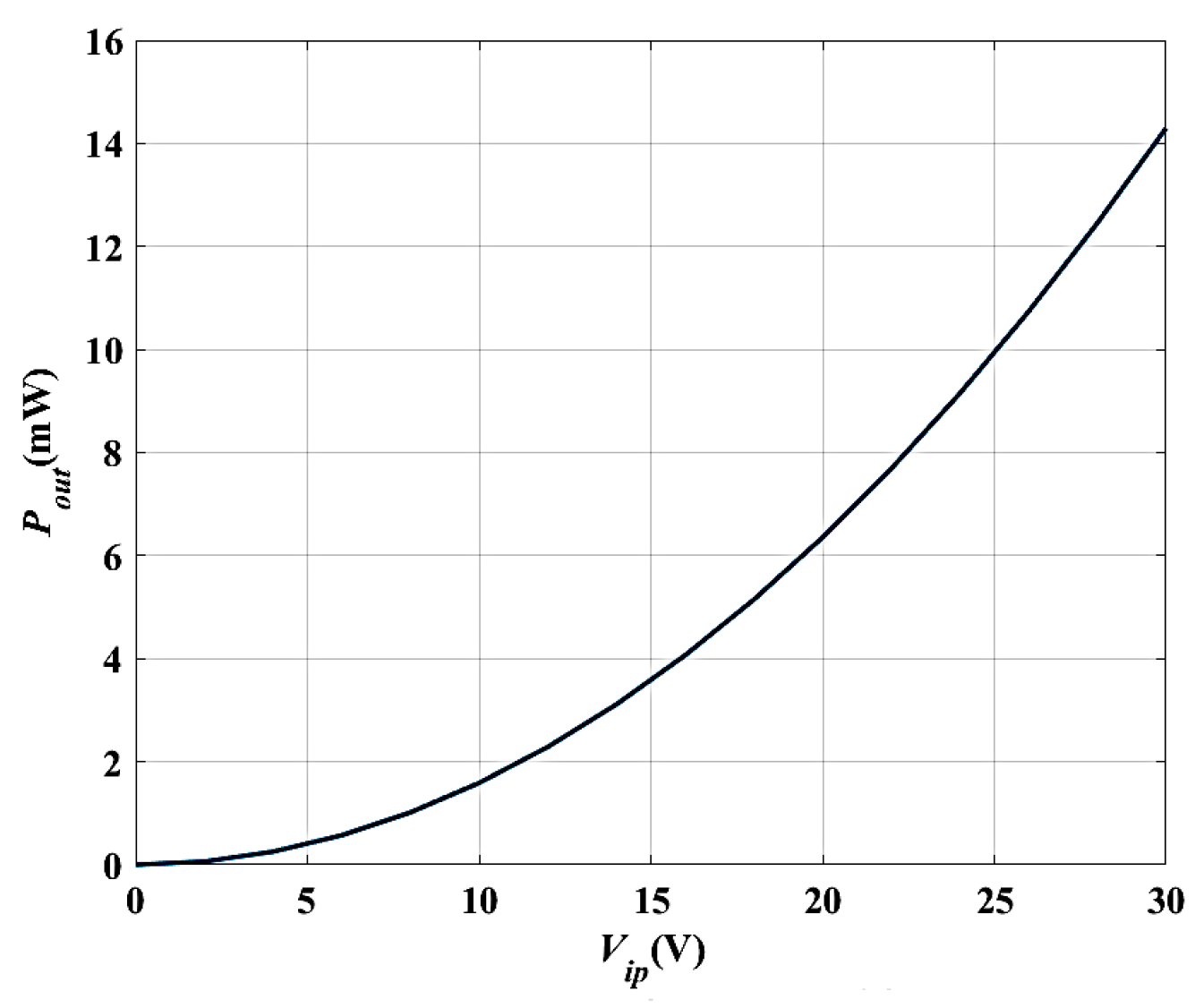
5.3. The Electrostatic MEMS Converter Structure Optimization
6. Conclusions
Supplementary Materials
Author Contributions
Funding
Data Availability Statement
Conflicts of Interest
References
- Sullivan, J.L.; Gaines, L. A Review of Battery Life-Cycle Analysis: State of Knowledge and Critical Needs; Technical Report; Argonne National Lab (ANL): Argonne, IL, USA, 2010. [Google Scholar] [CrossRef] [Green Version]
- Paulo, J.; Gaspar, P.D. Review and future trend of energy harvesting methods for portable medical devices. In Proceedings of the World Congress on Engineering, London, UK, 30 June–2 July 2010. [Google Scholar]
- Shaikh, F.K.; Zeadally, S. Energy harvesting in wireless sensor networks: A comprehensive review. Renew. Sustain. Energy Rev. 2016, 55, 1041–1054. [Google Scholar] [CrossRef]
- Davidson, J.; Mo, C. Recent advances in energy harvesting technologies for structural health monitoring applications. Recent Adv. Energy Harvest. Technol. Struct. Health Monit. Appl. 2014, 2014, 410316. [Google Scholar] [CrossRef]
- Ng, C.H.; Lim, H.N.; Hayase, S.; Zainal, Z.; Huang, N.M. Photovoltaic performances of mono-and mixed-halide structures for perovskite solar cell: A review. Renew. Sustain. Energy Rev. 2018, 90, 248–274. [Google Scholar] [CrossRef]
- Yang, Y.; Wang, S.; Stein, P.; Xu, B.X.; Yang, T. Vibration based energy harvesting with a clamped piezoelectric circular diaphragm: Analysis and identification of optimal structural parameters. Smart Mater. Struct. 2017, 26, 045011. [Google Scholar] [CrossRef]
- Ando Junior, O.H.; Maran, A.L.O.; Henao, N.C. A review of the development and applications of thermoelectric microgenerators for energy harvesting. Renew. Sustain. Energy Rev. 2018, 91, 376–393. [Google Scholar] [CrossRef]
- Wang, H.; Jasim, A.; Chen, X. Energy harvesting technologies in roadway and bridge for different applications: A comprehensive review. Appl. Energy 2018, 212, 1083–1094. [Google Scholar] [CrossRef]
- Fang, S.; Fu, X.; Du, X.; Liao, W.H. A music-box-like extended rotational plucking energy harvester with multiple piezoelectric cantilevers. Appl. Phys. Lett. 2019, 114, 233902. [Google Scholar] [CrossRef]
- Jung, I.; Shin, Y.H.; Kim, S.; Choi, J.Y.; Kang, C.Y. Flexible piezoelectric polymer-based energy harvesting system for roadway applications. Appl. Energy 2017, 197, 222–229. [Google Scholar] [CrossRef]
- Tan, Q.; Fan, K.; Tao, K.; Zhao, L.; Cai, M. A two-degree-of-freedom string-driven rotor for efficient energy harvesting from ultra-low frequency excitations. Energy 2020, 196, 117107. [Google Scholar] [CrossRef]
- Tao, K.; Wu, J.; Tang, L.; Xia, X.; Lye, S.W.; Miao, J.; Hu, X. A novel two-degree-of-freedom MEMS electromagnetic vibration energy harvester. J. Micromech. Microeng. 2016, 26, 035020. [Google Scholar] [CrossRef]
- Naruse, Y.; Matsubara, N.; Mabuchi, K.; Izumi, M.; Suzuki, S. Electrostatic micro power generation from low-frequency vibration such as human motion. J. Micromech. Microeng. 2009, 19, 094002. [Google Scholar] [CrossRef]
- Arroyo, E.; Badel, A.; Formosa, F.; Wu, Y.; Qiu, J. Comparison of electromagnetic and piezoelectric vibration energy harvesters: Model and experiments. Sens. Actuators A Phys. 2012, 183, 148–156. [Google Scholar] [CrossRef]
- Beeby, S.P.; Wang, L.; Zhu, D.; Weddell, A.S.; Merrett, G.V.; Stark, B.; Szarka, G.; Al-Hashimi, B.M. A comparison of power output from linear and nonlinear kinetic energy harvesters using real vibration data. Smart Mater. Struct. 2013, 22, 075022. [Google Scholar] [CrossRef] [Green Version]
- Sojan, S.; Kulkarni, R.K. A Comprehensive Review of energy harvesting techniques and its potential applications. Int. J. Comput. Appl. 2016, 139, 14–19. [Google Scholar] [CrossRef]
- Zhang, Y.; Wang, T.; Luo, A.; Hu, Y.; Li, X.; Wang, F. Micro electrostatic energy harvester with both broad bandwidth and high normalized power density. Appl. Energy 2018, 212, 362–371. [Google Scholar] [CrossRef]
- Sundriyal, P.; Bhattacharya, S. Energy harvesting techniques for powering wireless sensor networks in aircraft applications: A review. In Sensors for Automotive and Aerospace Applications; Springer: Singapore, 2019; pp. 55–76. [Google Scholar]
- Meninger, S.; Miranda, J.M.; Chandrakasan, J.L.A.; Slocum, A.; Schmidt, M.; Amirtharajah, R. Vibration to electric energy conversion. IEEE Trans. Very Large Scale Integr. (VLSI) Syst. 2001, 9, 64–76. [Google Scholar] [CrossRef]
- Roundy, S.; Wright, P.K.; Rabaey, J. A study of low level vibrations as a power source for wireless sensor nodes. Comput. Commun. 2003, 26, 1131–1144. [Google Scholar] [CrossRef]
- Boisseau, S.; Despesse, G.; Seddik, B.A. Electrostatic Conversion for Vibration Energy Harvesting, Small-Scale Energy Harvesting, 5th ed.; Lallart, M., Ed.; LETI, CEA, Minatec Campus: Grenoble, France, 2012. [Google Scholar] [CrossRef] [Green Version]
- Aljadiri, R.T.; Taha, L.Y.; Ivey, P. Electrostatic harvester for wind energy harvesting and wind speed remote sensing. In Proceedings of the 2015 IEEE 28th Canadian Conference on Electrical and Computer Engineering (CCECE), Halifax, NS, Canada, 3–6 May 2015. [Google Scholar] [CrossRef]
- Taylor, S.G.; Park, G.; Farinholt, K.M.; Todd, M.D. Diagnostics for piezoelectric transducers under cyclic loads deployed for structural health monitoring applications. Smart Mater. Struct. 2013, 22, 025024. [Google Scholar] [CrossRef]
- Elliott, A.D.T.; Miller, L.M.; Halvorsen, E.; Wright, P.K.; Mitcheson, P.D. Which is better, electrostatic or piezoelectric energy harvesting systems? J. Phys. Conf. Ser. 2015, 660, 012128. [Google Scholar] [CrossRef] [Green Version]
- Aljadiri, R.T.; Taha, L.Y.; Ivey, P. Electrostatic Energy Harvesting Systems: A Better Understanding of Their Sustainability. J. Clean Energy Technol. 2017, 5, 5. [Google Scholar] [CrossRef] [Green Version]
- Guillemet, R.; Basset, P.; Galayko, D.; Marty, F.; Bourouina, T. Efficient inplane gapclosing MEMS electrostatic vibration energy harvester. In Proceedings of the Power MEMS 2012, Atlanta, GA, USA, 2–5 December 2012; pp. 137–140. [Google Scholar]
- Demirhan, G. Resonance-Based Mems Temperature Sensors for Temperature Compensation of Mems Capacitive Accelerometer. Master’s Thesis, Middle East Technical University, Ankara, Turkey, 2016. [Google Scholar]
- Hsieh, K.Y.; Chiu, J.; Lu, M.S.C. Development of CMOS micromachined capacitive squeeze-film pressure sensors. IEEE Sens. J. 2017, 20, 9698–9705. [Google Scholar] [CrossRef]
- Algamili, A.S.; Khir, M.H.M.; Dennis, J.O.; Ahmed, A.Y.; Alabsi, S.S.; Hashwan, S.S.B.; Junaid, M.M. A review of actuation and sensing mechanisms in mems-based sensor devices. Nanoscale Res. Lett. 2021, 16, 1–21. [Google Scholar] [CrossRef]
- Jeong, B.; Kim, M.O.; Lee, J.I.; Eun, Y.; Choi, J.; Kim, J. Development of MEMS multi-mode electrostatic energy harvester based on the SOI process. Micromachines 2017, 8, 51. [Google Scholar] [CrossRef] [Green Version]
- Honma, H.; Mitsuya, H.; Hashiguchi, G.; Fujita, H.; Toshiyoshi, H. Improvement of energy conversion effectiveness and maximum output power of electrostatic induction-type MEMS energy harvesters by using symmetric comb-electrode structures. J. Micromech. Microeng. 2018, 28, 064005. [Google Scholar] [CrossRef]
- Naito, Y.; Uenishi, K. Electrostatic MEMS vibration energy harvesters inside of tire treads. Sensors 2019, 19, 890. [Google Scholar] [CrossRef] [Green Version]
- Karami, A. Study of Electrical Interfaces for Electrostatic Vibration Energy Harvesting. Ph.D. Thesis, Sorbonne Université, Paris, France, 2018. [Google Scholar]
- Ryalat, M.; Salim Damiri, H.; ElMoaqet, H.; AlRabadi, I. An Improved Passivity-based Control of Electrostatic MEMS Device. Micromachines 2020, 11, 688. [Google Scholar] [CrossRef]
- Hasan, M.H.; Abbasalipour, A.; Nikfarjam, H.; Pourkamali, S.; Emad-Un-Din, M.; Jafari, R.; Alsaleem, F. Exploiting pull-in/pull-out hysteresis in electrostatic MEMS sensor networks to realize a novel sensing continuous-time recurrent neural network. Micromachines 2021, 12, 268. [Google Scholar] [CrossRef]
- Syms, R.; Bouchaala, A. Mechanical Synchronization of MEMS Electrostatically Driven Coupled Beam Filters. Micromachines 2021, 12, 1191. [Google Scholar] [CrossRef]
- Chiu, Y.; Kuo, C.T.; Chu, Y.S. Design and fabrication of a micro electrostatic vibration-to-electricity energy converter. arXiv 2007, arXiv:0711.3313. [Google Scholar] [CrossRef]
- Salem, M.S.; Zekry, A.; Abouelatta, M.; Shaker, A.; Salem, M.S. Validation and Evaluation of a Behavioral Circuit Model of an Enhanced Electrostatic MEMS Converter. Micromachines 2022, 13, 868. [Google Scholar] [CrossRef]
- Van Spengen, W.M. The Electrostatic Actuation of MEMS with High Voltage Amplifiers From Comb Drive Levitation and Pull-in to Dielectric Charging and Position Noise. Falco Systems Application Note, Version 1.0, March 2018.
- Gupta, S.; Pahwa, T.; Narwal, R.; Prasad, B.; Kumar, D. Optimizing the performance of MEMS electrostatic comb drive actuator with different flexure springs. In Proceedings of the 2012 COMSOL Conference, Bangalore, India, 10–12 October 2012. [Google Scholar]
- Siddaiah, N.; Prasad, G.R.K.; Pravallika, S.S.; Prasanna, G.S.; Gopal, R.R. Performance of analysis crab leg based RF MEMS switch for defense and aerospace applications. Int. J. Eng. Technol. (UAE) 2018, 7, 71–76. [Google Scholar] [CrossRef] [Green Version]
- Acar, C.; Shkel, A. Mechanical design of MEMS gyroscopes. In MEMS Vibratory Gyroscopes: Structural Approaches to Improve Robustness, Cenk Acar, Andrei Shkel; Springer: Boston, MA, USA, 2009; pp. 73–110. [Google Scholar]
- San, H.; Cheng, Z.; Deng, Z.; Zhao, Z.; Li, Y.; Chen, X. Design and simulation of MEMS based radioisotope converter with electrostatic capacitive energy conversion mechanism. In Proceedings of the 2011 6th IEEE International Conference on Nano/Micro Engineered and Molecular Systems, Kaohsiung, Taiwan, 20–23 February 2011; pp. 988–991. [Google Scholar] [CrossRef]
- Mohammed, Z.; Bojesomo, A.; Gill, W.A.; Abe, I.M.E.; Rasras, M. A crab leg suspension based dual axis MEMS accelerometer with low cross axis sensitivity. In Proceedings of the 2016 IEEE 59th International Midwest Symposium on Circuits and Systems (MWSCAS), Abu Dhabi, United Arab Emirates, 16–19 October 2016; pp. 1–4. [Google Scholar] [CrossRef]
- Available online: http://www.fbe-asic.com/documents/is-xc06.pdf (accessed on 9 April 2015).
- Abd Alameer, M.F.; Khalaf, T.H. Computational analysis for electrical breakdown in air due to streamer discharge in rod-to-plane arrangement. IOP Conf. Ser. Mater. Sci. Eng. 2020, 757, 012018. [Google Scholar] [CrossRef]
- Oxaal, J.; Hella, M.; Borca-Tasciuc, D.A. Electrostatic MEMS vibration energy harvester for HVAC applications with impact-based frequency up-conversion. J. Micromech. Microeng. 2016, 26, 124012. [Google Scholar] [CrossRef]
- Chu, Y.S.; Kuo, C.T.; Chiu, Y. A MEMS electrostatic vibration-to-electricity energy converter. In Proceedings of the PowerMEMS 2005, Tokyo, Japan, 28–30 November 2005; pp. 49–52. [Google Scholar]
- Tao, K.; Tang, L.; Wu, J.; Lye, S.W.; Chang, H.; Miao, J. Investigation of multimodal electret-based MEMS energy harvester with impact-induced nonlinearity. J. Microelectromech. Syst. 2018, 27, 276–288. [Google Scholar] [CrossRef]
- Lu, Y.; O’Riordan, E.; Cottone, F.; Boisseau, S.; Galayko, D.; Blokhina, E.; Marty, F.; Basset, P. A batch-fabricated electret-biased wideband MEMS vibration energy harvester with frequency-up conversion behavior powering a UHF wireless sensor node. J. Micromech. Microeng. 2016, 26, 124004. [Google Scholar] [CrossRef] [Green Version]
- Tao, K.; Lye, S.W.; Miao, J.; Tang, L.; Hu, X. Out-of-plane electret-based MEMS energy harvester with the combined nonlinear effect from electrostatic force and a mechanical elastic stopper. J. Micromech. Microeng. 2015, 25, 104014. [Google Scholar] [CrossRef]


| Parameter | Definition | Value (unit) |
|---|---|---|
| t | Converter thickness | 500 µm |
| Lm | Shuttle mass length | 1 cm |
| Wm | Shuttle mass width | 0.3 cm |
| Lf | Finger length | 512 µm |
| Lb | Beam length | 0.7 mm |
| La | Thigh length | 3.2 mW |
| Ws | Spring width | 3.06 mW |
| Wf | Pout Calculated | Pout Simulated |
|---|---|---|
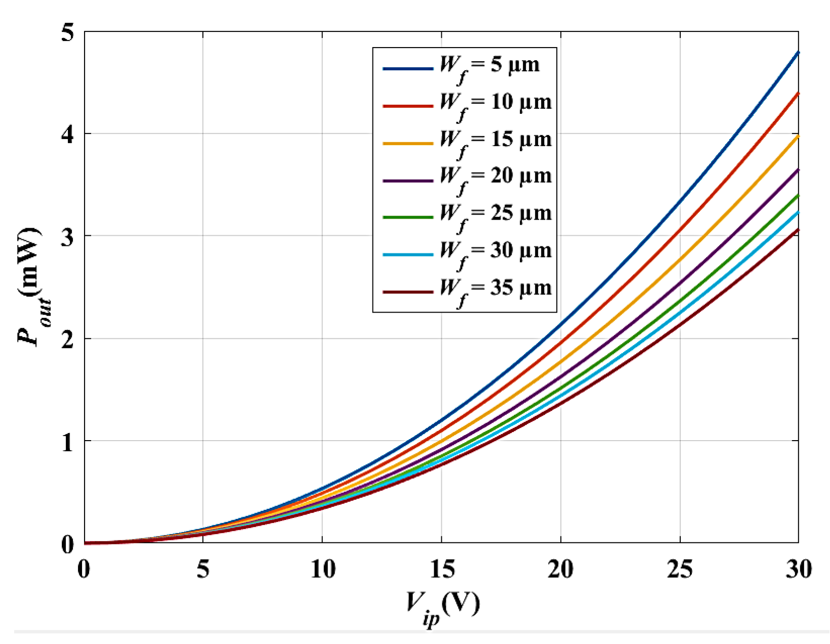
| 5 µm | 5.3 mW | 4.5 mW |
| 10 µm | 5 mW | 4.3 mW |
| 15 µm | 4.5 mW | 4 mW |
| 20 µm | 4.1 mW | 3.6 mW |
| 25 µm | 3.8 mW | 3.4 mW |
| 30 µm | 3.55 mW | 3.2 mW |
| 35 µm | 3.3 mW | 3.06 mW |
| Lf | Pout Calculated | Pout Simulated |
|---|---|---|
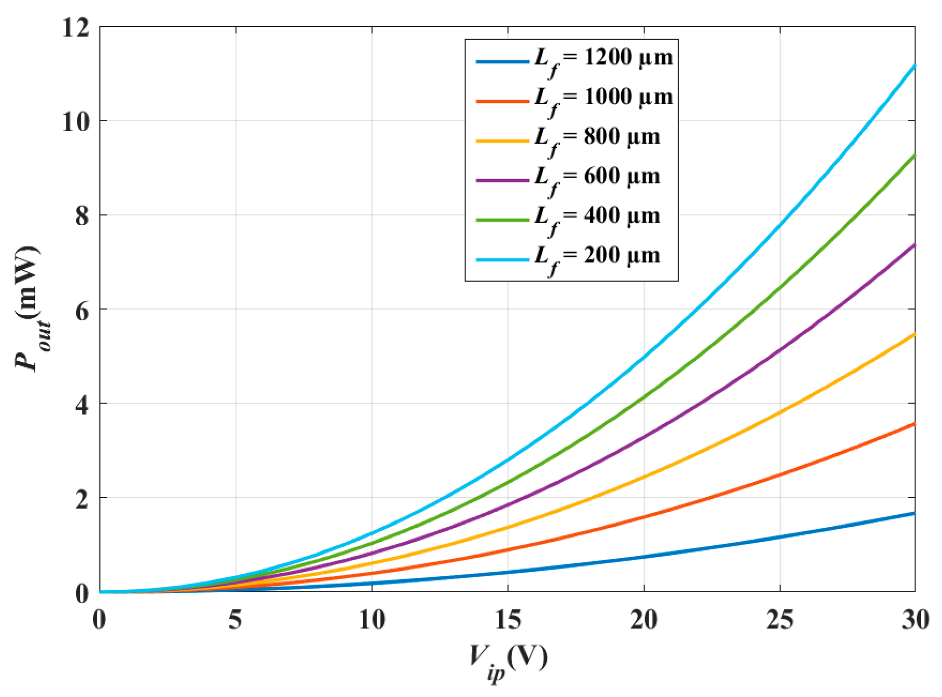
| 200 µm | 2 mW | 1.96 mW |
| 400 µm | 4.1 mW | 3.59 mW |
| 600 µm | 6.19 mW | 5.5 mW |
| 800 µm | 8.26 mW | 7.4 mW |
| 1000 µm | 10.3 mW | 9.3 mW |
| 1200 µm | 12.39 mW | 11.2 mW |
| Work | Converter Type | Frequency (kHz) | Output Power (mW) |
|---|---|---|---|
| [30] | Multi-vibrational mode | 1.272 | 0.00296 |
| [31] | Symmetric comb electrode | 0.125 | 0.070 |
| [32] | Electret vibration energy harvester | 1.2 | 0.495 |
| [47] | Gap-closing electrostatic MEMS vibration energy harvester | 0.12 | 0.00313 |
| [49] | 2DOF e-VEH MEMS device with impact-induced nonlinearity | 0.731 | 0.014 |
| [50] | Batch-fabricated, low-frequency, and wideband MEMS electrostatic vibration energy harvester | 0.428 | 0.0066 |
| [51] | Out-of-plane electret-based vibrational energy harvester | 0.95 | 0.00095 |
| This work | In-plane gap-closing converter using 0.35 µm CMOS technology | 2.5 | 2.1 |
| This work | In-plane gap-closing converter using 0.6 µm CMOS technology | 2.5 | 4.5 |
| This work | In-plane gap-closing proposed converter using 0.6 µm CMOS technology | 2.5 | 14.29 |
Disclaimer/Publisher’s Note: The statements, opinions and data contained in all publications are solely those of the individual author(s) and contributor(s) and not of MDPI and/or the editor(s). MDPI and/or the editor(s) disclaim responsibility for any injury to people or property resulting from any ideas, methods, instructions or products referred to in the content. |
© 2023 by the authors. Licensee MDPI, Basel, Switzerland. This article is an open access article distributed under the terms and conditions of the Creative Commons Attribution (CC BY) license (https://creativecommons.org/licenses/by/4.0/).
Share and Cite
Salem, M.S.; Zekry, A.; Abouelatta, M.; Shaker, A.; Salem, M.S.; Gontrand, C.; Saeed, A. Boosting the Electrostatic MEMS Converter Output Power by Applying Three Effective Performance-Enhancing Techniques. Micromachines 2023, 14, 485. https://doi.org/10.3390/mi14020485
Salem MS, Zekry A, Abouelatta M, Shaker A, Salem MS, Gontrand C, Saeed A. Boosting the Electrostatic MEMS Converter Output Power by Applying Three Effective Performance-Enhancing Techniques. Micromachines. 2023; 14(2):485. https://doi.org/10.3390/mi14020485
Chicago/Turabian StyleSalem, Mona S., Abdelhalim Zekry, Mohamed Abouelatta, Ahmed Shaker, Marwa S. Salem, Christian Gontrand, and Ahmed Saeed. 2023. "Boosting the Electrostatic MEMS Converter Output Power by Applying Three Effective Performance-Enhancing Techniques" Micromachines 14, no. 2: 485. https://doi.org/10.3390/mi14020485