
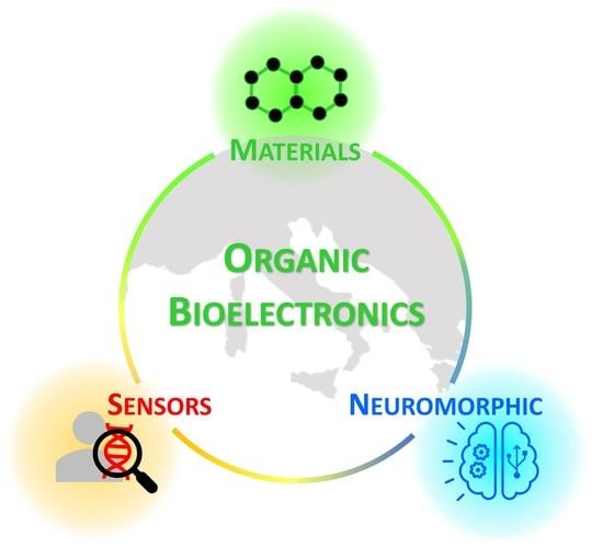
Organic Bioelectronics Development in Italy: A Review
 , , , , , , ,
Abstract
:
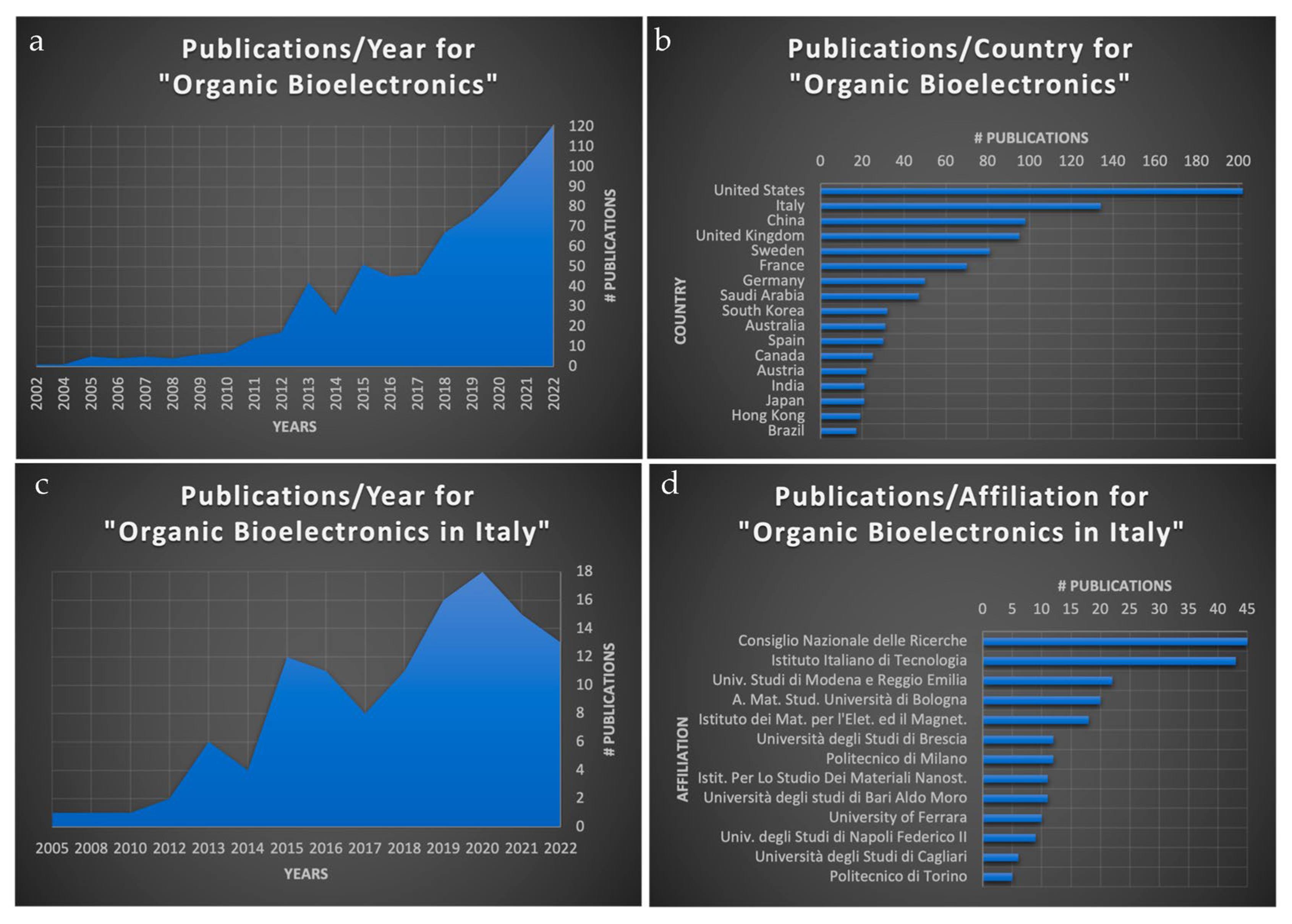
1. Introduction
2. Materials
3. Transistor-Based Sensors
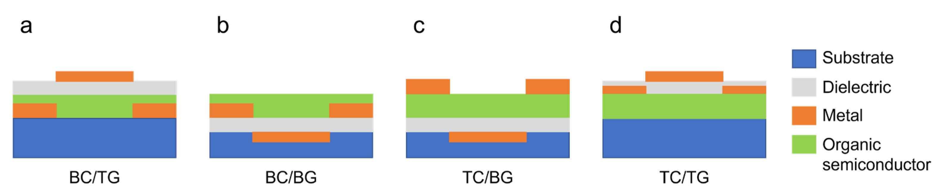
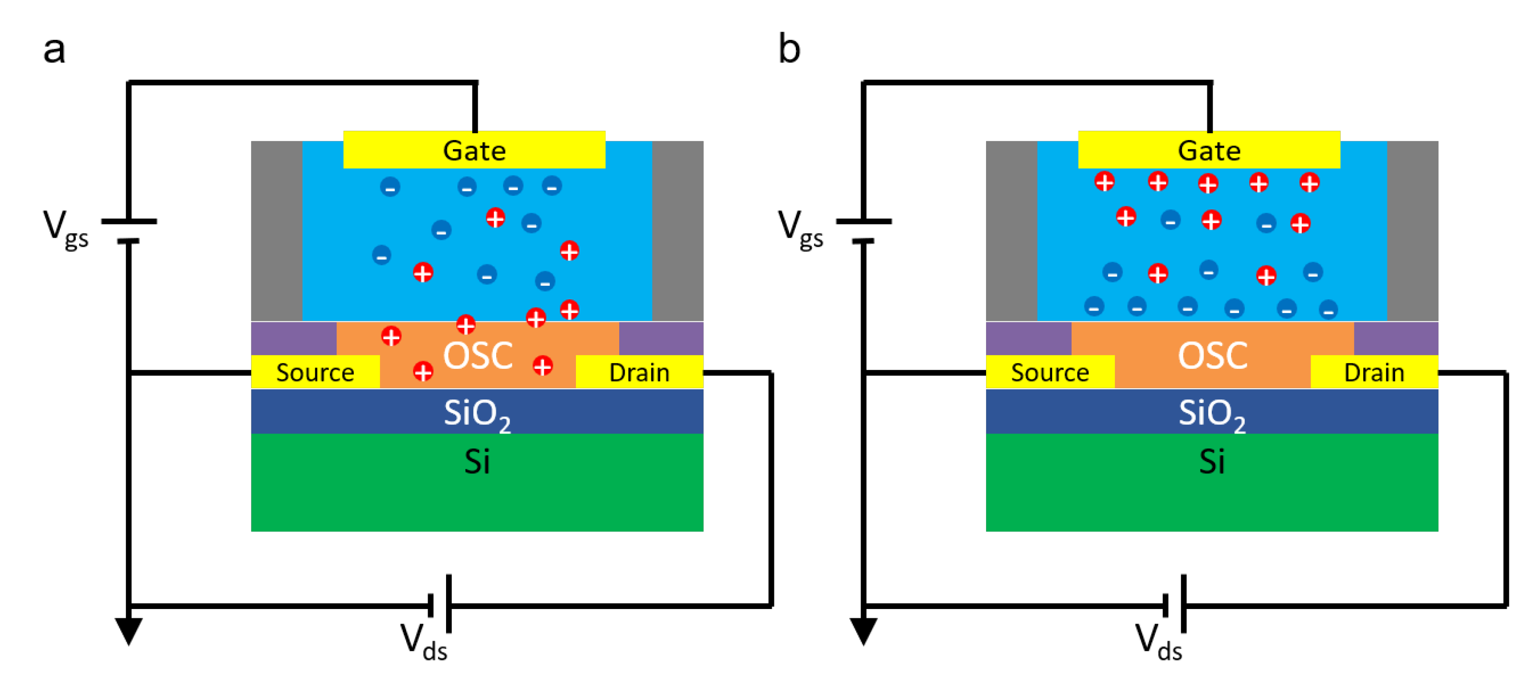
3.1. Device Structure and Working Principles
3.2. Transistor Fabrication and Modelling
3.2.1. Device Micro-Fabrication and Downscaling
3.2.2. Device Printing
3.2.3. Device Modelling
3.3. Catalytic and Immuno-Affinity-Based Sensors
3.4. Nucleic Acid Hybridization Sensors
3.5. Ions and pH-Detection Sensors
3.6. Flexible and Wearable Sensors
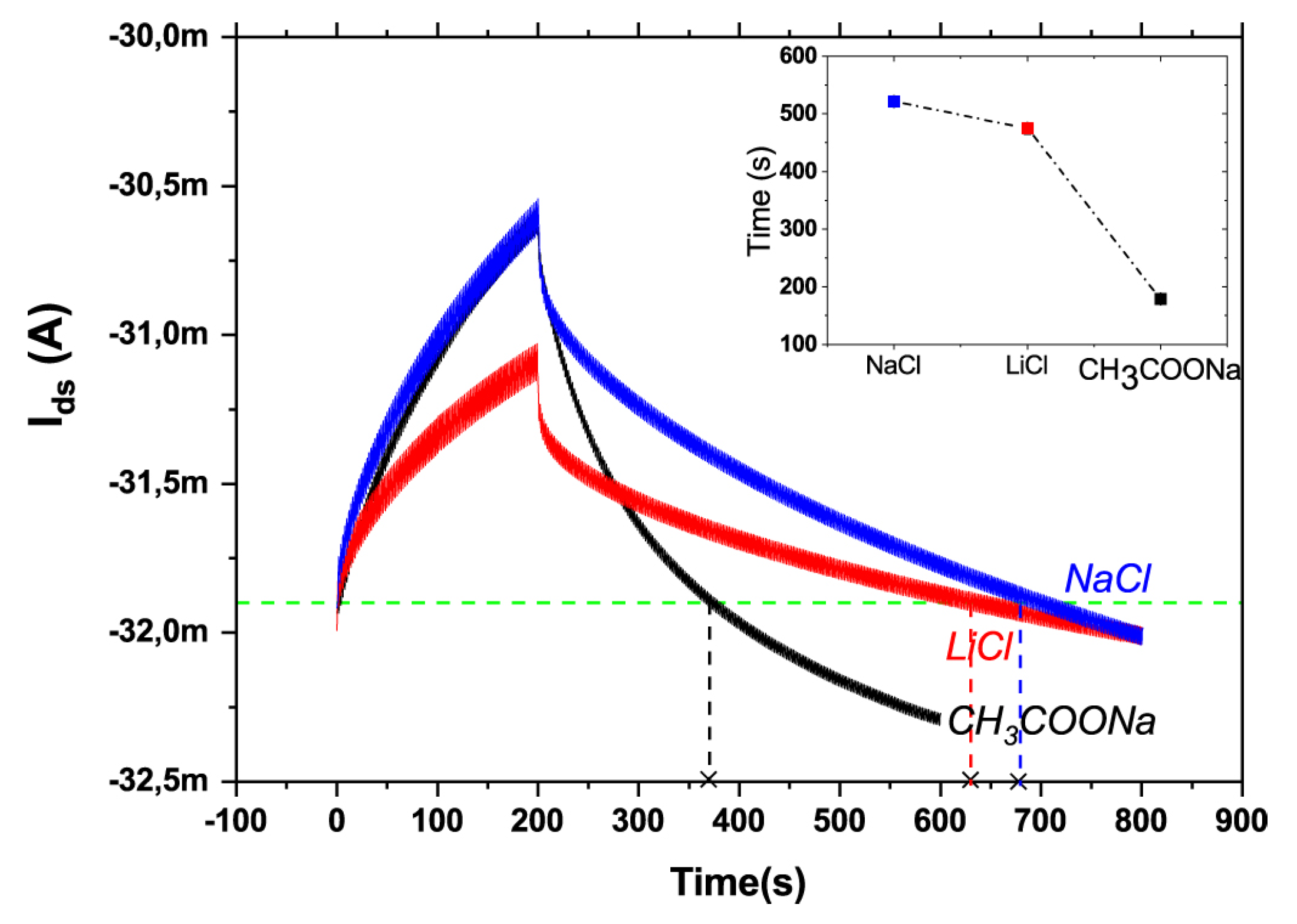
3.7. In Vivo and Cell Monitoring
4. Neuromorphic Devices
4.1. Neuromorphic Devices Development and Modelling
4.1.1. Transistor-Based Neuromorphic Devices
4.1.2. Redox-Based Memristive Devices
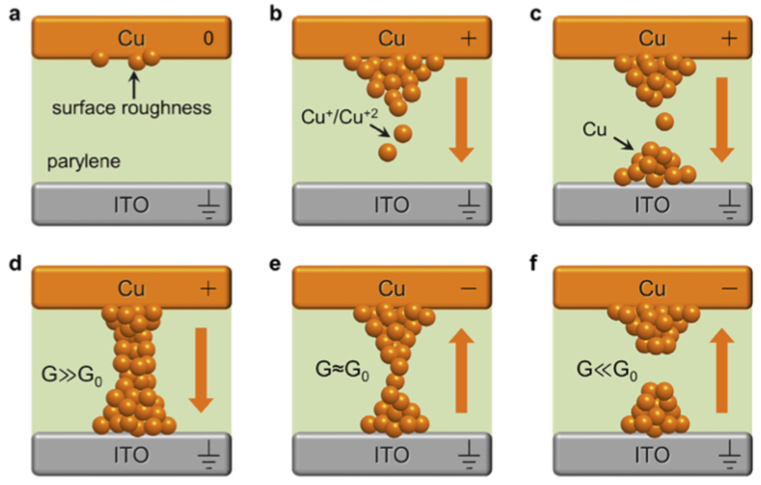
4.1.3. Filament-Based Memristive Devices
4.2. Bio-Emulating Single Devices
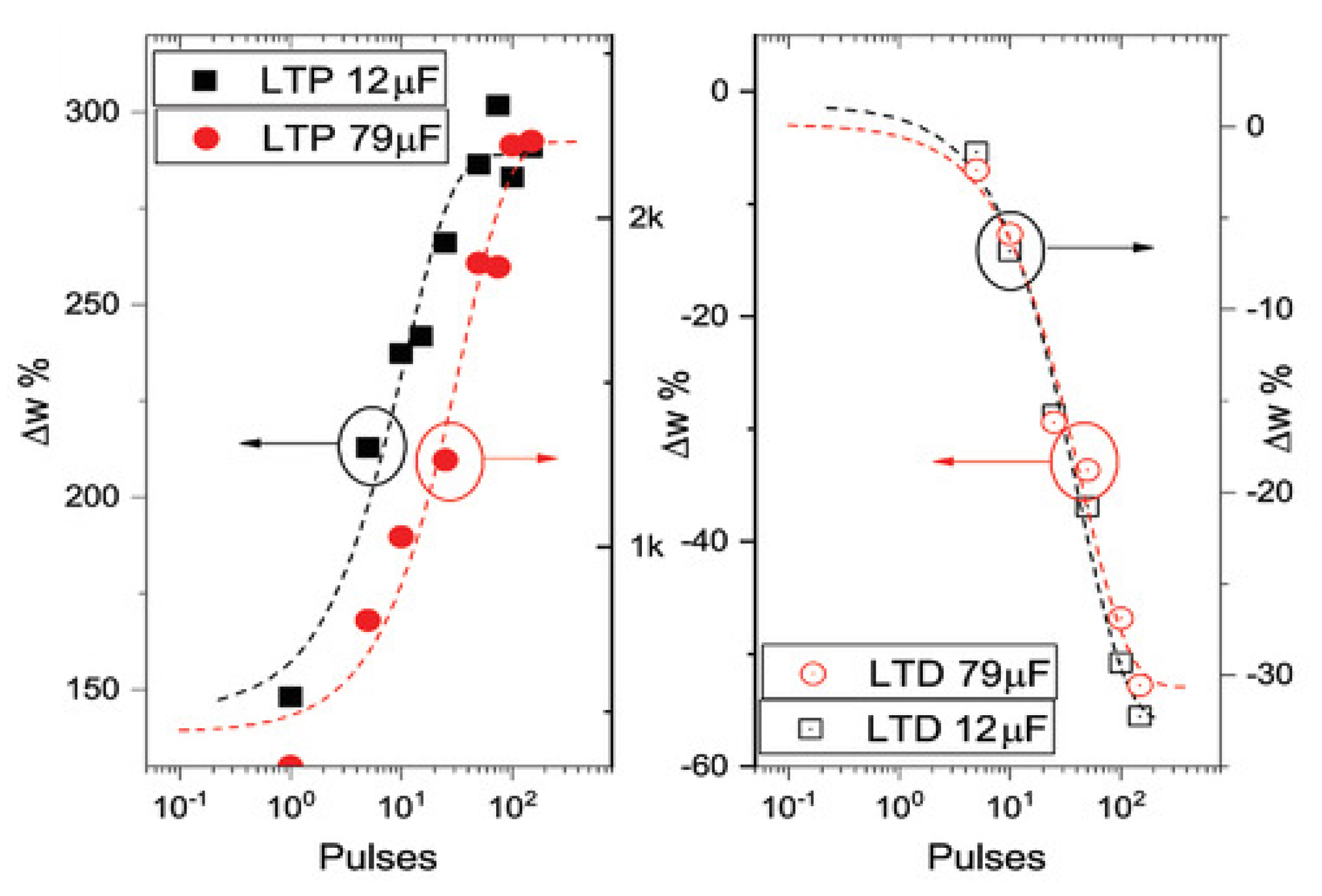
4.2.1. Devices for Emulation of Long-Term Plasticity
4.2.2. Devices for Emulation of Short-Term Plasticity
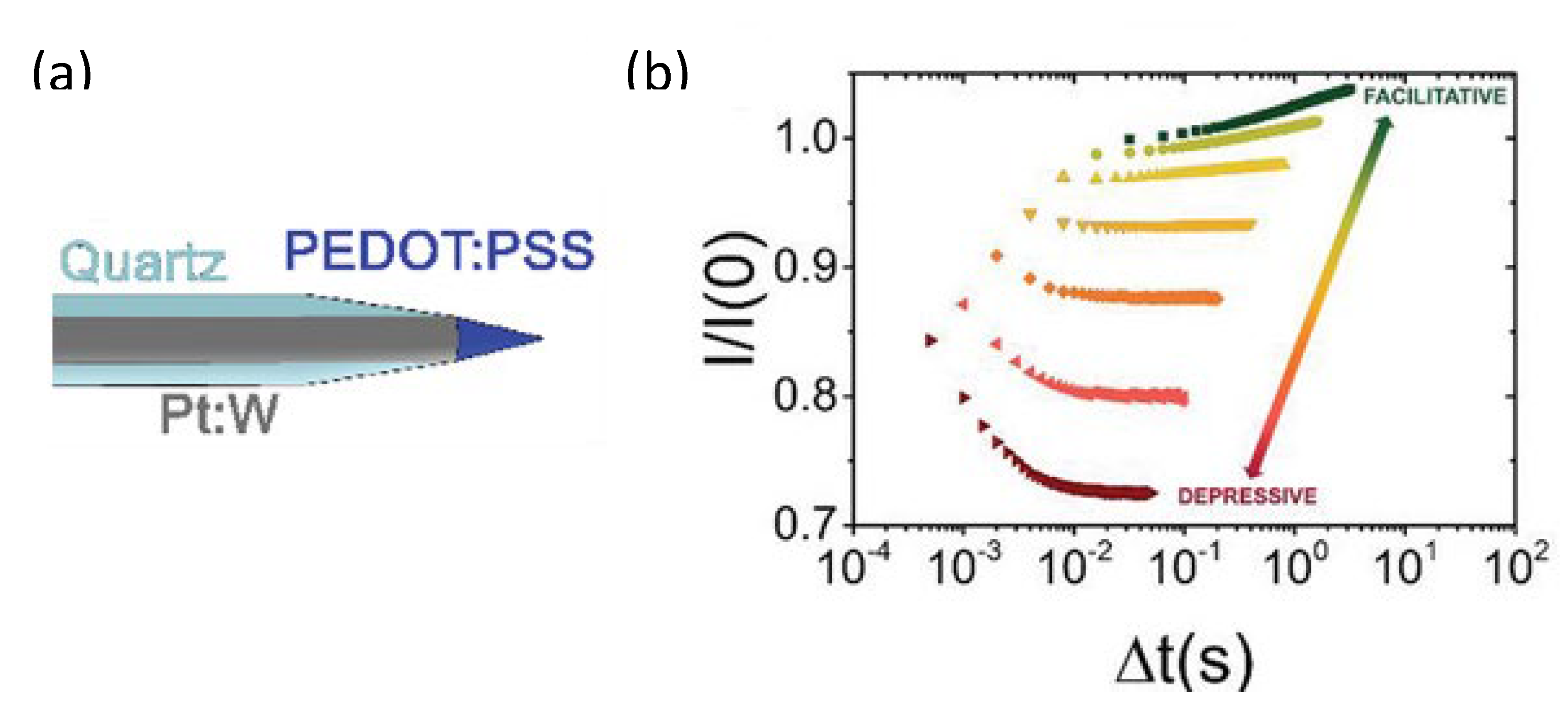
4.2.3. Devices for Spatio-Temporal Integration
4.3. Bio-Inspired Devices for Learning Algorithms
4.3.1. Supervised Learning
4.3.2. Unsupervised and Associative Learning
4.4. Devices for Coupling with Live Neurons
5. Conclusions
Author Contributions
Funding
Data Availability Statement
Conflicts of Interest
References
- D’Angelo, P.; Tarabella, G.; Romeo, A.; Marasso, S.L.; Cocuzza, M.; Peruzzi, C.; Vurro, D.; Carotenuto, G.; Iannotta, S. Nanomolar Detection of the Antitumor Drug Tamoxifen by Flexible Organic Electrochemical Devices. AIP Conf. Proc. 2018, 1990, 020015. [Google Scholar] [CrossRef]
- Battistoni, S.; Peruzzi, C.; Verna, A.; Marasso, S.L.; Cocuzza, M.; Erokhin, V.; Iannotta, S. Synaptic Response in Organic Electrochemical Transistor Gated by a Graphene Electrode. Flex. Print. Electron. 2019, 4, 044002. [Google Scholar] [CrossRef]
- Sajapin, R.; Vurro, D.; D’Angelo, P.; Tarabella, G.; Marasso, S.L.; Cocuzza, M.; Botti, M.; Buttrini, M.; Calderaro, A.; Berzina, T.; et al. Aerosol Jet Printed Organic Memristive Microdevices Based on a Chitosan: PANI Composite Conductive Channel. ACS Appl. Electron. Mater. 2022, 4, 5875–5883. [Google Scholar] [CrossRef]
- Cavallo, A.; Losi, P.; Buscemi, M.; Al Kayal, T.; Beccatelli, M.; Soldani, G.; Coppedè, N. Biocompatible Organic Electrochemical Transistor on Polymeric Scaffold for Wound Healing Monitoring. Flex. Print. Electron. 2022, 7, 035009. [Google Scholar] [CrossRef]
- Gentile, F.; Vurro, F.; Janni, M.; Manfredi, R.; Cellini, F.; Petrozza, A.; Zappettini, A.; Coppedè, N. A Biomimetic, Biocompatible OECT Sensor for the Real-Time Measurement of Concentration and Saturation of Ions in Plant Sap. Adv. Electron. Mater. 2022, 8, 200092. [Google Scholar] [CrossRef]
- Ruggiero, A.; Criscuolo, V.; Grasselli, S.; Bruno, U.; Ausilio, C.; Bovio, C.L.; Bettucci, O.; Santoro, F. Two-Photon Polymerization Lithography Enabling the Fabrication of PEDOT:PSS 3D Structures for Bioelectronic Applications. Chem. Commun. 2022, 58, 9790–9793. [Google Scholar] [CrossRef]
- Granelli, R.; Alessandri, I.; Gkoupidenis, P.; Vassalini, I.; Kovács-Vajna, Z.M.; Blom, P.W.M.; Torricelli, F. High-Performance Bioelectronic Circuits Integrated on Biodegradable and Compostable Substrates with Fully Printed Mask-Less Organic Electrochemical Transistors. Small 2022, 18, 2108077. [Google Scholar] [CrossRef]
- Torricelli, F.; Alessandri, I.; Macchia, E.; Vassalini, I.; Maddaloni, M.; Torsi, L. Green Materials and Technologies for Sustainable Organic Transistors. Adv. Mater. Technol. 2022, 7, 2100445. [Google Scholar] [CrossRef]
- Giordani, M.; Sensi, M.; Berto, M.; Di Lauro, M.; Bortolotti, C.A.; Gomes, H.L.; Zoli, M.; Zerbetto, F.; Fadiga, L.; Biscarini, F. Neuromorphic Organic Devices That Specifically Discriminate Dopamine from Its Metabolites by Nonspecific Interactions. Adv. Funct. Mater. 2020, 30, 2002141. [Google Scholar] [CrossRef]
- Di Lauro, M.; Zucchini, E.; De Salvo, A.; Delfino, E.; Bianchi, M.; Murgia, M.; Carli, S.; Biscarini, F.; Fadiga, L. A Novel Biasing Scheme of Electrolyte-Gated Organic Transistors for Safe In Vivo Amplification of Electrophysiological Signals. Adv. Mater. Interfaces 2022, 9, 2101798. [Google Scholar] [CrossRef]
- Spanu, A.; Bonfiglio, A. In Vitro Multiparametric Cellular Analysis by Micro Organic Charge-modulated Field-effect Transistor Arrays. J. Vis. Exp. 2021, 175, e62907. [Google Scholar] [CrossRef]
- Melloni, F.; Bonacchini, G.E.; Lanzani, G.; Caironi, M. Towards a Chipless and Wireless Passive System for Real-Time Encoding of the Bladder Volume. Adv. Mater. Technol. 2020, 5, 2000389. [Google Scholar] [CrossRef]
- Segantini, M.; Parmeggiani, M.; Ballesio, A.; Palmara, G.; Frascella, F.; Marasso, S.L.; Cocuzza, M. Design of a Portable Microfluidic Platform for EGOT-Based in Liquid Biosensing. Sensors 2022, 22, 969. [Google Scholar] [CrossRef]
- Nawaz, A.; Liu, Q.; Leong, W.L.; Fairfull-Smith, K.E.; Sonar, P. Organic Electrochemical Transistors for In Vivo Bioelectronics. Adv. Mater. 2021, 33, 2101874. [Google Scholar] [CrossRef]
- Shirakawa, H.; Louis, E.J.; MacDiarmid, A.G.; Chiang, C.K.; Heeger, A.J. Synthesis of electrically conducting organic polymers: Halogen derivatives of polyacetylene, (CH) x. J. Chem. Soc. Chem. Commun. 1977, 16, 578–580. [Google Scholar] [CrossRef]
- Tamburri, E.; Orlanducci, S.; Toschi, F.; Terranova, M.L.; Passeri, D. Growth Mechanisms, Morphology, and Electroactivity of PEDOT Layers Produced by Electrochemical Routes in Aqueous Medium. Synth. Met. 2009, 159, 406–414. [Google Scholar] [CrossRef]
- Gao, N.; Yu, J.; Tian, Q.; Shi, J.; Zhang, M.; Chen, S.; Zang, L. Application of PEDOT:PSS and Its Composites in Electrochemical and Electronic Chemosensors. Chemosensors 2021, 9, 79. [Google Scholar] [CrossRef]
- Kesornsit, S.; Direksilp, C.; Phasuksom, K.; Thummarungsan, N.; Sakunpongpitiporn, P.; Rotjanasuworapong, K.; Sirivat, A.; Niamlang, S. Synthesis of Highly Conductive Poly(3-Hexylthiophene) by Chemical Oxidative Polymerization Using Surfactant Templates. Polymers 2022, 14, 3860. [Google Scholar] [CrossRef]
- Namsheer, K.; Rout, C.S. Conducting Polymers: A Comprehensive Review on Recent Advances in Synthesis, Properties and Applications. RSC Adv. 2021, 11, 5659–5697. [Google Scholar] [CrossRef]
- Kim, J.S.; Chung, W.S.; Kim, K.; Kim, D.Y.; Paeng, K.J.; Jo, S.M.; Jang, S.Y. Performance Optimization of Polymer Solar Cells Using Electrostatically Sprayed Photoactive Layers. Adv. Funct. Mater. 2010, 20, 3538–3546. [Google Scholar] [CrossRef]
- Montaina, L.; Carcione, R.; Pescosolido, F.; Montalto, M.; Battistoni, S.; Tamburri, E. Three-Dimensional-Printed Polyethylene Glycol Diacrylate-Polyaniline Composites by In Situ Aniline Photopolymerization: An Innovative Biomaterial for Electrocardiogram Monitoring Systems. ACS Appl. Electron. Mater. 2023, 5, 164–172. [Google Scholar] [CrossRef]
- Battistoni, S. Organic Memristive Devices and Organic Electrochemical Transistors as Promising Elements for Bio-inspired Systems. In Memristor Computing Systems; Springer: Cham, Switzerland, 2022; pp. 273–295. [Google Scholar] [CrossRef]
- Karyakin, A.A.; Vuki, M.; Lukachova, L.V.; Karyakina, E.E.; Orlov, A.V.; Karpachova, G.P.; Wang, J. Processible Polyaniline as An Advanced Potentiometric pH Transducer. Application to Biosensors. Anal. Chem. 1999, 71, 2534–2540. [Google Scholar] [CrossRef] [PubMed]
- Wang, R.; Zhai, Q.; Zhao, Y.; An, T.; Gong, S.; Guo, Z.; Shi, Q.Q.; Yong, Z.; Cheng, W. Stretchable gold fiber-based wearable electrochemical sensor toward pH monitoring. J. Mater. Chem. B 2020, 8, 3655–3660. [Google Scholar] [CrossRef] [PubMed]
- Hou, X.; Zhou, Y.; Liu, Y.; Wang, L.; Wang, J. Coaxial electrospun flexible PANI//PU fibers as highly sensitive pH wearable sensor. J. Mater. Sci. 2020, 55, 16033–16047. [Google Scholar] [CrossRef]
- Kim, S.; Jang, Y.; Jang, M.; Lim, A.; Hardy, J.G.; Park, H.S.; Lee, J.Y. Versatile biomimetic conductive polypyrrole films doped with hyaluronic acid of different molecular weights. Acta Biomater. 2018, 80, 258–268. [Google Scholar] [CrossRef] [Green Version]
- Balint, R.; Cassidy, N.J.; Cartmell, S.H. Conductive polymers: Towards a smart biomaterial for tissue engineering. Acta Biomater. 2014, 10, 2341–2353. [Google Scholar] [CrossRef]
- Fuchiwaki, M.; Otero, T.F. Polypyrrole–para-phenolsulfonic acid/tape artificial muscle as a tool to clarify biomimetic driven reactions and ionic exchanges. J. Mater. Chem. B 2014, 2, 1954–1965. [Google Scholar] [CrossRef]
- Castro, L.E.V.; Martínez, C.J.P.; Del Castillo Castro, T.; Ortega, M.M.C.; Encinas, J.C. Chemical polymerization of pyrrole in the presence of l-serine or l-glutamic acid: Electrically controlled amoxicillin release from composite hydrogel. J. Appl. Polym. Sci. 2015, 132, 41804. [Google Scholar] [CrossRef]
- Li, S.; Qiu, Y.; Guo, X. Influence of doping anions on the ion exchange behavior of polypyrrole. J. Appl. Polym. Sci. 2009, 114, 2307–2314. [Google Scholar] [CrossRef]
- Eftekhari, A.; Kazemzad, M.; Keyanpour-Rad, M. Significant Effect of Dopant Size on Nanoscale Fractal Structure of Polypyrrole Film. Polym. J. 2006, 38, 781–785. [Google Scholar] [CrossRef] [Green Version]
- Battistoni, S.; Erokhin, V.; Iannotta, S. Emulation with organic memristive devices of impairment of LTP mechanism in neurodegenerative disease pathology. Neural Plast. 2017, 2017, 1–8. [Google Scholar] [CrossRef] [Green Version]
- Lunelli, L.; Collini, C.; Jimenez-Garduño, A.M.; Roncador, A.; Giusti, G.; Verucchi, R.; Pasquardini, L.; Iannotta, S.; Macchi, P.; Lorenzelli, L.; et al. Prototyping a memristive-based device to analyze neuronal excitability. Biophys. Chem. 2019, 253, 106212. [Google Scholar] [CrossRef]
- Tang, K.; Turner, C.; Case, L.; Mehrehjedy, A.; He, X.; Miao, W.; Guo, S. Organic Electrochemical Transistor with Molecularly Imprinted Polymer-Modified Gate for the Real-Time Selective Detection of Dopamine. ACS Appl. Polym. Mater. 2022, 4, 2337–2345. [Google Scholar] [CrossRef]
- Chen, X.; Inganäs, O. Three-step redox in polythiophenes: Evidence from electrochemistry at an ultramicroelectrode. J. Phys. Chem. 1996, 100, 15202–15206. [Google Scholar] [CrossRef]
- Tajik, S.; Beitollahi, H.; Nejad, F.G.; Shoaie, I.S.; Khalilzadeh, M.A.; Asl, M.S.; Van Le, Q.; Zhang, K.; Jang, H.W.; Shokouhimehr, M. Recent developments in conducting polymers: Applications for electrochemistry. RSC Adv. 2020, 10, 37834–37856. [Google Scholar] [CrossRef]
- Rahimzadeh, Z.; Naghib, S.M.; Zare, Y.; Rhee, K.Y. An overview on the synthesis and recent applications of conducting poly(3,4-ethylenedioxythiophene) (PEDOT) in industry and biomedicine. J. Mater. Sci. 2020 5518 2020, 55, 7575–7611. [Google Scholar] [CrossRef]
- Tremel, K.; Ludwigs, S. P3HT Revisited – From Molecular Scale to Solar Cell Devices; Springer: Cham, Switzerland, 2014; Volume 265, ISBN 978-3-662-45144-1. [Google Scholar]
- Parmeggiani, M.; Verna, A.; Ballesio, A.; Cocuzza, M.; Piatti, E.; Fra, V.; Pirri, C.F.; Marasso, S.L. P3HT Processing Study for In-Liquid EGOFET Biosensors: Effects of the Solvent and the Surface. Sensors 2019, 19, 4497. [Google Scholar] [CrossRef] [Green Version]
- Sirringhaus, H.; Brown, P.J.; Friend, R.H.; Nielsen, M.M.; Bechgaard, K.; Langeveld-Voss, B.M.W.; Spiering, A.J.H.; Janssen, R.A.J.; Meijer, E.W.; Herwig, P.; et al. Two-dimensional charge transport in self-organized, high-mobility conjugated polymers. Nature 1999, 401, 685–688. [Google Scholar] [CrossRef]
- Köhler, A.; Bässler, H. Electronic Processes in Organic Semiconductors; Wiley-VCH Verlag GmbH & Co. KGaA: Weinheim, Germany, 2015; Volume 66, ISBN 9783527685172. [Google Scholar]
- Tao, J.; Sun, W.; Lu, L. Organic small molecule semiconductor materials for OFET-based biosensors. Biosens. Bioelectron. 2022, 216, 114667. [Google Scholar] [CrossRef]
- Di Lauro, M.; Casalini, S.; Berto, M.; Campana, A.; Cramer, T.; Murgia, M.; Geoghegan, M.; Bortolotti, C.A.; Biscarini, F. The Substrate is a pH-Controlled Second Gate of Electrolyte-Gated Organic Field-Effect Transistor. ACS Appl. Mater. Interfaces 2016, 8, 31783–31790. [Google Scholar] [CrossRef] [PubMed]
- Lago, N.; Buonomo, M.; Prescimone, F.; Toffanin, S.; Muccini, M.; Cester, A. Direct Comparison of the Effect of Processing Conditions in Electrolyte-Gated and Bottom-Gated TIPS-Pentacene Transistors. Electron. Mater. 2022, 3, 281–290. [Google Scholar] [CrossRef]
- Zhang, Q.; Leonardi, F.; Casalini, S.; Temiño, I.; Mas-Torrent, M. High performing solution-coated electrolyte-gated organic field-effect transistors for aqueous media operation. Sci. Rep. 2016, 6, 1–10. [Google Scholar] [CrossRef] [PubMed] [Green Version]
- Bergveld, P. Thirty years of ISFETOLOGY: What happened in the past 30 years and what may happen in the next 30 years. Sensors Actuators, B Chem. 2003, 88, 1–20. [Google Scholar] [CrossRef] [Green Version]
- Parmeggiani, M.; Dev, A.; Björk, P.; Linnros, J. Electrokinetic-assisted gating in a microfluidic integrated Si nanoribbon ion sensor for enhanced sensitivity. Sensors Actuators B Chem. 2018, 262, 974–981. [Google Scholar] [CrossRef]
- Toss, H.; Suspène, C.; Piro, B.; Yassar, A.; Crispin, X.; Kergoat, L.; Pham, M.C.; Berggren, M. On the mode of operation in electrolyte-gated thin film transistors based on different substituted polythiophenes. Org. Electron. 2014, 15, 2420–2427. [Google Scholar] [CrossRef] [Green Version]
- Nketia-Yawson, B.; Ahn, H.; Jo, J.W. Understanding Effects of Ion Diffusion on Charge Carrier Mobility of Electrolyte-Gated Organic Transistor Using Ionic Liquid-Embedded Poly(3-hexylthiophene). Adv. Funct. Mater. 2022, 32, 2108215. [Google Scholar] [CrossRef]
- Bard, A.J.; Faulkner, L.R. Electrochemical Methods: Fundamentals and Applications, 2nd ed.; Wiley: New York, NY, USA, 2001. [Google Scholar]
- Larsson, O.; Laiho, A.; Schmickler, W.; Berggren, M.; Crispin, X. Controlling the dimensionality of charge transport in an organic electrochemical transistor by capacitive coupling. Adv. Mater. 2011, 23, 4764–4769. [Google Scholar] [CrossRef]
- Rivnay, J.; Inal, S.; Salleo, A.; Owens, R.M.; Berggren, M.; Malliaras, G.G. Organic electrochemical transistors. Nat. Rev. Mater. 2018, 3, 17086. [Google Scholar] [CrossRef]
- Berto, M.; Casalini, S.; Di Lauro, M.; Marasso, S.L.; Cocuzza, M.; Perrone, D.; Pinti, M.; Cossarizza, A.; Pirri, C.F.; Simon, D.T.; et al. Biorecognition in organic field effect transistors biosensors: The role of the density of states of the organic semiconductor. Anal. Chem. 2016, 88, 12330–12338. [Google Scholar] [CrossRef] [Green Version]
- Lai, S.; Viola, F.A.; Cosseddu, P.; Bonfiglio, A. Floating gate, organic field-effect transistor-based sensors towards biomedical applications fabricated with large-area processes over flexible substrates. Sensors 2018, 18, 1–12. [Google Scholar] [CrossRef]
- Picca, R.A.; Manoli, K.; Macchia, E.; Sarcina, L.; Di Franco, C.; Cioffi, N.; Blasi, D.; Österbacka, R.; Torricelli, F.; Scamarcio, G.; et al. Ultimately Sensitive Organic Bioelectronic Transistor Sensors by Materials and Device Structure Design. Adv. Funct. Mater. 2020, 30, 1904513. [Google Scholar] [CrossRef]
- Manco Urbina, P.A.; Berto, M.; Greco, P.; Sensi, M.; Borghi, S.; Borsari, M.; Bortolotti, C.A.; Biscarini, F. Physical insights from the Frumkin isotherm applied to electrolyte gated organic transistors as protein biosensors. J. Mater. Chem. C 2021, 9, 10965–10974. [Google Scholar] [CrossRef]
- Gentili, D.; D’Angelo, P.; Militano, F.; Mazzei, R.; Poerio, T.; Brucale, M.; Tarabella, G.; Bonetti, S.; Marasso, S.L.; Cocuzza, M.; et al. Integration of organic electrochemical transistors and immuno-affinity membranes for label-free detection of interleukin-6 in the physiological concentration range through antibody–antigen recognition. J. Mater. Chem. B 2018, 6, 5400–5406. [Google Scholar] [CrossRef]
- Mariani, F.; Gualandi, I.; Tessarolo, M.; Fraboni, B.; Scavetta, E. PEDOT: Dye-Based, Flexible Organic Electrochemical Transistor for Highly Sensitive pH Monitoring. ACS Appl. Mater. Interfaces 2018, 10, 22474–22484. [Google Scholar] [CrossRef]
- Segantini, M.; Ballesio, A.; Palmara, G.; Zaccagnini, P.; Frascella, F.; Garzone, G.; Marasso, S.L.; Cocuzza, M.; Parmeggiani, M. Investigation and Modeling of the Electrical Bias Stress in Electrolyte-Gated Organic Transistors. Adv. Electron. Mater. 2022, 8, 2101332. [Google Scholar] [CrossRef]
- Torricelli, F.; Adrahtas, D.Z.; Bao, Z.; Berggren, M.; Biscarini, F.; Bonfiglio, A.; Bortolotti, C.A.; Frisbie, C.D.; Macchia, E.; Malliaras, G.G.; et al. Electrolyte-gated transistors for enhanced performance bioelectronics. Nat. Rev. Methods Prim. 2021, 1, 66. [Google Scholar] [CrossRef]
- Nikolka, M. A perspective on overcoming water-related stability challenges in molecular and hybrid semiconductors. MRS Commun. 2020, 10, 98–111. [Google Scholar] [CrossRef]
- Minamiki, T.; Minami, T.; Kurita, R.; Niwa, O.; Wakida, S.I.; Fukuda, K.; Kumaki, D.; Tokito, S. Accurate and reproducible detection of proteins in water using an extended-gate type organic transistor biosensor. Appl. Phys. Lett. 2014, 104, 243703. [Google Scholar] [CrossRef]
- D’Angelo, P.; Marasso, S.L.; Verna, A.; Ballesio, A.; Parmeggiani, M.; Sanginario, A.; Tarabella, G.; Demarchi, D.; Pirri, C.F.; Cocuzza, M.; et al. Scaling Organic Electrochemical Transistors Down to Nanosized Channels. Small 2019, 15, 1902332. [Google Scholar] [CrossRef]
- Koutsouras, D.A.; Torricelli, F.; Blom, P.W.M. Submicron Vertical Channel Organic Electrochemical Transistors with Ultrahigh Transconductance. Adv. Electron. Mater. 2022, 9, 2200868. [Google Scholar] [CrossRef]
- Decataldo, F.; Gualandi, I.; Tessarolo, M.; Scavetta, E.; Fraboni, B. Transient-doped organic electrochemical transistors working in current-enhancing mode as sensing devices for low concentration of oxygen dissolved in solution. APL Mater. 2020, 8, 091103. [Google Scholar] [CrossRef]
- Ballesio, A.; Parmeggiani, M.; Verna, A.; Frascella, F.; Cocuzza, M.; Pirri, C.F.; Marasso, S.L. A novel hot embossing Graphene transfer process for flexible electronics. Microelectron. Eng. 2019, 209, 16–19. [Google Scholar] [CrossRef]
- Blasi, D.; Viola, F.; Modena, F.; Luukkonen, A.; MacChia, E.; Picca, R.A.; Gounani, Z.; Tewari, A.; Österbacka, R.; Caironi, M.; et al. Printed, cost-effective and stable poly(3-hexylthiophene) electrolyte-gated field-effect transistors. J. Mater. Chem. C 2020, 8, 15312–15321. [Google Scholar] [CrossRef]
- Lai, S.; Vlamidis, Y.; Mishra, N.; Cosseddu, P.; Mišeikis, V.; Ricci, P.C.; Voliani, V.; Coletti, C.; Bonfiglio, A. A Flexible, Transparent Chemosensor Integrating an Inkjet-Printed Organic Field-Effect Transistor and a Non-Covalently Functionalized Graphene Electrode. Adv. Mater. Technol. 2021, 6, 1–9. [Google Scholar] [CrossRef]
- Sensi, M.; Berto, M.; Candini, A.; Liscio, A.; Cossarizza, A.; Beni, V.; Biscarini, F.; Bortolotti, C.A. Modulating the Faradic Operation of All-Printed Organic Electrochemical Transistors by Facile in Situ Modification of the Gate Electrode. ACS Omega 2019, 4, 5374–5381. [Google Scholar] [CrossRef]
- Galliani, M.; Diacci, C.; Berto, M.; Sensi, M.; Beni, V.; Berggren, M.; Borsari, M.; Simon, D.T.; Biscarini, F.; Bortolotti, C.A. Flexible Printed Organic Electrochemical Transistors for the Detection of Uric Acid in Artificial Wound Exudate. Adv. Mater. Interfaces 2020, 7, 1–7. [Google Scholar] [CrossRef]
- Bertana, V.; Scordo, G.; Parmeggiani, M.; Scaltrito, L.; Ferrero, S.; Gomez, M.G.; Cocuzza, M.; Vurro, D.; D’Angelo, P.; Iannotta, S.; et al. Rapid prototyping of 3D Organic Electrochemical Transistors by composite photocurable resin. Sci. Rep. 2020, 10, 1–11. [Google Scholar] [CrossRef]
- Gentile, F.; Vurro, F.; Picelli, F.; Bettelli, M.; Zappettini, A.; Coppedè, N. A mathematical model of OECTs with variable internal geometry. Sens. Actuators A Phys. 2020, 304, 111894. [Google Scholar] [CrossRef]
- Casalini, S.; Leonardi, F.; Cramer, T.; Biscarini, F. Organic field-effect transistor for label-free dopamine sensing. Org. Electron. 2013, 14, 156–163. [Google Scholar] [CrossRef]
- Solodka, K.; Berto, M.; Ferraro, D.; Menozzi, C.; Borsari, M.; Bortolotti, C.A.; Biscarini, F.; Pinti, M. Detection of Neurofilament Light Chain with Label-Free Electrolyte-Gated Organic Field-Effect Transistors. Adv. Mater. Interfaces 2022, 9, 2102341. [Google Scholar] [CrossRef]
- Gualandi, I.; Marzocchi, M.; Achilli, A.; Cavedale, D.; Bonfiglio, A.; Fraboni, B. Textile Organic Electrochemical Transistors as a Platform for Wearable Biosensors. Sci. Rep. 2016, 6, 33637. [Google Scholar] [CrossRef] [Green Version]
- Seshadri, P.; Manoli, K.; Schneiderhan-Marra, N.; Anthes, U.; Wierzchowiec, P.; Bonrad, K.; Di Franco, C.; Torsi, L. Low-picomolar, label-free procalcitonin analytical detection with an electrolyte-gated organic field-effect transistor based electronic immunosensor. Biosens. Bioelectron. 2018, 104, 113–119. [Google Scholar] [CrossRef]
- Saggese, G.; Tambaro, M.; Vallicelli, E.A.; Strollo, A.G.M.; Vassanelli, S.; Baschirotto, A.; Matteis, M. De Comparison of Sneo-Based Neural Spike Detection Algorithms for Implantable Multi-Transistor Array Biosensors. Electronics 2021, 10, 410. [Google Scholar] [CrossRef]
- Baldacchini, C.; Montanarella, A.F.; Francioso, L.; Signore, M.A.; Cannistraro, S.; Bizzarri, A.R. A Reliable BioFET Immunosensor for Detection of p53 Tumour Suppressor in Physiological-Like Environment. Sensors 2020, 20, 6364. [Google Scholar] [CrossRef]
- Spijkman, M.-J.; Brondijk, J.J.; Geuns, T.C.T.; Smits, E.C.P.; Cramer, T.; Zerbetto, F.; Stoliar, P.; Biscarini, F.; Blom, P.W.M.; de Leeuw, D.M. Dual-Gate Organic Field-Effect Transistors as Potentiometric Sensors in Aqueous Solution. Adv. Funct. Mater. 2010, 20, 898–905. [Google Scholar] [CrossRef] [Green Version]
- Torsi, L.; Farinola, G.M.; Marinelli, F.; Tanese, M.C.; Omar, O.H.; Valli, L.; Babudri, F.; Palmisano, F.; Zambonin, P.G.; Naso, F. A sensitivity-enhanced field-effect chiral sensor. Nat. Mater. 2008, 7, 412–417. [Google Scholar] [CrossRef]
- Gualandi, I.; Tonelli, D.; Mariani, F.; Scavetta, E.; Marzocchi, M.; Fraboni, B. Selective detection of dopamine with an all PEDOT:PSS Organic Electrochemical Transistor. Sci. Rep. 2016, 6, 35419. [Google Scholar] [CrossRef]
- Tarabella, G.; Balducci, A.G.; Coppedè, N.; Marasso, S.; D’Angelo, P.; Barbieri, S.; Cocuzza, M.; Colombo, P.; Sonvico, F.; Mosca, R.; et al. Liposome sensing and monitoring by organic electrochemical transistors integrated in microfluidics. Biochim. Biophys. Acta - Gen. Subj. 2013, 1830, 4374–4380. [Google Scholar] [CrossRef]
- Khodagholy, D.; Rivnay, J.; Sessolo, M.; Gurfinkel, M.; Leleux, P.; Jimison, L.H.; Stavrinidou, E.; Herve, T.; Sanaur, S.; Owens, R.M.; et al. High transconductance organic electrochemical transistors. Nat. Commun. 2013, 4, 2133. [Google Scholar] [CrossRef] [Green Version]
- Spanu, A.; Losi, T.; Mascia, A.; Bonfiglio, A.; Caironi, M.; Cosseddu, P. Submicrometer-Channel Organic Transistors with MHz Operation Range on Flexible Substrates by a Low-Resolution Fabrication Technique. Adv. Mater. Technol. 2022, 8, 2200891. [Google Scholar] [CrossRef]
- Huang, W.; Chen, J.; Yao, Y.; Zheng, D.; Ji, X.; Feng, L.-W.; Moore, D.; Glavin, N.R.; Xie, M.; Chen, Y.; et al. Vertical organic electrochemical transistors for complementary circuits. Nature 2023, 613, 496–502. [Google Scholar] [CrossRef] [PubMed]
- Nawaz, A.; Merces, L.; Ferro, L.M.M.; Sonar, P.; Bufon, C.C.B. Impact of Planar and Vertical Organic Field-Effect Transistors on Flexible Electronics. Adv. Mater. 2023, 2204804. [Google Scholar] [CrossRef] [PubMed]
- Mariani, F.; Quast, T.; Andronescu, C.; Gualandi, I.; Fraboni, B.; Tonelli, D.; Scavetta, E.; Schuhmann, W. Needle-type organic electrochemical transistor for spatially resolved detection of dopamine. Microchim. Acta 2020, 187, 378. [Google Scholar] [CrossRef]
- Sarcina, L.; Viola, F.; Modena, F.; Picca, R.A.; Bollella, P.; Di Franco, C.; Cioffi, N.; Caironi, M.; Österbacka, R.; Esposito, I.; et al. A large-area organic transistor with 3D-printed sensing gate for noninvasive single-molecule detection of pancreatic mucinous cyst markers. Anal. Bioanal. Chem. 2022, 414, 5657–5669. [Google Scholar] [CrossRef]
- Viola, F.A.; Melloni, F.; Molazemhosseini, A.; Modena, F.; Sassi, M.; Beverina, L.; Caironi, M. A n-type, Stable Electrolyte Gated Organic Transistor Based on a Printed Polymer. Adv. Electron. Mater. 2023, 9, 2200573. [Google Scholar] [CrossRef]
- Ricci, S.; Casalini, S.; Parkula, V.; Selvaraj, M.; Saygin, G.D.; Greco, P.; Biscarini, F.; Mas-Torrent, M. Label-free immunodetection of α-synuclein by using a microfluidics coplanar electrolyte-gated organic field-effect transistor. Biosens. Bioelectron. 2020, 167. [Google Scholar] [CrossRef]
- Bernards, D.A.; Malliaras, G.G. Steady-state and transient behavior of organic electrochemical transistors. Adv. Funct. Mater. 2007, 17, 3538–3544. [Google Scholar] [CrossRef]
- Kaphle, V.; Paudel, P.R.; Dahal, D.; Radha Krishnan, R.K.; Lüssem, B. Finding the equilibrium of organic electrochemical transistors. Nat. Commun. 2020, 11, 2515. [Google Scholar] [CrossRef]
- Friedlein, J.T.; McLeod, R.R.; Rivnay, J. Device physics of organic electrochemical transistors. Org. Electron. 2018, 63, 398–414. [Google Scholar] [CrossRef]
- Macchia, E.; De Caro, L.; Torricelli, F.; Di Franco, C.; Mangiatordi, G.F.; Scamarcio, G.; Torsi, L. Why a Diffusing Single-Molecule can be Detected in Few Minutes by a Large Capturing Bioelectronic Interface. Adv. Sci. 2022, 9, 2104381. [Google Scholar] [CrossRef]
- Gualandi, I.; Tessarolo, M.; Mariani, F.; Arcangeli, D.; Possanzini, L.; Tonelli, D.; Fraboni, B.; Scavetta, E. Layered double hydroxide-modified organic electrochemical transistor for glucose and lactate biosensing. Sensors 2020, 20, 1–15. [Google Scholar] [CrossRef]
- Battista, E.; Lettera, V.; Villani, M.; Calestani, D.; Gentile, F.; Netti, P.A.; Iannotta, S.; Zappettini, A.; Coppedè, N. Enzymatic sensing with laccase-functionalized textile organic biosensors. Org. Electron. 2017, 40, 51–57. [Google Scholar] [CrossRef]
- Casalini, S.; Dumitru, A.C.; Leonardi, F.; Bortolotti, C.A.; Herruzo, E.T.; Campana, A.; De Oliveira, R.F.; Cramer, T.; Garcia, R.; Biscarini, F. Multiscale sensing of antibody-antigen interactions by organic transistors and single-molecule force spectroscopy. ACS Nano 2015, 9, 5051–5062. [Google Scholar] [CrossRef]
- Manoli, K.; Palazzo, G.; Macchia, E.; Tiwari, A.; Di Franco, C.; Scamarcio, G.; Favia, P.; Mallardi, A.; Torsi, L. Electrolyte gated TFT biosensors based on the Donnan’s capacitance of anchored biomolecules. In Proceedings of the SPIE Organic Photonics + Electronics Conference 2017, San Diego, CA, USA, 6–10 August 2017; Volume 10364, p. 103640J. [Google Scholar] [CrossRef]
- Macchia, E.; Manoli, K.; Holzer, B.; Di Franco, C.; Ghittorelli, M.; Torricelli, F.; Alberga, D.; Mangiatordi, G.F.; Palazzo, G.; Scamarcio, G.; et al. Single-molecule detection with a millimetre-sized transistor. Nat. Commun. 2018, 9, 3223. [Google Scholar] [CrossRef]
- Macchia, E.; Sarcina, L.; Driescher, C.; Gounani, Z.; Tewari, A.; Osterbacka, R.; Palazzo, G.; Tricase, A.; Kovacs Vajna, Z.M.; Viola, F.; et al. Single-Molecule Bioelectronic Label-Free Assay of both Protein and Genomic Markers of Pancreatic Mucinous Cysts’ in Whole Blood Serum. Adv. Electron. Mater. 2021, 7, 2100304. [Google Scholar] [CrossRef]
- Macchia, E.; Manoli, K.; Holzer, B.; Di Franco, C.; Picca, R.A.; Cioffi, N.; Scamarcio, G.; Palazzo, G.; Torsi, L. Selective single-molecule analytical detection of C-reactive protein in saliva with an organic transistor. Anal. Bioanal. Chem. 2019, 411, 4899–4908. [Google Scholar] [CrossRef] [Green Version]
- Berto, M.; Diacci, C.; D’Agata, R.; Pinti, M.; Bianchini, E.; Di Lauro, M.; Casalini, S.; Cossarizza, A.; Berggren, M.; Simon, D.; et al. EGOFET Peptide Aptasensor for Label-Free Detection of Inflammatory Cytokines in Complex Fluids. Adv. Biosyst. 2018, 2, 1–8. [Google Scholar] [CrossRef]
- Peruzzi, C.; Battistoni, S.; Montesarchio, D.; Cocuzza, M.; Marasso, S.L.; Verna, A.; Pasquardini, L.; Verucchi, R.; Aversa, L.; Erokhin, V.; et al. Interfacing aptamers, nanoparticles and graphene in a hierarchical structure for highly selective detection of biomolecules in OECT devices. Sci. Rep. 2021, 11, 9380. [Google Scholar] [CrossRef]
- Macchia, E.; Manoli, K.; Di Franco, C.; Picca, R.A.; Österbacka, R.; Palazzo, G.; Torricelli, F.; Scamarcio, G.; Torsi, L. Organic Field-Effect Transistor Platform for Label-Free, Single-Molecule Detection of Genomic Biomarkers. ACS Sensors 2020, 5, 1822–1830. [Google Scholar] [CrossRef]
- Selvaraj, M.; Greco, P.; Sensi, M.; Saygin, G.D.; Bellassai, N.; D’Agata, R.; Spoto, G.; Biscarini, F. Label free detection of miRNA-21 with electrolyte gated organic field effect transistors (EGOFETs). Biosens. Bioelectron. 2021, 182, 113144. [Google Scholar] [CrossRef] [PubMed]
- Napoli, C.; Lai, S.; Giannetti, A.; Tombelli, S.; Baldini, F.; Barbaro, M.; Bonfiglio, A. Electronic detection of DNA hybridization by coupling organic field-effect transistor-based sensors and hairpin-shaped probes. Sensors 2018, 18, 990. [Google Scholar] [CrossRef] [PubMed] [Green Version]
- Sensi, M.; Migatti, G.; Beni, V.; D’Alvise, T.M.; Weil, T.; Berto, M.; Greco, P.; Imbriano, C.; Biscarini, F.; Bortolotti, C.A. Monitoring DNA Hybridization with Organic Electrochemical Transistors Functionalized with Polydopamine. Macromol. Mater. Eng. 2022, 307, 2100880. [Google Scholar] [CrossRef]
- Gualandi, I.; Tessarolo, M.; Mariani, F.; Cramer, T.; Tonelli, D.; Scavetta, E.; Fraboni, B. Nanoparticle gated semiconducting polymer for a new generation of electrochemical sensors. Sens. Actuators B Chem. 2018, 273, 834–841. [Google Scholar] [CrossRef]
- Gualandi, I.; Tessarolo, M.; Mariani, F.; Tonelli, D.; Fraboni, B.; Scavetta, E. Organic Electrochemical Transistors as Versatile Analytical Potentiometric Sensors. Front. Bioeng. Biotechnol. 2019, 7, 354. [Google Scholar] [CrossRef] [Green Version]
- Romele, P.; Gkoupidenis, P.; Koutsouras, D.A.; Lieberth, K.; Kovács-Vajna, Z.M.; Blom, P.W.M.; Torricelli, F. Multiscale real time and high sensitivity ion detection with complementary organic electrochemical transistors amplifier. Nat. Commun. 2020, 11, 1–11. [Google Scholar] [CrossRef]
- Spanu, A.; Viola, F.; Lai, S.; Cosseddu, P.; Ricci, P.C.; Bonfiglio, A. A reference-less pH sensor based on an organic field effect transistor with tunable sensitivity. Org. Electron. 2017, 48, 188–193. [Google Scholar] [CrossRef]
- Lai, S.; Temiño, I.; Cramer, T.; del Pozo, F.G.; Fraboni, B.; Cosseddu, P.; Bonfiglio, A.; Mas-Torrent, M. Morphology Influence on the Mechanical Stress Response in Bendable Organic Field-Effect Transistors with Solution-Processed Semiconductors. Adv. Electron. Mater. 2018, 4, 1–9. [Google Scholar] [CrossRef]
- Viola, F.A.; Spanu, A.; Ricci, P.C.; Bonfiglio, A.; Cosseddu, P. Ultrathin, flexible and multimodal tactile sensors based on organic field-effect transistors. Sci. Rep. 2018, 8, 1–8. [Google Scholar] [CrossRef] [Green Version]
- Lai, S.; Garufi, A.; Madeddu, F.; Angius, G.; Bonfiglio, A.; Cosseddu, P. A Wearable Platform for Monitoring Wrist Flexion and Extension in Biomedical Applications Using Organic Transistor-Based Strain Sensors. IEEE Sens. J. 2019, 19, 6020–6028. [Google Scholar] [CrossRef]
- Decataldo, F.; Bonafè, F.; Mariani, F.; Serafini, M.; Tessarolo, M.; Gualandi, I.; Scavetta, E.; Fraboni, B. Oxygen Gas Sensing Using a Hydrogel-Based Organic Electrochemical Transistor for Work Safety Applications. Polymers 2022, 14, 1022. [Google Scholar] [CrossRef]
- Serafini, M.; Mariani, F.; Gualandi, I.; Decataldo, F.; Possanzini, L.; Tessarolo, M.; Fraboni, B.; Tonelli, D.; Scavetta, E. A wearable electrochemical gas sensor for ammonia detection. Sensors 2021, 21, 7905. [Google Scholar] [CrossRef]
- Coppedè, N.; Giannetto, M.; Villani, M.; Lucchini, V.; Battista, E.; Careri, M.; Zappettini, A. Ion selective textile organic electrochemical transistor for wearable sweat monitoring. Org. Electron. 2020, 78, 105579. [Google Scholar] [CrossRef]
- Errico, V.; Chiappara, C.; Arrabito, G.; Campisciano, V.; Scopelliti, M.; Gruttadauria, M.; Giacalone, F.; Pignataro, B.; Saggio, G. Low Angle Bending Detection Semi-transparent Piezoresistive Sensor. Lect. Notes Electr. Eng. 2023, 918 LNEE, 233–238. [Google Scholar] [CrossRef]
- Trovato, V.; Teblum, E.; Kostikov, Y.; Pedrana, A.; Re, V.; Nessim, G.D.; Rosace, G. Electrically conductive cotton fabric coatings developed by silica sol-gel precursors doped with surfactant-aided dispersion of vertically aligned carbon nanotubes fillers in organic solvent-free aqueous solution. J. Colloid Interface Sci. 2021, 586, 120–134. [Google Scholar] [CrossRef]
- Landi, A.; Peluso, A.; Troisi, A. Quantitative Prediction of the Electro-Mechanical Response in Organic Crystals. Adv. Mater. 2021, 33, 2008049. [Google Scholar] [CrossRef]
- Romeo, A.; Tarabella, G.; D’Angelo, P.; Caffarra, C.; Cretella, D.; Alfieri, R.; Petronini, P.G.; Iannotta, S. Drug-induced cellular death dynamics monitored by a highly sensitive organic electrochemical system. Biosens. Bioelectron. 2015, 68, 791–797. [Google Scholar] [CrossRef]
- D’Angelo, P.; Tarabella, G.; Romeo, A.; Giodice, A.; Marasso, S.; Cocuzza, M.; Ravanetti, F.; Cacchioli, A.; Petronini, P.G.; Iannotta, S. Monitoring the adaptive cell response to hyperosmotic stress by organic devices. MRS Commun. 2017, 7, 229–235. [Google Scholar] [CrossRef] [Green Version]
- Bonafè, F.; Decataldo, F.; Zironi, I.; Remondini, D.; Cramer, T.; Fraboni, B. AC amplification gain in organic electrochemical transistors for impedance-based single cell sensors. Nat. Commun. 2022, 13, 1–9. [Google Scholar] [CrossRef]
- Decataldo, F.; Giovannini, C.; Grumiro, L.; Marino, M.M.; Faccin, F.; Brandolini, M.; Dirani, G.; Taddei, F.; Lelli, D.; Tessarolo, M.; et al. Organic Electrochemical Transistors as Versatile Tool for Real-Time and Automatized Viral Cytopathic Effect Evaluation. Viruses 2022, 14, 1155. [Google Scholar] [CrossRef]
- Nicolò, C.; Parmeggiani, M.; Villata, S.; Baruffaldi, D.; Marasso, S.L.; Canavese, G.; Cocuzza, M.; Pirri, C.F.; Frascella, F. A programmable culture platform for hydrostatic stimulation and in situ pH sensing of lung cancer cells with organic electrochemical transistors. Micro Nano Eng. 2022, 16, 100147. [Google Scholar] [CrossRef]
- Campana, A.; Cramer, T.; Simon, D.T.; Berggren, M.; Biscarini, F. Electrocardiographic Recording with Conformable Organic Electrochemical Transistor Fabricated on Resorbable Bioscaffold. Adv. Mater. 2014, 26, 3874–3878. [Google Scholar] [CrossRef] [PubMed]
- Amato, D.; Montanaro, G.; Vurro, F.; Coppedé, N.; Briglia, N.; Petrozza, A.; Janni, M.; Zappettini, A.; Cellini, F.; Nuzzo, V. Towards in vivo monitoring of ions accumulation in trees: Response of an in planta organic electrochemical transistor based sensor to water flux density, light and vapor pressure deficit variation. Appl. Sci. 2021, 11, 4729. [Google Scholar] [CrossRef]
- Diacci, C.; Abedi, T.; Lee, J.W.; Gabrielsson, E.O.; Berggren, M.; Simon, D.T.; Niittylä, T.; Stavrinidou, E. Diurnal in vivo xylem sap glucose and sucrose monitoring using implantable organic electrochemical transistor sensors. iScience 2021, 24, 101966. [Google Scholar] [CrossRef]
- Sarcina, L.; Macchia, E.; Loconsole, G.; D’Attoma, G.; Bollella, P.; Catacchio, M.; Leonetti, F.; Di Franco, C.; Elicio, V.; Scamarcio, G.; et al. Fast and Reliable Electronic Assay of a Xylella fastidiosa Single Bacterium in Infected Plants Sap. Adv. Sci. 2022, 9, 2203900. [Google Scholar] [CrossRef]
- Battistoni, S.; Cocuzza, M.; Marasso, S.L.; Verna, A.; Erokhin, V. The Role of the Internal Capacitance in Organic Memristive Device for Neuromorphic and Sensing Applications. Adv. Electron. Mater. 2021, 7, 2100494. [Google Scholar] [CrossRef]
- Giordani, M.; Di Lauro, M.; Berto, M.; Bortolotti, C.A.; Vuillaume, D.; Gomes, H.L.; Zoli, M.; Biscarini, F. Whole Organic Electronic Synapses for Dopamine Detection. In Proceedings of the SPIE Organic Photonics + Electronics Conference, San Diego, CA, USA, 28 August–1 September 2016; Kymissis, I., Shinar, R., Torsi, L., Eds.; 2016; p. 99440P. [Google Scholar]
- Keene, S.T.; Lubrano, C.; Kazemzadeh, S.; Melianas, A.; Tuchman, Y.; Polino, G.; Scognamiglio, P.; Cinà, L.; Salleo, A.; van de Burgt, Y.; et al. A biohybrid synapse with neurotransmitter-mediated plasticity. Nat. Mater. 2020, 19, 969–973. [Google Scholar] [CrossRef]
- Lapkin, D.A.; Emelyanov, A.V.; Demin, V.A.; Erokhin, V.V.; Feigin, L.A.; Kashkarov, P.K.; Kovalchuk, M.V. Polyaniline-based memristive microdevice with high switching rate and endurance. Appl. Phys. Lett. 2018, 112, 043302. [Google Scholar] [CrossRef]
- Erokhin, V.; Berzina, T.; Camorani, P.; Smerieri, A.; Vavoulis, D.; Feng, J.; Fontana, M.P. Material memristive device circuits with synaptic plasticity: Learning and memory. Bionanoscience 2011, 1, 24–30. [Google Scholar] [CrossRef]
- Cifarelli, A.; Berzina, T.; Parisini, A.; Erokhin, V.; Iannotta, S. Polysaccarides-based gels and solid-state electronic devices with memresistive properties: Synergy between polyaniline electrochemistry and biology. AIP Adv. 2016, 6, 111302. [Google Scholar] [CrossRef] [Green Version]
- Minnekhanov, A.A.; Emelyanov, A.V.; Lapkin, D.A.; Nikiruy, K.E.; Shvetsov, B.S.; Nesmelov, A.A.; Rylkov, V.V.; Demin, V.A.; Erokhin, V.V. Parylene Based Memristive Devices with Multilevel Resistive Switching for Neuromorphic Applications. Sci. Rep. 2019, 9, 10800. [Google Scholar] [CrossRef] [Green Version]
- Giordani, M.; Berto, M.; Di Lauro, M.; Bortolotti, C.A.; Zoli, M.; Biscarini, F. Specific Dopamine Sensing Based on Short-Term Plasticity Behavior of a Whole Organic Artificial Synapse. ACS Sensors 2017, 2, 1756–1760. [Google Scholar] [CrossRef]
- Malakhova, Y.N.; Korovin, A.N.; Lapkin, D.A.; Malakhov, S.N.; Shcherban, V.V.; Pichkur, E.B.; Yakunin, S.N.; Demin, V.A.; Chvalun, S.N.; Erokhin, V. Planar and 3D fibrous polyaniline-based materials for memristive elements. Soft Matter 2017, 13, 7300–7306. [Google Scholar] [CrossRef] [Green Version]
- Portilla, L.; Loganathan, K.; Faber, H.; Eid, A.; Hester, J.G.D.; Tentzeris, M.M.; Fattori, M.; Cantatore, E.; Jiang, C.; Nathan, A.; et al. Wirelessly powered large-area electronics for the Internet of Things. Nat. Electron. 2022, 6, 10–17. [Google Scholar] [CrossRef]
- Battistoni, S.; Dimonte, A.; Erokhin, V. Spectrophotometric characterization of organic memristive devices. Org. Electron. 2016, 38, 79–83. [Google Scholar] [CrossRef]
- Lapkin, D.A.; Korovin, A.N.; Malakhov, S.N.; Emelyanov, A.V.; Demin, V.A.; Erokhin, V.V. Optical Monitoring of the Resistive States of a Polyaniline-Based Memristive Device. Adv. Electron. Mater. 2020, 6, 2000511. [Google Scholar] [CrossRef]
- Battistoni, S.; Sajapin, R.; Erokhin, V.; Verna, A.; Cocuzza, M.; Marasso, S.L.; Iannotta, S. Effects of noise sourcing on organic memristive devices. Chaos Solitons Fractals 2020, 141, 110319. [Google Scholar] [CrossRef]
- Prudnikov, N.V.; Lapkin, D.A.; Emelyanov, A.V.; Minnekhanov, A.A.; Malakhova, Y.N.; Chvalun, S.N.; Demin, V.A.; Erokhin, V.V. Associative STDP-like learning of neuromorphic circuits based on polyaniline memristive microdevices. J. Phys. D. Appl. Phys. 2020, 53, 414001. [Google Scholar] [CrossRef]
- Erokhin, V.; Berzina, T.; Fontana, M.P. Hybrid electronic device based on polyaniline-polyethyleneoxide junction. J. Appl. Phys. 2005, 97, 64501. [Google Scholar] [CrossRef]
- Demin, V.A.; Erokhin, V.V.; Kashkarov, P.K.; Kovalchuk, M. V Electrochemical model of the polyaniline based organic memristive device. J. Appl. Phys. 2014, 116, 64507. [Google Scholar] [CrossRef]
- Burganova, R.; Parisini, A.; Vantaggio, S.; Sajapin, R.; Berzina, T. The role of the polyelectrolyte composition in kinetic behaviour of organic memristive device. Microelectron. Eng. 2021, 239, 111527. [Google Scholar] [CrossRef]
- Sajapin, R.; Berzina, T.; Burganova, R.; Iannotta, S. New insight in the operation mechanism of Organic Memristive Devices: The role of PEO-based polyelectrolyte solute ions. Org. Electron. 2021, 94, 106173. [Google Scholar] [CrossRef]
- Berzina, T.; Erokhin, V.; Fontana, M.P. Spectroscopic investigation of an electrochemically controlled conducting polymer-solid electrolyte junction. J. Appl. Phys. 2007, 101, 24501. [Google Scholar] [CrossRef]
- Berzina, T.; Erokhina, S.; Camorani, P.; Konovalov, O.; Erokhin, V.; Fontana, M.P. Electrochemical control of the conductivity in an organic memristor: A time-resolved X-ray fluorescence study of ionic drift as a function of the applied voltage. ACS Appl. Mater. Interfaces 2009, 1, 2115–2118. [Google Scholar] [CrossRef] [PubMed]
- Battistoni, S.; Verna, A.; Marasso, S.L.; Cocuzza, M.; Erokhin, V. On the Interpretation of Hysteresis Loop for Electronic and Ionic Currents in Organic Memristive Devices. Phys. Status Solidi Appl. Mater. Sci. 2020, 217, 1900985. [Google Scholar] [CrossRef]
- Demin, V.A.; Erokhin, V.V.; Kashkarov, P.K.; Kovalchuk, M.V. Electrochemical model of polyaniline-based memristor with mass transfer step. J. Appl. Phys. 2015, 116, 280005. [Google Scholar]
- Khodagholy, D.; Doublet, T.; Gurfinkel, M.; Quilichini, P.; Ismailova, E.; Leleux, P.; Herve, T.; Sanaur, S.; Bernard, C.; Malliaras, G.G. Highly Conformable Conducting Polymer Electrodes for In Vivo Recordings. Adv. Mater. 2011, 23, H268–H272. [Google Scholar] [CrossRef]
- Chen, Q.; Lin, M.; Wang, Z.; Zhao, X.; Cai, Y.; Liu, Q.; Fang, Y.; Yang, Y.; He, M.; Huang, R. Low Power Parylene-Based Memristors with a Graphene Barrier Layer for Flexible Electronics Applications. Adv. Electron. Mater. 2019, 5, 1800852. [Google Scholar] [CrossRef]
- Minnekhanov, A.A.; Shvetsov, B.S.; Martyshov, M.M.; Nikiruy, K.E.; Kukueva, E.V.; Presnyakov, M.Y.; Forsh, P.A.; Rylkov, V.V.; Erokhin, V.V.; Demin, V.A.; et al. On the resistive switching mechanism of parylene-based memristive devices. Org. Electron. 2019, 74, 89–95. [Google Scholar] [CrossRef]
- Battistoni, S.; Erokhin, V.; Iannotta, S. Frequency driven organic memristive devices for neuromorphic short term and long term plasticity. Org. Electron. 2019, 65, 434–438. [Google Scholar] [CrossRef]
- Gkoupidenis, P.; Schaefer, N.; Garlan, B.; Malliaras, G.G. Neuromorphic Functions in PEDOT:PSS Organic Electrochemical Transistors. Adv. Mater. 2015, 27, 7176–7180. [Google Scholar] [CrossRef]
- Lubrano, C.; Bruno, U.; Ausilio, C.; Santoro, F. Supported Lipid Bilayers Coupled to Organic Neuromorphic Devices Modulate Short-Term Plasticity in Biomimetic Synapses. Adv. Mater. 2022, 34, 2110194. [Google Scholar] [CrossRef]
- Desbief, S.; di Lauro, M.; Casalini, S.; Guerin, D.; Tortorella, S.; Barbalinardo, M.; Kyndiah, A.; Murgia, M.; Cramer, T.; Biscarini, F.; et al. Electrolyte-gated organic synapse transistor interfaced with neurons. Org. Electron. 2016, 38, 21–28. [Google Scholar] [CrossRef] [Green Version]
- Di Lauro, M.; De Salvo, A.; Sebastianella, G.C.; Bianchi, M.; Carli, S.; Murgia, M.; Fadiga, L.; Biscarini, F. Tunable Short-Term Plasticity Response in Three-Terminal Organic Neuromorphic Devices. ACS Appl. Electron. Mater. 2020, 2, 1849–1854. [Google Scholar] [CrossRef]
- Calandra Sebastianella, G.; Di Lauro, M.; Murgia, M.; Bianchi, M.; Carli, S.; Zoli, M.; Fadiga, L.; Biscarini, F. Implantable Organic Artificial Synapses Exhibiting Crossover between Depressive and Facilitative Plasticity Response. Adv. Electron. Mater. 2021, 7, 2100755. [Google Scholar] [CrossRef]
- Indiveri, G.; Linares-Barranco, B.; Legenstein, R.; Deligeorgis, G.; Prodromakis, T. Integration of nanoscale memristor synapses in neuromorphic computing architectures. Nanotechnology 2013, 24, 384010. [Google Scholar] [CrossRef] [Green Version]
- van de Burgt, Y.; Lubberman, E.; Fuller, E.J.; Keene, S.T.; Faria, G.C.; Agarwal, S.; Marinella, M.J.; Talin, A.A.; Salleo, A. A non-volatile organic electrochemical device as a low-voltage artificial synapse for neuromorphic computing. Nat. Mater. 2017, 16, 414. [Google Scholar] [CrossRef]
- Rosenblatt, F. The perceptron: A probabilistic model for information storage and organization in the brain. Psychol. Rev. 1958, 65, 386. [Google Scholar] [CrossRef] [Green Version]
- Wasserman, P.D. Neural Computing: Theory and Practice; Van Nostrand Reinhold, Coriolis Group: New York, NY, USA, 1989; ISBN 9780442207434. [Google Scholar]
- Rosenblatt, F. Principles of Neurodynamics. Perceptrons and the Theory of Brain Mechanisms; Spartan Books: Washington, DC, USA, 1961. [Google Scholar]
- Prezioso, M.; Merrikh-Bayat, F.; Hoskins, B.D.; Adam, G.C.; Likharev, K.K.; Strukov, D.B. Training and operation of an integrated neuromorphic network based on metal-oxide memristors. Nature 2015, 521, 61–64. [Google Scholar] [CrossRef] [Green Version]
- Demin, V.A.; Erokhin, V.V.; Emelyanov, A.V.; Battistoni, S.; Baldi, G.; Iannotta, S.; Kashkarov, P.K.; Kovalchuk, M. V Hardware elementary perceptron based on polyaniline memristive devices. Org. Electron. 2015, 25, 16–20. [Google Scholar] [CrossRef]
- Erokhin, V. Fundamentals of Organic Neuromorphic Systems; Springer International Publishing: Cham, Switzerland, 2022; ISBN 978-3-030-79491-0. [Google Scholar]
- Emelyanov, A.V.; Lapkin, D.A.; Demin, V.A.; Erokhin, V.V.; Battistoni, S.; Baldi, G.; Dimonte, A.; Korovin, A.N.; Iannotta, S.; Kashkarov, P.K. First steps towards the realization of a double layer perceptron based on organic memristive devices. Aip Adv. 2016, 6, 111301. [Google Scholar] [CrossRef] [Green Version]
- Battistoni, S.; Erokhin, V.; Iannotta, S. Organic memristive devices for perceptron applications. J. Phys. D. Appl. Phys. 2018, 51, 284002. [Google Scholar] [CrossRef]
- Werbos, P.J. The Roots of Backpropagation: From Ordered Derivatives to Neural Networks and Political Forecasting; Adaptive and Cognitive Dynamic Systems: Signal Processing, Learning, Communications and Control; Wiley: New York, NY, USA, 1994; ISBN 9780471598978. [Google Scholar]
- Caporale, N.; Dan, Y. Spike Timing–Dependent Plasticity: A Hebbian Learning Rule. Ann. Rev. Neurosci. 2008, 31, 25–46. [Google Scholar] [CrossRef] [PubMed] [Green Version]
- Serrano-Gotarredona, T.; Masquelier, T.; Prodromakis, T.; Indiveri, G.; Linares-Barranco, B. STDP and STDP variations with memristors for spiking neuromorphic learning systems. Front. Neurosci. 2013, 7. [Google Scholar] [CrossRef] [Green Version]
- Lapkin, D.A.; Emelyanov, A.V.; Demin, V.A.; Berzina, T.S.; Erokhin, V.V. Spike-timing-dependent plasticity of polyaniline-based memristive element. Microelectron. Eng. 2018, 185, 43–47. [Google Scholar] [CrossRef]
- Song, S.; Miller, K.D.; Abbott, L.F. Competitive Hebbian learning through spike-timing-dependent synaptic plasticity. Nat. Neurosci. 2000, 3, 919–926. [Google Scholar] [CrossRef]
- Pavlov, I.P.Ä. Psychopathology and Psychiatry: Selected Works; Foreign Languages Publishing House: Moscow, Russia, 1960; ISBN 9781412832328. [Google Scholar]
- Saïghi, S.; Mayr, C.G.; Serrano-Gotarredona, T.; Schmidt, H.; Lecerf, G.; Tomas, J.; Grollier, J.; Boyn, S.; Vincent, A.F.; Querlioz, D.; et al. Plasticity in memristive devices for spiking neural networks. Front. Neurosci. 2015, 9. [Google Scholar] [CrossRef]
- Lubrano, C.; Matrone, G.M.; Forro, C.; Jahed, Z.; Offenhaeusser, A.; Salleo, A.; Cui, B.; Santoro, F. Towards biomimetic electronics that emulate cells. MRS Commun. 2020, 10, 398–412. [Google Scholar] [CrossRef]
- Juzekaeva, E.; Nasretdinov, A.; Battistoni, S.; Berzina, T.; Iannotta, S.; Khazipov, R.; Erokhin, V.; Mukhtarov, M. Coupling cortical neurons through electronic memristive synapse. Adv. Mater. Technol. 2019, 4, 1800350. [Google Scholar] [CrossRef]
- Gkoupidenis, P.; Schaefer, N.; Strakosas, X.; Fairfield, J.A.; Malliaras, G.G. Synaptic plasticity functions in an organic electrochemical transistor. Appl. Phys. Lett. 2015, 107, 263302. [Google Scholar] [CrossRef]
- Buzsáki, G.; Draguhn, A. Neuronal Oscillations in Cortical Networks. Science 2004, 304, 1926–1929. [Google Scholar] [CrossRef] [Green Version]


Disclaimer/Publisher’s Note: The statements, opinions and data contained in all publications are solely those of the individual author(s) and contributor(s) and not of MDPI and/or the editor(s). MDPI and/or the editor(s) disclaim responsibility for any injury to people or property resulting from any ideas, methods, instructions or products referred to in the content. |
© 2023 by the authors. Licensee MDPI, Basel, Switzerland. This article is an open access article distributed under the terms and conditions of the Creative Commons Attribution (CC BY) license (https://creativecommons.org/licenses/by/4.0/).
Share and Cite
Parmeggiani, M.; Ballesio, A.; Battistoni, S.; Carcione, R.; Cocuzza, M.; D’Angelo, P.; Erokhin, V.V.; Marasso, S.L.; Rinaldi, G.; Tarabella, G.; et al. Organic Bioelectronics Development in Italy: A Review. Micromachines 2023, 14, 460. https://doi.org/10.3390/mi14020460
Parmeggiani M, Ballesio A, Battistoni S, Carcione R, Cocuzza M, D’Angelo P, Erokhin VV, Marasso SL, Rinaldi G, Tarabella G, et al. Organic Bioelectronics Development in Italy: A Review. Micromachines. 2023; 14(2):460. https://doi.org/10.3390/mi14020460
Chicago/Turabian StyleParmeggiani, Matteo, Alberto Ballesio, Silvia Battistoni, Rocco Carcione, Matteo Cocuzza, Pasquale D’Angelo, Victor V. Erokhin, Simone Luigi Marasso, Giorgia Rinaldi, Giuseppe Tarabella, and et al. 2023. "Organic Bioelectronics Development in Italy: A Review" Micromachines 14, no. 2: 460. https://doi.org/10.3390/mi14020460