Article

Studies of Performance of Cs2TiI6−XBrX (Where x = 0 to 6)-Based Mixed Halide Perovskite Solar Cell with CdS Electron Transport Layer

1
Advanced Materials Research and Energy Application Laboratory, Department of Energy Engineering, North-Eastern Hill University, Shillong 793022, India
2
Department of Mechanical Engineering, Koneru Lakshmaiah Education Foundation, Vaddeswaram 522302, India
3
Department of Biomedical Engineering, KarpagaVinayaga College of Engineering and Technology, Chengalpattu 603308, India
4
Department of Information Technology, College of Computer and Information Sciences, Princess Nourah Bint Abdulrahman University, P.O. Box 84428, Riyadh 11671, Saudi Arabia
5
Security Engineering Lab, Computer Science Department, Prince Sultan University, Riyadh 11586, Saudi Arabia
6
Department of Electronics and Electrical Communications Engineering, Faculty of Electronic Engineering, Menoufia University, Menouf 32952, Egypt
7
Department of Information and Communication Technology, Marwadi University, Rajkot 360003, India
8
Department of Electronics & Communication Engineering, IMPS College of Engineering and Technology, Malda 732103, India
*
Author to whom correspondence should be addressed.
Micromachines 2023, 14(2), 447; https://doi.org/10.3390/mi14020447
Submission received: 1 January 2023 / Revised: 6 February 2023 / Accepted: 7 February 2023 / Published: 14 February 2023

Abstract

:
The present research work represents the numerical study of the device performance of a lead-free Cs2TiI6−XBrX-based mixed halide perovskite solar cell (PSC), where x = 1 to 5. The open circuit voltage (VOC) and short circuit current (JSC) in a generic TCO/electron transport layer (ETL)/absorbing layer/hole transfer layer (HTL) structure are the key parameters for analyzing the device performance. The entire simulation was conducted by a SCAPS-1D (solar cell capacitance simulator- one dimensional) simulator. An alternative FTO/CdS/Cs2TiI6−XBrX/CuSCN/Ag solar cell architecture has been used and resulted in an optimized absorbing layer thickness at 0.5 µm thickness for the Cs2TiBr6, Cs2TiI1Br5, Cs2TiI2Br4, Cs2TiI3Br3 and Cs2TiI4Br2 absorbing materials and at 1.0 µm and 0.4 µm thickness for the Cs2TiI5Br1 and Cs2TiI6 absorbing materials. The device temperature was optimized at 40 °C for the Cs2TiBr6, Cs2TiI1Br5 and Cs2TiI2Br4 absorbing layers and at 20 °C for the Cs2TiI3Br3, Cs2TiI4Br2, Cs2TiI5Br1 and Cs2TiI6 absorbing layers. The defect density was optimized at 1010 (cm−3) for all the active layers.

1. Introduction

A solar cell is made for the conversion of solar energy into electrical energy directly, which has undergone continuous development from the past few years due to its superior photovoltaic (PV) properties. Initially, 1st generation wafer-based PV technology was developed but the production cost was relatively higher with lower conversion ability. The production cost became lower after the introduction of thin film-based 2nd generation solar cells, but still the power conversion efficiency (PCE) remained low. However, the problems including cost and PCE were nullified after the development of thin film-based 3rd generation PV technology. Perovskite solar cells (PSCs) have a great capability towards photovoltaic applications and are rapidly emerging as 3rd generation solar cells [1,2]. The journey started with Kojima et al. 2009, with halide perovskite ABM3 (A: organic CH3NH3+; B: Pb, M: Br, I), and they recorded 3.8% of power conversion efficiency (PCE, %) [1]. Later, Yang et al. 2015, and Yin et al. 2015 further carried out extensive research on material, deposition process, fabrication methods and device structure that enhanced the PCE up to 20.1% experimentally, and theoretically 31.4% [3,4]. Hosseini et al. 2022 showed the effect of non-ideal conditions on lead-based CH3NH3PbI3 perovskite material [5]. Despite the higher conversion efficiency in the laboratory, it has several issues in terms of commercialization such as environment protection from the toxic lead (Pb) component, and stability under environment conditions due to the organic component used in the ABM3 structure. To address such issues, researchers considered using lead-free inorganic material as the absorbing material for the photovoltaic applications. Titanium (Ti)-based PSCs were introduced by Ju et al. 2018 with 1.0–1.8 eV tuneable band gap, and Chen et al. (2018) achieved 1.02 V open circuit voltage (VOC, V), 5.69 mA/cm2 current density (JSC, mA/cm2) and 56.4% fill factor (FF, %) with Cs2TiBr6 absorbing material [6,7]. Shyma et al. 2022 employed SCAPS-1D-based simulation on Sn-based perovskite material CH3NH3SnI3 to investigate the various parameters of the active materials and the selection of the appropriate ETL (electron transport layer) for the device [8]. On the other side, Omarova et al. 2022 showed the selection of the optimal HTL (hole transport layer), and also determined that electrodes can minimize the effects of material defects to improve the device performance [9].
By taking the knowledge from the above discussion, our research article has pinpointed several vital contributions including developing a theoretical model of a lead-free mixed halide FTO/CdS/Cs2TiI6−XBrX /CuSCN/Ag-based structure where all the materials used for the SCAPS simulation are inorganic in nature, and then important physical, opto-electronic parameters such as thickness of material, device temperature and defect density of the material are optimized. For this optimization, we have analyzed the device performance parameter PCE with the variation in thickness of the active materials, followed by the device performance with the device temperature and defect density.

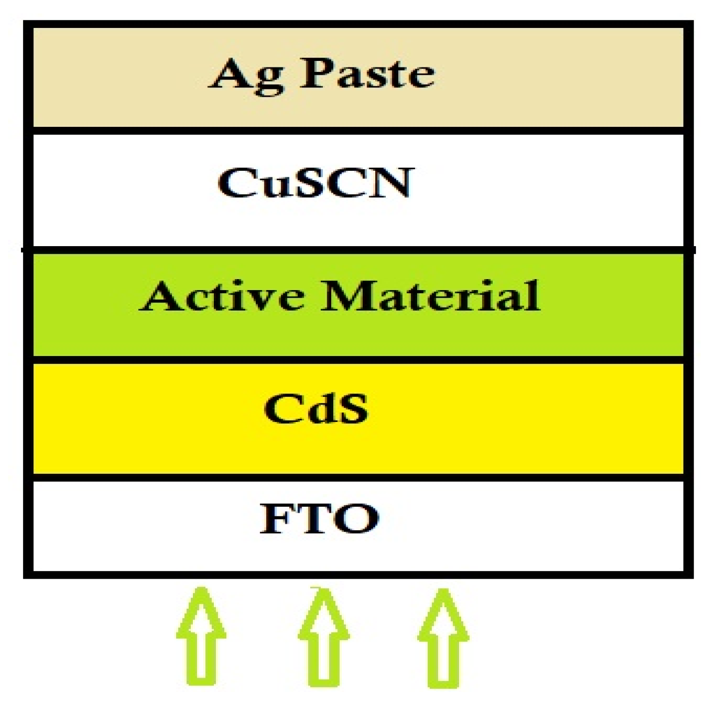
2. Device Architecture and Simulation

In our proposed FTO/CdS/Cs2TiI6−XBrX/CuSCN/Ag-based planar solar cell device model, the band gap of ETL (electron transport layer) materials, CdS and HTL material CuSCN are taken to be 2.4 eV, 3.26 eV and 3.4 eV, respectively, and the absorbing layer is tuneable under 1.0–1.78 eV [10,11,12,13,14,15]. The working temperature for the simulation is maintained at 27 °C with −0.8 V to 0.8 V bias voltage in the SCAPS-1D simulator. Here, Figure 1 shows the schematic view of the proposed structure. the simulation is carried out with illumination of AM 1.5 with the light power of 1000 W/m2 under Gaussian energy distribution, and its characteristic energy is set to 0.1 eV. With Br doping the lattice parameter, band structure and the optical properties of Cs2TiI6 can be changed. Thus, due to the doping effect, both Cs2TiI2Br4 and Cs2TiI3Br3 are suitable for solar cell applications. On the other side, based on the superior optical coincidence index and better absorption coefficient, Cs2TiI2Br4 and Cs2TiIBr5 are ideal for light harvesting applications [16]. The details of the device materials’ properties and active materials’ basic parameters taken for the work are shown in Table 1 and Table 2, respectively. The symbols, i.e., Eg, denote the band gap energy; ꭓ is the electron affinity; ℇr is the relative permittivity; NA is the acceptor density; ND is the donor density; Nt is the total defect density; NC is the conduction band effective density of states; NV is the valence band effective density of states, respectively. The default values of some parameters and settings are as follows: electron mobility is 4.4 cm2/Vs, hole mobility is 2.5 cm2/Vs and electron and hole thermal velocity is 107 cm/s [17]. The Shockley–Queisser limit of a perfect photovoltaic absorbing material is around 1.3 eV [16]. Our Cs2TiI6−XBrX-based active material has a band gap in the range of 1.07 to 1.78 eV which can be seen in Table 1.

3. Results and Discussion

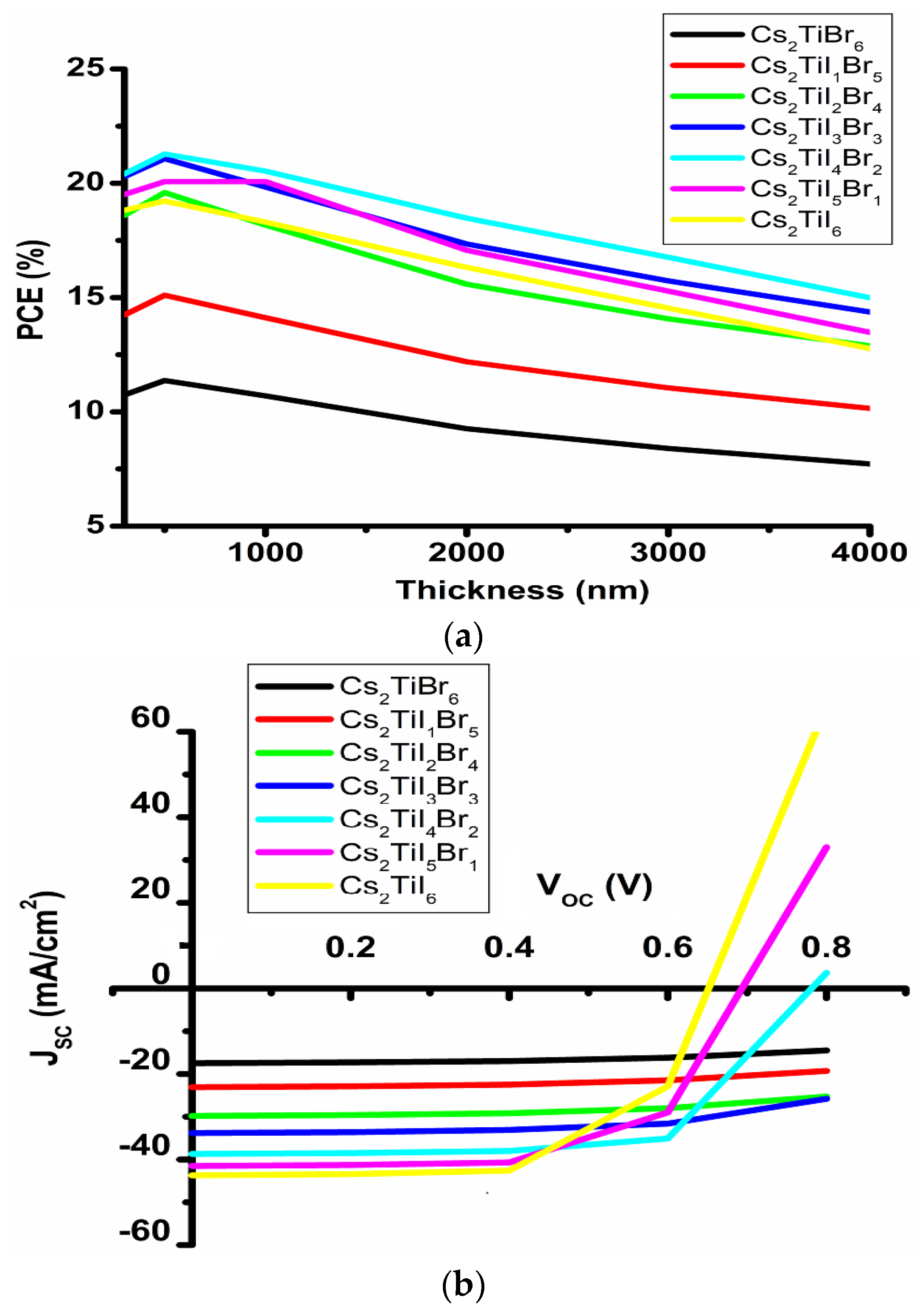
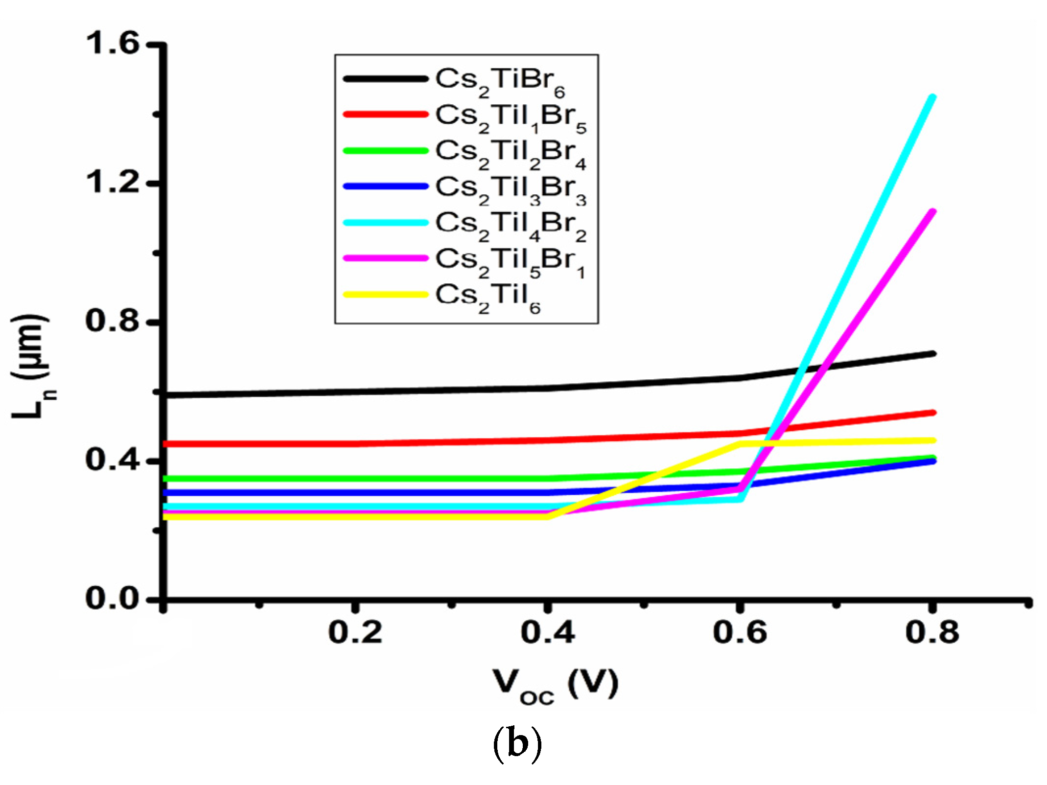
3.1. Optimization of Absorbing Layer Thickness with CdS Layer

In this section, the optimization of thickness of different perovskite absorbing layers such as Cs2TiBr6, Cs2TiI1Br5, Cs2TiI2Br4, Cs2TiI3Br3, Cs2TiI4Br2, Cs2TiI5Br1 and Cs2TiI6 has been studied at 27 °C temperature with standard defect density (~1014 cm−3) and a constant series resistance [18] by varying the thickness from 0.3 to 3.0 µm. Here, Figure 2a–c represent the PCE; a J-V graph with the thickness variation as 0.3 µm, 0.4 µm, 0.5 µm, 1.0 µm, 1.5 µm, 2.0 µm, 2.5 µm, 3.0 µm, 3.5 µm and 4.0 µm for the Cs2Ti–6−XBrX perovskite solar cell; and PCE with the back contacts’ metal work function. Generally, the lower thickness of absorbing material leads to a low absorption of sunlight, which has a direct impact on PCE. From Figure 2a,b, it is observed that after 0.5 µm thickness for the Cs2TiBr6, Cs2TiI1Br5, Cs2TiI2Br4, Cs2TiI3Br3 and Cs2TiI4Br2, and after 1.0 µm thickness for the Cs2TiI5Br1 and 0.4 µm thickness for the Cs2TiI6 absorbing layer, the PCE of the device cell starts to fall gradually. The reason behind this fall is due to the increment in thickness of the absorbing layer as the light absorption rate becomes much higher. Such excess light absorption leads to a temperature rise in the device, and thus VOC starts to fall drastically due to this temperature rise [12]. With the drop in VOC, the PCE of the device starts to decrease. We all are aware that the PCE is a key parameter to evaluate the total annual power generation of a perovskite solar cell device-based PV (photovoltaic) module. Thus, reducing the PCE will decrease the maximum generated power (PMAX) in the device. Despite the VOC starting to fall with thickness, the generation rate of the charge carrier increases, which has a direct impact on the enhancement of JSC [19]. Such an enhancement in JSC will increase the Shockley–Read–Hall (SRH) recombination [20,21]. This phenomenon could establish a VOC–JSC relationship in the PV module [20,21,22].
V OC   = nKT q ln   (   J SC   I 0   +   1 )
where T = device temperature, I0 = reverse saturation current, q = electronic charge, n = ideality factor and K = Boltzmann constant.
From Equation (1), it is shown that the VOC starts to fall as the reverse saturation current (I0) increases in the device. Therefore, by analyzing all the parameters we may conclude that the Cs2TiBr6, Cs2TiI1Br5, Cs2TiI2Br4, Cs2TiI3Br3 and Cs2TiI4Br2 materials are optimized at 0.5 µm; the Cs2TiI5Br1 material is optimized at 1.0 µm; and the Cs2TiI6 material is optimized at 0.4 µm.
From Figure 2c it is observed that the PCE increases with the higher metal work function of the Ag paste up to a certain work function value (5 eV). The reason behind such an increment in the work function value is the decrement of the height of the carrier barrier, and as a result, the metal contact becomes ohmic in nature [8]. Thus, open circuit voltages also increase.
On the other hand, Figure 3a,b indicate the changes in diffusion length (Ln) with the voltage variation at the ambient temperature (300 K). As per the observations, the diffusion length increases with the open circuit voltage (VOC) for all the seven absorbing materials except for Cs2TiI5Br1 and Cs2TiI6, where the diffusion length decreases after 0.6 V. The concentrations of electrons and holes are enhanced with the voltage which leads to an increment in diffusion length. The diffusion length of the electrons and holes should be higher than the absorbing layer thickness [8], since Cs2TiBr6, Cs2TiI1Br5 and Cs2TiI6 absorbing materials have a band gap above 1.50 eV which requires large energy to excite an electron in the conduction band. Thus, such materials operate in a higher temperature which can burn the device after a certain temperature. Therefore, despite the better power absorption and power generation capability of Cs2TiBr6, Cs2TiI1Br5 and Cs2TiI6 absorbing material, they are not suitable for PV application.

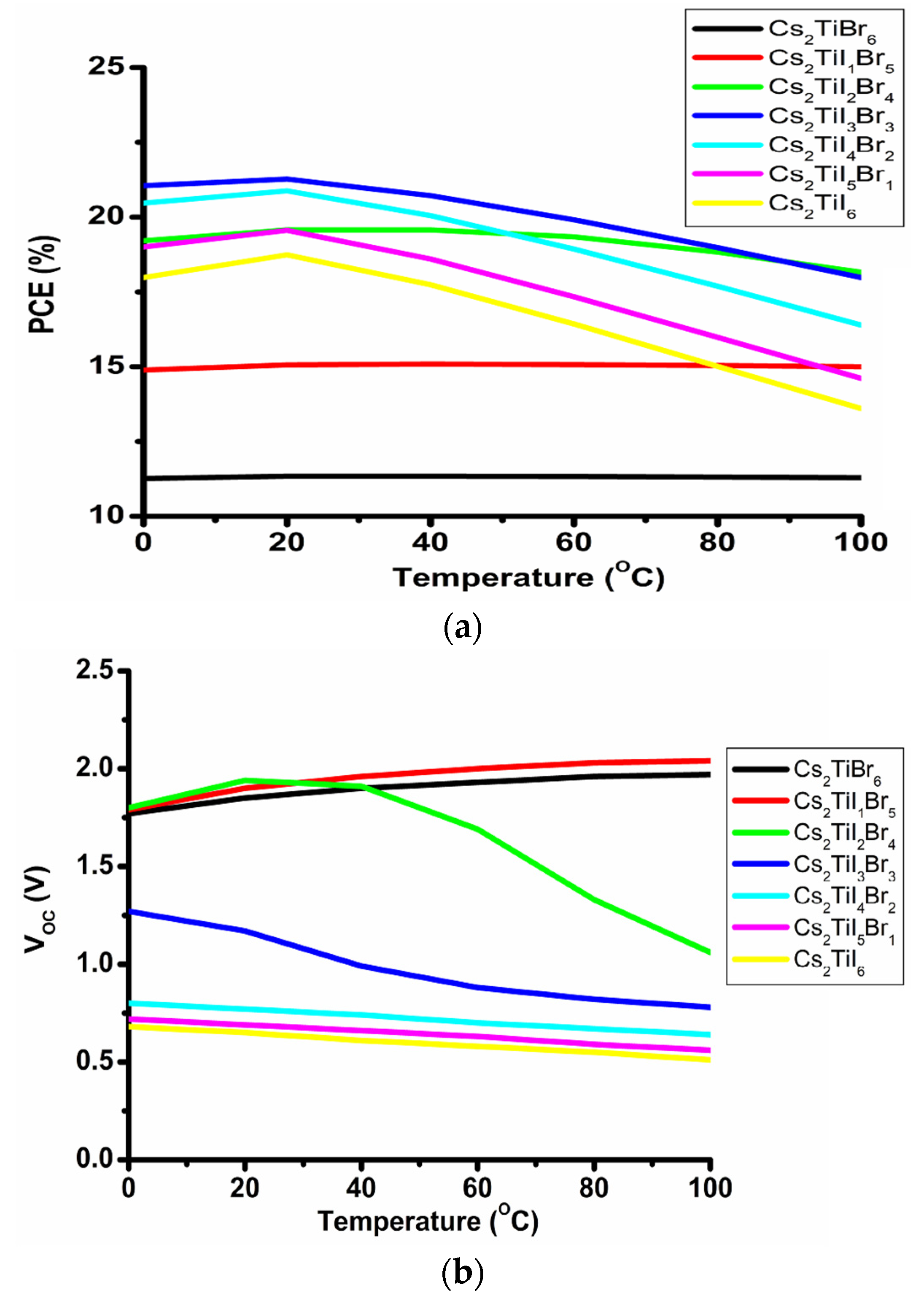
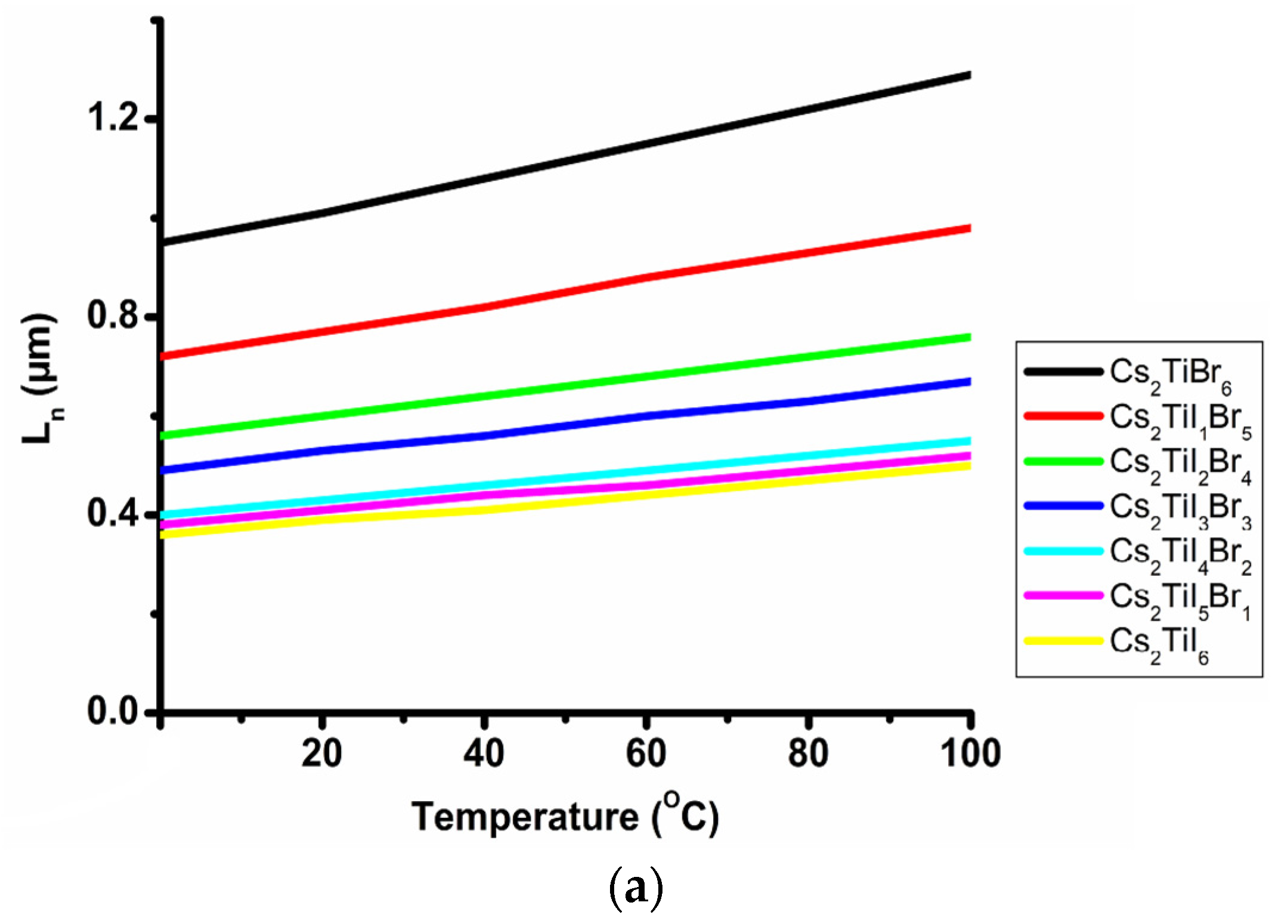
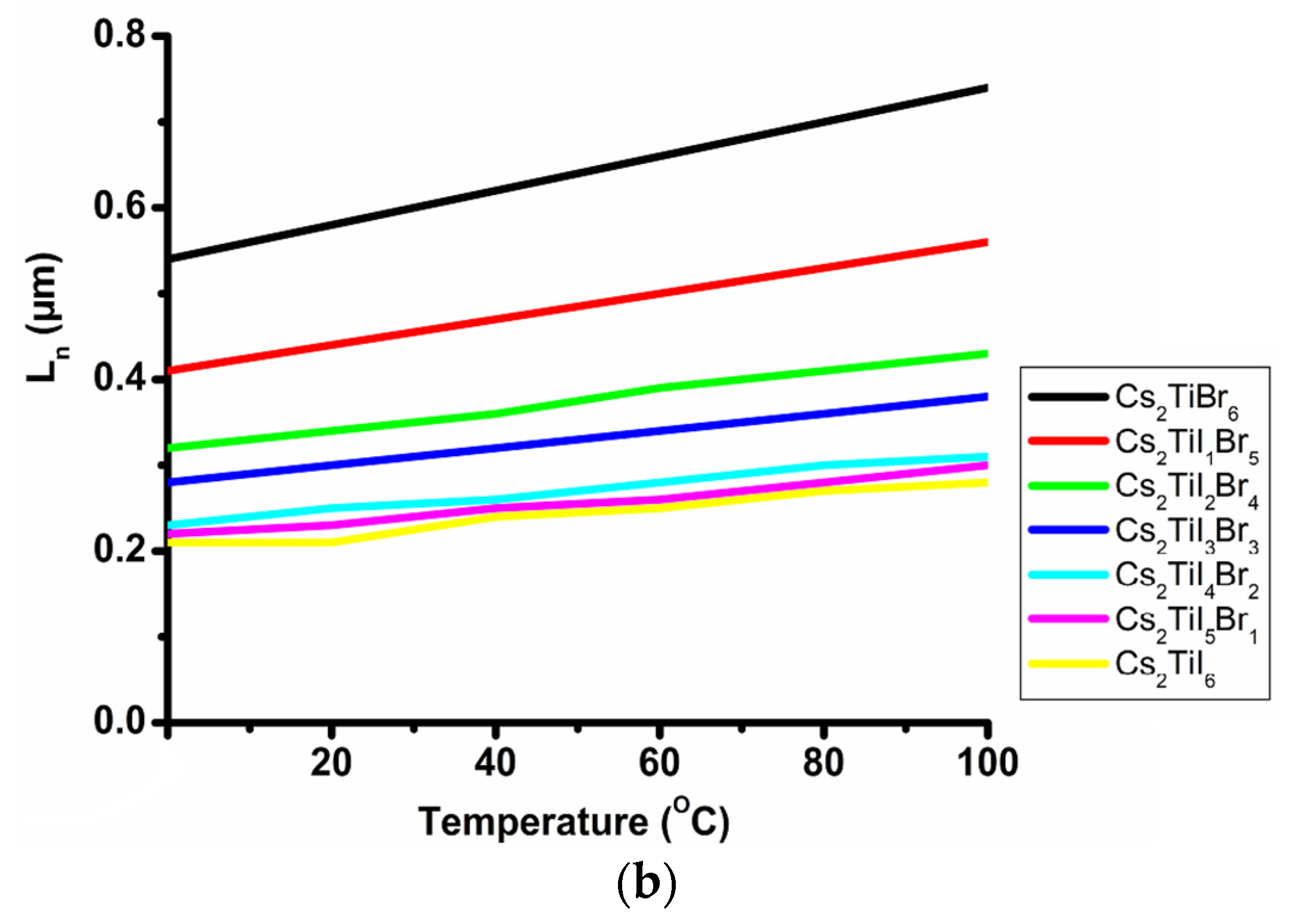
3.2. Optimization of Device Temperature with CdS Layer

In our study, we have varied the temperature from −10 °C (263 K) to 100 °C (373 K) at an optimized thickness (Cs2TiBr6 = 0.5 µm, Cs2TiI1Br5 = 0.5 µm, Cs2TiI2Br4 = 0.5 µm, Cs2TiI3Br3 = 0.5 µm, Cs2TiI4Br2 = 0.5 µm, Cs2TiI5Br1 = 1.0 µm and Cs2TiI6 = 0.4 µm) for the FTO/CdS/Cs2Ti–6−XBrX /CuSCN device structure. Here, Equation (1) can be rewritten as follows [23,24]:
V = K B T q   log   ( r if r 0 if )
where V = VOC, r if = I SC ,   r 0 if =   I 0 ,   n is the ideality factor, ISC is the short circuit current and I0 is the reverse saturation current.
From Equation (2) we can conclude that as the temperature starts to increase, the open circuit voltage (VOC) will decrease accordingly. The prime reason behind such a decrement in VOC is the exponential inverse increment in r0if in Equation (2), which leads to a similar exponential inverse increment in I0 due to the temperature rise [12]. On the other hand, the temperature increment may cause the increment in the recombination process which will lead to the increment in the short circuit current (ISC) [21]. Figure 4a,b show the changes in the PCE and VOC with the device temperature for the absorbing materials and suggest that up to 40 °C, the VOC increases quite significantly for the Cs2TiBr6, Cs2TiI1Br5 and Cs2TiI2Br4 absorbing material, and after that temperature there is a significant change observed in the VOC. Such a higher VOC starts to increase the PMAX. The reasons behind such peculiarities are the higher band gap of the Cs2TiBr6 (1.78 eV), Cs2TiI1Br5 (1.58 eV) and Cs2TiI2Br4 (1.38 eV) perovskite layers, and as the temperature starts to increase initially, the band gap of the materials starts to reduce, leading to a higher increment in the VOC for the Cs2TiBr6 (1.78 eV) and Cs2TiI1Br5 (1.58 eV) material. However, for the Cs2TiI2Br4 material after 40 °C, VOC starts to drop. On the other hand, Cs2TiI3Br3, Cs2TiI4Br2, Cs2TiI5Br1 and Cs2TiI6 materials have a lower band gap. So, when the temperature starts to rise, the open circuit voltage (VOC) starts to drop after 20 °C onwards despite the existence of almost constant JSC. As a result, PCE and PMAX after 20 °C start to reduce with the voltage drop. The same will be evidenced from Equation (2). This means as the temperature starts to rise, VOC starts to decrease continuously and the back recombination process is begun. As a result, the PCE starts to fall gradually. So, from the above analysis, we may conclude that the optimal temperature for the Cs2TiBr6, Cs2TiI1Br5 and Cs2TiI2Br4 materials is 40 °C and for the Cs2TiI3Br3, Cs2TiI4Br2, Cs2TiI5Br1 and Cs2TiI6 absorbing layers is 20 °C.
Similarly, changes in electron and hole diffusion length are depicted at 0 °C to 100 °C working temperature in Figure 5a,b. It can be observed that at a relatively higher temperature, the value of Ln is increasing simultaneously, as the diffusion length depends on the operating temperature and dopant concentration.

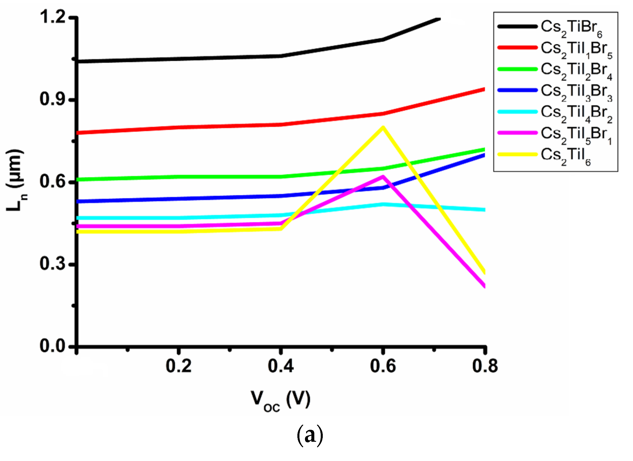
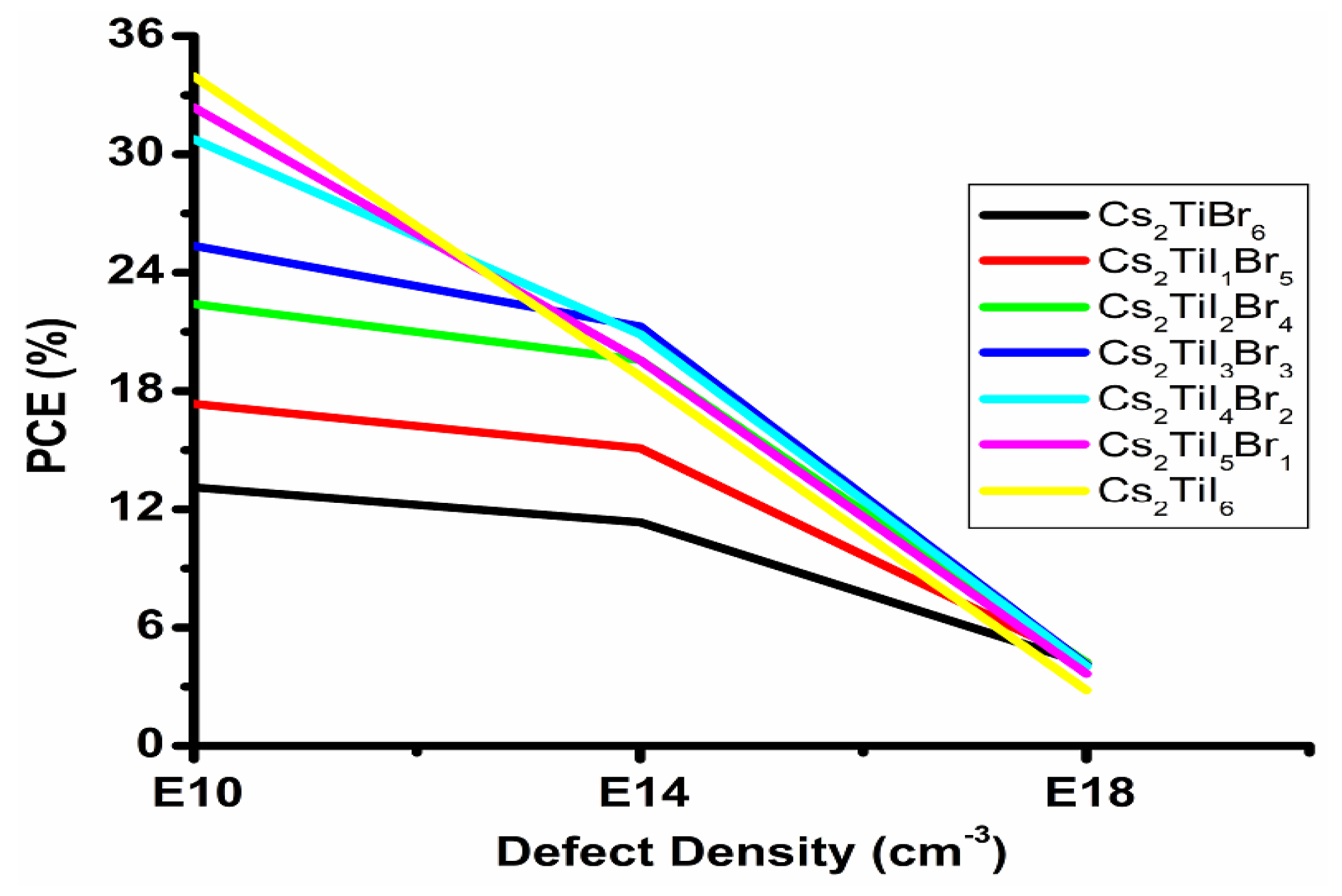
3.3. Optimization of Defect Density

The total defect density plays a key role in determining the performance of a perovskite solar cell device, as it can debase the performance quality of the device. It has caused heavy charge recombination between the interfaces [25]. In our present study, we have changed the total defect density (Nt, cm−3) from 1010 to 1020 in the perovskite absorbing layer with a cell architecture of FTO/CdS/Cs2Ti–6−XBrX/CuSCN to understand its effects on the device performances (PCE), and then tried to find out the optimum defect density for all the materials at the optimized thickness and temperature. It is observed that at a higher total defect density, there is a higher recombination of electron and hole pairs due to the generation of pinholes at the electrodes. Such a phenomenon reduces the stability of the device and overall performance of the device. The effects of defect density at the different interfaces are not included in this study. Here, Figure 6 shows the PCE variation with defect density for the Cs2Ti–6−XBrX absorbing layer with the CdS electron transport layer, respectively. So, from the above figures, it is clearly observed that the increment in defect density above 1010 cm−3 will reduce the PCE, respectively, for all the perovskite materials. We can also observe that for the Cs2TiBr6 absorbing material, the PCE decreases significantly with the defect density as it has a higher band gap as a result of the recombination rate starting to reduce. As a result, the collection of electron–hole pairs is also reduced and JSC starts to decrease. Such changes result in the reduction of VOC. The Cs2TiI1Br5, Cs2TiI2Br4, Cs2TiI3Br3, Cs2TiI4Br2, Cs2TiI5Br1 and Cs2TiI6 materials have a continuous VOC drop with JSC reduction, and as a result the PCE falls. This incident signifies that at the higher total defect density, the back recombination process increases due to the impurities’ enhancement in the absorbing materials, and as a result, conversion efficiency (PCE) loss starts to increase due to the VOC and JSC losses [24]. Such losses in the parameters will decrease the PMAX for the absorbing layers which can be observed in Figure 6. So, from the above analysis of the performance parameters, the optimal defect density for the C–2TiI6−XBrX absorbing layer with CdS ETL is 1010 cm−3. Hence, it can be concluded that the total defect density of the materials affects the PCE of the device as increasing defects imply reduction in the diffusion length of the electron and hole charge carriers.

4. Conclusions

This research article presents the optimization of the thickness of the absorbing layer with two different electron transport layers (CdS) numerically using the SCAPS simulator for the planar FTO/CdS/Cs2TiI6−XBrX /CuSCN structure. The results indicate the performance of the device (PCE, VOC) and maximum power conversion (PMAX) are better between 0.5 and 1 µm. Through further observations, we have seen that optimization of the device temperature lies between 10 °C and 60 °C and defect densities between 1010 and 1014 cm−3 for the different absorbing materials. During the simulation process, it was observed that defect densities have a great impact on the charge recombination rate. This research work has not covered the recombination rate in different interfaces of the solar cell device, which include the ETL/perovskite and perovskite/HTL interfaces.

Author Contributions

Conceptualization: K.C., N.R.M., K.D. and S.P.; methodology: K.C., S.D., N.R.M., K.D. and S.P.; software: K.C., S.L., W.E.-S., K.D. and N.F.S.; validation: W.E.-S., S.D., N.R.M. and S.L.; writing—original draft preparation: K.C., S.D., K.D. and N.F.S.; writing—review and editing: S.L., S.P., N.R.M. and W.E.-S.; supervision: S.P. and S.D.; project administration: W.E.-S.; funding acquisition: N.F.S. All authors have read and agreed to the published version of the manuscript.

Funding

This work is supported by Princess Nourah bint Abdulrahman University Researchers Supporting Project number (PNURSP2023R66), Princess Nourah bint Abdulrahman University, Riyadh, Saudi Arabia.

Institutional Review Board Statement

Not applicable.

Informed Consent Statement

Not applicable.

Data Availability Statement

The data presented in this research are available on request from the corresponding author.

Acknowledgments

The authors would like to acknowledge the Princess Nourah bint Abdulrahman University Researchers Supporting Project number (PNURSP2023R66), Princess Nourah bint Abdulrahman University, Riyadh, Saudi Arabia. The authors would like to acknowledge the support of Prince Sultan University for paying the Article Processing Charges (APC) of this publication.

Conflicts of Interest

The authors declare no conflict of interest.

References

  1. Kojima, A.; Teshima, K.; Shirai, Y.; Miyasaka, T. Organometal halide perovskites as visible-light sensitizers for photovoltaic cells. J. Am. Chem. Soc. 2009, 131, 6050–6051. [Google Scholar] [CrossRef] [PubMed]
  2. Giustino, F.; Snaith, H.J. Toward lead-free perovskite solar cells. ACS Energy Lett. 2016, 1, 1233–1240. [Google Scholar]
  3. Yang, W.S.; Noh, J.H.; Jeon, N.J.; Kim, Y.C.; Ryu, S.; Seo, J. High-performance photovoltaic perovskite layers fabricated through intramolecular exchange. Science 2015, 348, 1234–1237. [Google Scholar] [CrossRef] [PubMed]
  4. Yin, W.J.; Yang, J.H.; Kang, J.; Yan, Y.; Wei, S.H. Halide perovskite materials for solar cells: A theoretical review. J. Mater. Chem. A 2015, 3, 8926–8942. [Google Scholar] [CrossRef]
  5. Hosseini, S.R.; Bahramgour, M.; Sefidi, P.Y.; Mashayekh, A.T.; Moradi, A.; Delibas, N.; Hosseini, M.G.; Niaei, A. Investigating the effect of non-ideal conditions on the performance of a planar CH3NH3PbI3-based perovskite solar cell through SCAPS-1D simulation. Heliyon 2022, 8, e11471. [Google Scholar] [CrossRef] [PubMed]
  6. Ju, M.G.; Chen, M.; Zhou, Y.; Garces, H.F.; Dai, J.; Ma, L.; Padture, N.P.; Zeng, X.C. Earth- abundant non-toxic titanium (IV) based vacancy-ordered double perovskite halides with tunable 1.0 to 1.8 eV bandgaps for photovoltaic applications. ACS Energy Lett. 2018, 3, 297–304. [Google Scholar] [CrossRef]
  7. Chen, M.; Ju, M.G.; Carl, A.D.; Zong, Y.; Grimm, R.L.; Gu, J.; Zeng, X.C.; Zhou, Y.; Padture, N.P. Cesium Titanium (IV) Bromide thin Films based stable lead-free perovskite solar cells. Joule 2018, 23, 558–570. [Google Scholar] [CrossRef]
  8. Shyma, A.P.; Sellappan, R. Computational Probing of Tin-Based Lead-Free Perovskite Solar Cells: Effects of Absorber Parameters and Various Electron Transport Layer Materials on Device Performance. Materials 2022, 15, 7859. [Google Scholar]
  9. Omarova, Z.; Yerezhep, D.; Aldiyarov, A.; Tokmoldin, N. In Silico Investigation of the Impact of Hole-Transport Layers on the Performance of CH3NH3SnI3 Perovskite Photovoltaic Cells. Crystals 2022, 12, 699. [Google Scholar] [CrossRef]
  10. Umar, A.; Tiwari, P.; Srivastava, V.; Lohia, P.; Dwivedi, D.K.; Qasem, H.; Akbar, S.; Algadi, H.; Baskoutas, S. Modeling and Simulation of Tin Sulfide (SnS)-Based Solar Cell Using ZnO as Transparent Conductive Oxide (TCO) and NiO as Hole Transport Layer (HTL). Micromachines 2022, 13, 2073. [Google Scholar] [CrossRef]
  11. Ke, W.; Kanatzidis, G.M. Prospects for low-toxicity lead-free perovskite solar cells. Nat. Commun. 2019, 10, 965. [Google Scholar] [CrossRef]
  12. Chaudhary, N.; Chaudhary, R.; Kesari, J.P.; Patra, A.; Chand, S. Copper thiocyanate (CuSCN): An efficiency solution processable hole transporting layer in organic solar cells. J. Mater. Chem. C 2015, 3, 11886–11892. [Google Scholar] [CrossRef] [Green Version]
  13. Yang, Y.; You, J. Make perovskite solar cell stable. Nature 2017, 544, 155–156. [Google Scholar] [CrossRef]
  14. Bishnoi, S.; Pandey, S.K. Device performance analysis for lead-free perovskite solar cell optimization. IET Optoelect. 2018, 12, 185–190. [Google Scholar] [CrossRef]
  15. Chakraborty, K.; Choudhury, M.G.; Paul, S. Numerical study of Cs2TiX6(X=Br, I, F and Cl) based perovskite solar cell using SCAPS-1D device simulation. Solar Energy 2019, 194, 886–892. [Google Scholar] [CrossRef]
  16. Sheng, S.-Y.; Zhao, Y.-Y. First-principles study on the electronic and optical properties of strain-tuned mixed-halide double perovskites Cs2TiI6−XBrX. Phys. B Condens. Matter 2022, 626, 413522. [Google Scholar] [CrossRef]
  17. Chakraborty, K.; Choudhury, M.G.; Paul, S. Study of Physical, Optical and Electrical Properties of Cesium Titanium (IV) Based Single Halide Perovskite Solar Cell. IEEE J. Photovolt. 2021, 11, 386–390. [Google Scholar] [CrossRef]
  18. Li, C.; Luo, H.; Gu, H.; Li, H. BTO-Coupled CIGS Solar Cells with High Performances. Materials 2022, 15, 5883. [Google Scholar] [CrossRef] [PubMed]
  19. Heriche, H.; Rouabah, Z.; Bouarissa, N. New ultra-thin CIGS structure solar cells using SCAPS simulation program. Int. J. Hydrog. Energy 2017, 42, 9524–9532. [Google Scholar] [CrossRef]
  20. Mostefaoui, M.; Mazar, H.; Khelifi, S. Simulation of high efficiency CIGS solar cells with SCAPS-1D software. Energy Procedia 2015, 74, 736–744. [Google Scholar] [CrossRef]
  21. Pandey, R.; Chaujar, R. Numerical simulations: Toward the design of 27.6% efficient four-terminal semi-transparent perovskite/Sic passivated rear contact silicon tandem solar cell. Superlattices Microstruct. 2016, 100, 656–666. [Google Scholar] [CrossRef]
  22. Paul, S.; Grover, S.; Repins, I.L.; Keyes, B.M.; Contreras, M.A.; Ramanathan, K.; Noufi, R.; Zhao, Z.; Liao, F.; Li, J.V. Analysis of back-contact interface recombination in thin-film solar cells. IEEE J. Photovolt. 2018, 8, 871–878. [Google Scholar] [CrossRef]
  23. Rahul; Singh, P.K.; Singh, R.; Singh, V.; Bhattacharya, B.; Khan, Z.H. New class of lead-free perovskite material for low-cost solar cell application. Mater. Res. Bull. 2018, 97, 572–577. [Google Scholar] [CrossRef]
  24. Adewoyin, A.D.; Olopade, M.A.; Oyebola, O.O.; Chendo, M.A. Development of CZTGS/CZTS tandem thin film solar cell using SCAPS-1D. Optik 2019, 176, 132–142. [Google Scholar] [CrossRef]
  25. Wang, X.; Zhang, T.; Lou, Y.; Zhao, Y. All inorganic lead-free perovskite for optoelectronic applications. Mater. Chem. 2019, 3, 365–375. [Google Scholar] [CrossRef]
Figure 1. Schematic view of the proposed solar cell structure.
Micromachines 14 00447 g001
Figure 2. Performance of Cs2Ti–6−XBrX absorbing layer with thickness variation for FTO/CdS/Cs2Ti–6−XBrX/CuSCN/Ag structure: (a) PCE, (b) J-V plot and (c) electrical properties of metal work function.
Micromachines 14 00447 g002aMicromachines 14 00447 g002b
Figure 3. Changes in diffusion length with the open circuit voltage: (a) electron, (b) hole.
Micromachines 14 00447 g003aMicromachines 14 00447 g003b
Figure 4. Device performance of Cs2Ti–6−XBrX absorbing layer for the CdS ETL with temperature variation at optimized thickness: (a) PCE, (b) VOC.
Micromachines 14 00447 g004
Figure 5. Changes in diffusion length with the working temperature: (a) electron, (b) hole.
Micromachines 14 00447 g005aMicromachines 14 00447 g005b
Figure 6. PCE of C–2TiI6−XBrX absorbing layer with different defect densities at optimized thickness and temperature for CdS ETL.
Micromachines 14 00447 g006
Table 1. Device material properties.
PropertiesCuSCNCdSFTO
Thickness (µm)0.350.500.1
Eg (eV)3.402.403.60
Ea (eV)1.904.184.0
r9.010.09.0
ND (1/cm3)01 × 10152.4 × 1018
NA (1/cm3)1 × 101801 × 105
µn (cm2/VS)2 × 10−4100100
µp (cm2/VS)1 × 10−22525
Table 2. Basic parameters’ properties.
PropertiesCs2TiI1Br5Cs2TiI2Br4Cs2TiI3Br3Cs2TiI4Br2Cs2TiI5Br1Cs2TiBr6Cs2TiI6
Thickness (µm)0.3–40.3–40.3–40.3–40.3–40.3–40.3–4
Band gap, Eg (eV)1.581.381.261.151.071.781.65
Electron affinity, Ea (eV)3.423.623.743.853.934.474.20
Relative permittivity, ℇr10192225281018
Donor density, ND (1/cm3)1 × 10192 × 10191 × 10185 × 10185 × 10181 × 10199 × 1018
Acceptor density, NA (1/cm3)1 × 10192 × 10191 × 10185 × 10185 × 10181 × 10199 × 1018
Electron mobility, µn (cm2/VS)4.45.45.87.87.84.48.4
Hole mobility, µp (cm2/VS)2.52.93.13.93.92.54.3
Disclaimer/Publisher’s Note: The statements, opinions and data contained in all publications are solely those of the individual author(s) and contributor(s) and not of MDPI and/or the editor(s). MDPI and/or the editor(s) disclaim responsibility for any injury to people or property resulting from any ideas, methods, instructions or products referred to in the content.

