
A Delay-Cell-Controlled VCO Design for Unipolar Single-Gate Enhancement-Mode TFT Technologies

Abstract
:1. Introduction
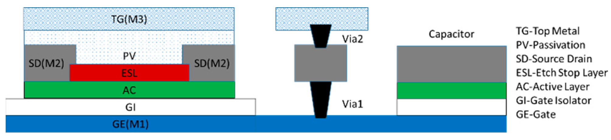
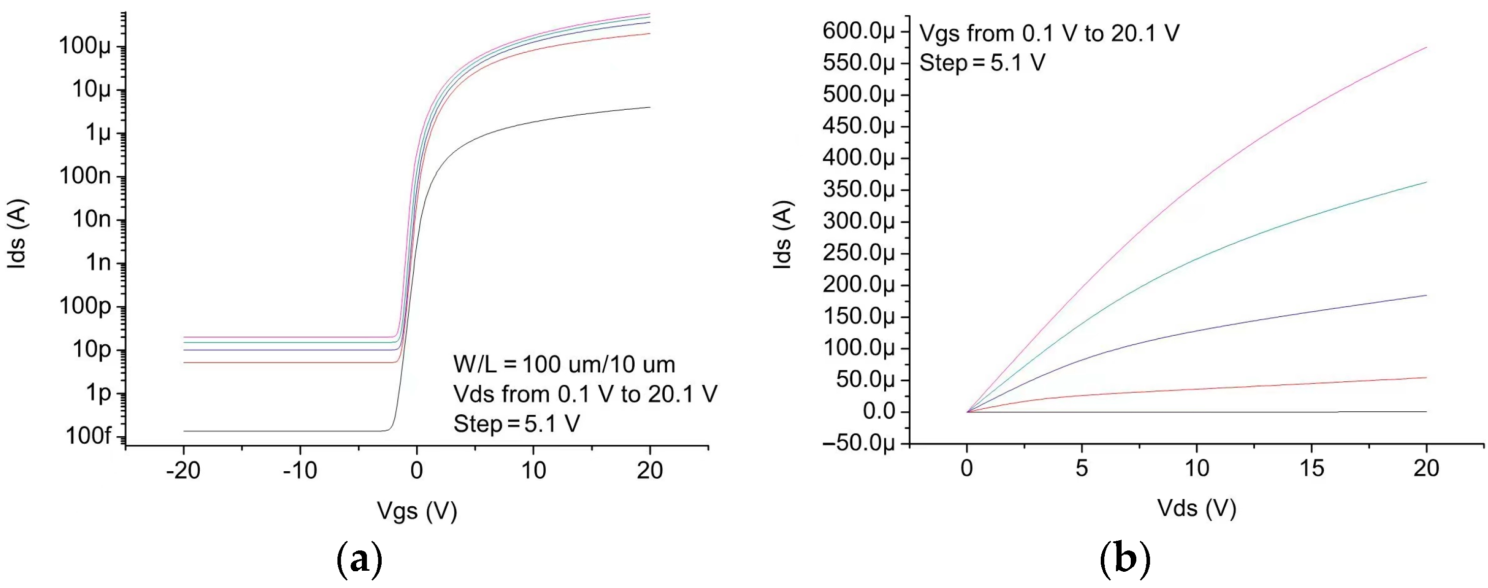
2. Device
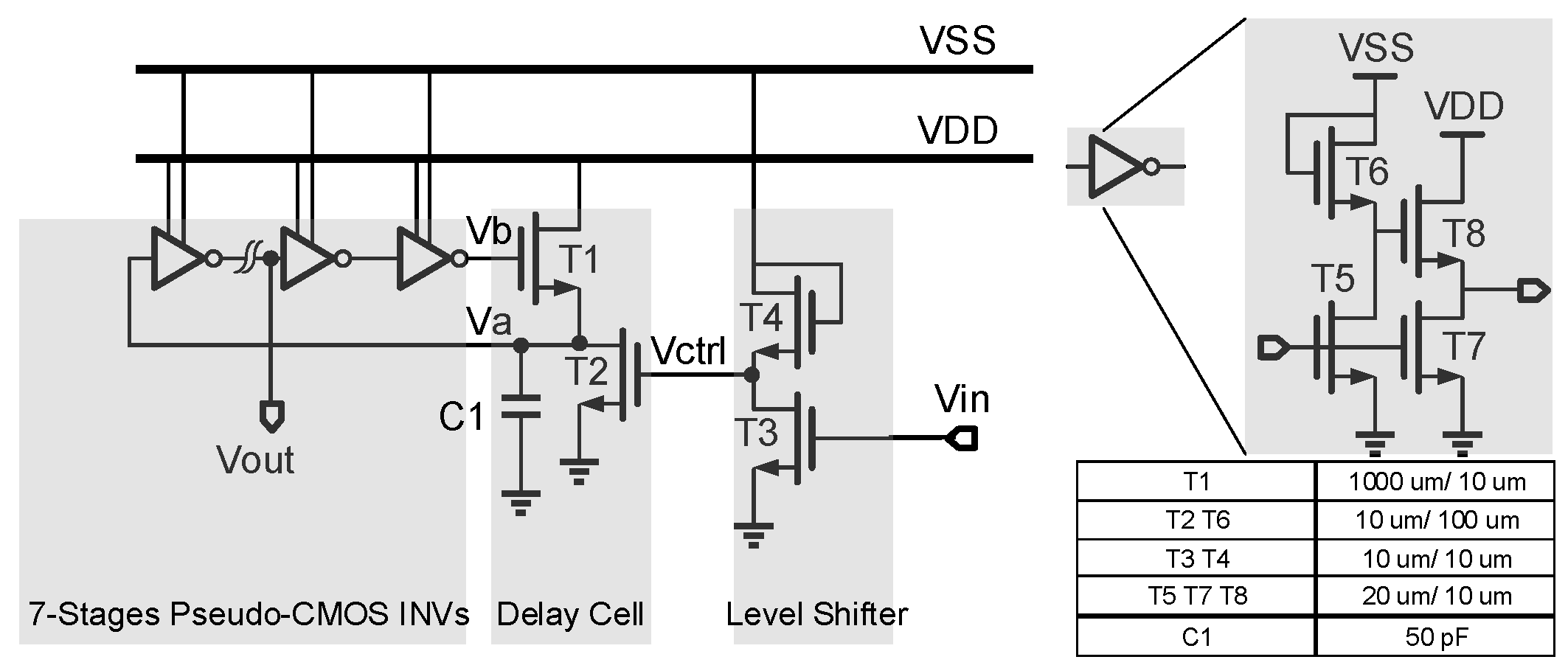
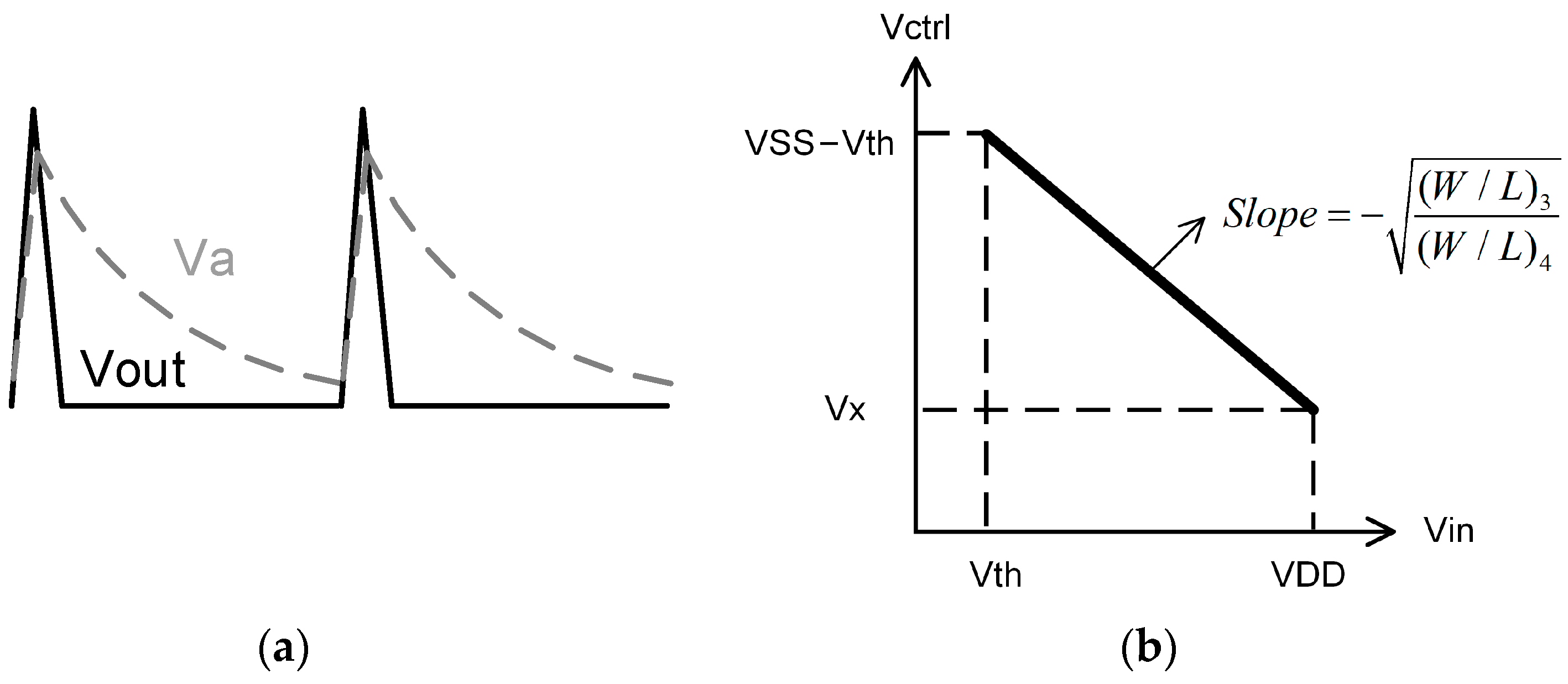
3. Circuit Design
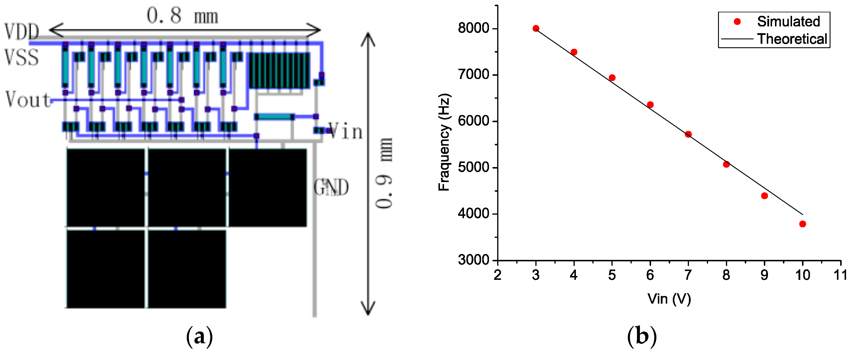
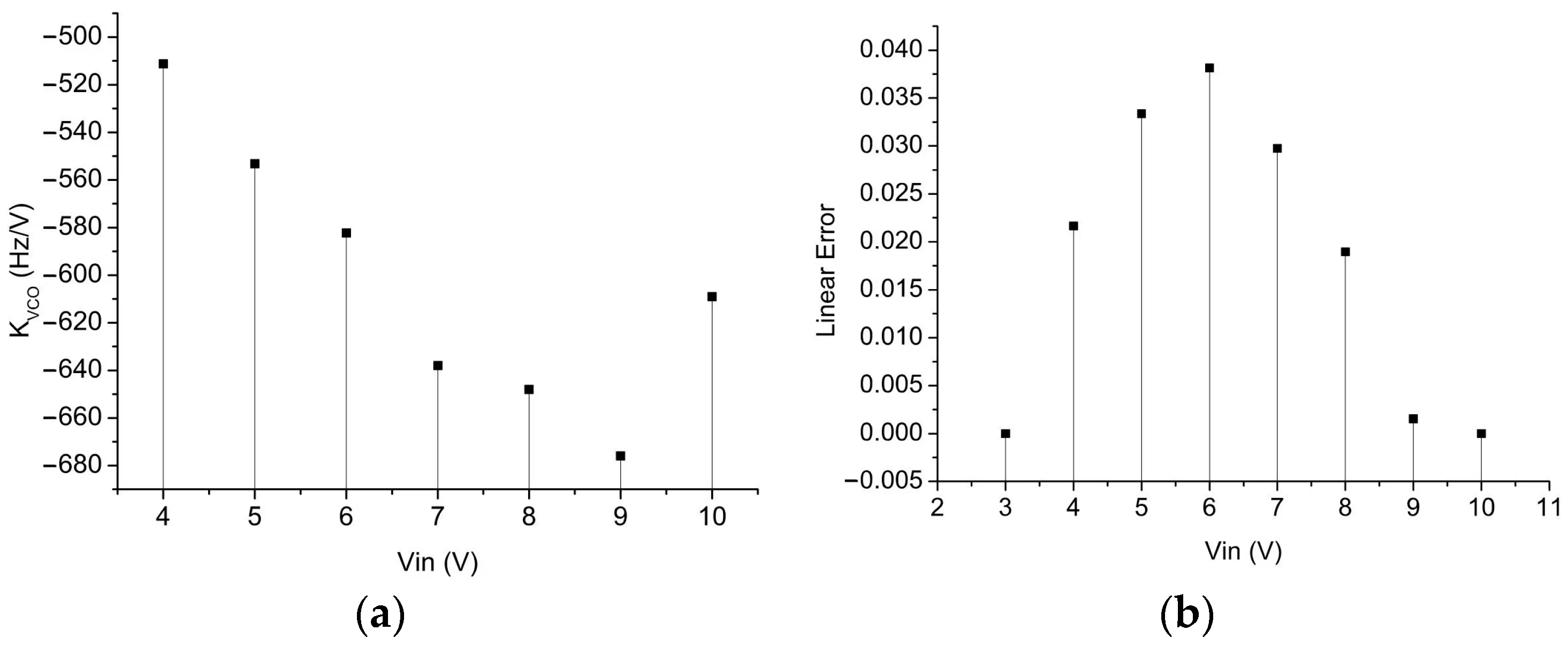
4. Simulation Results and Discussion
5. Conclusions
Author Contributions
Funding
Institutional Review Board Statement
Informed Consent Statement
Data Availability Statement
Conflicts of Interest
References
- Biggs, J.; Myers, J.; Kufel, J.; Ozer, E.; Craske, S.; Sou, A.; Ramsdale, C.; Williamson, K.; Price, R.; White, S. A natively flexible 32-bit arm microprocessor. Nature 2021, 595, 532–536. [Google Scholar] [CrossRef] [PubMed]
- Zulqarnain, M.; Stanzione, S.; Rathinavel, G.; Smout, S.; Willegems, M.; Myny, K.; Cantatore, E. A flexible ECG patch compatible with NFC RF communication. NPJ Flex. Electron. 2020, 4, 1–8. [Google Scholar] [CrossRef]
- Meister, T.; Ishida, K.; Carta, C.; Munzenrieder, N.; Ellinger, F. Flexible Electronics for Wireless Communication: A Technology and Circuit Design Review with an Application Example. IEEE Microw. Mag. 2022, 23, 24–44. [Google Scholar] [CrossRef]
- Ramkumar, G.; Jürgen, K.; Klaus, L.; Glesner, M. Investigation of voltage-controlled oscillator circuits using organic thin-film transistors (OTFT) for use in VCO-based analog-to-digital converters. Solid-State Electron. 2014, 93, 8–14. [Google Scholar]
- Sun, W.Y.; Zhao, Q.H.; Qiao, F.; Liu, Y.; Yang, H.; Guo, X.; Zhou, L.; Wang, L. An 8b 0.8kS/s configurable VCO-based ADC using oxide TFTs with Inkjet printing interconnection. In Proceedings of the 2017 IEEE International Symposium on Circuits and Systems (ISCAS), Baltimore, MD, USA, 28–31 May 2017. [Google Scholar]
- Raiteri, D.; van Lieshout, P.; van Roermund, A.; Cantatore, E. An Organic VCO-Based ADC for Quasi-Static Signals Achieving 1LSB INL at 6b Resolution. In Proceedings of the IEEE International Solid-State Circuits Flagship Conference of the IEEE Solid-State-Circuits-Society (ISSCC), San Francisco, CA, USA, 17–21 February 2013. [Google Scholar]
- Li, H.; Deng, S.; Xu, Y.; Zhong, W.; Luo, D.; Li, G.; Kwok, H.S.; Chen, R. A Differential Ring Oscillator with Tail Current Source Control Scheme Using N-Type Oxide TFTs. IEEE Trans. Electron Devices 2022, 69, 1870–1875. [Google Scholar] [CrossRef]
- Xu, Y.; Zhong, W.; Li, B.; Deng, S.; Fan, H.; Wu, Z.; Lu, L.; Yeung, F.S.Y.; Kwok, H.S.; Chen, R. An Integrator and Schmitt Trigger Based Voltage-to-Frequency Converter Using Unipolar Metal-Oxide Thin Film Transistors. IEEE J. Electron Devices Soc. 2021, 9, 144–150. [Google Scholar] [CrossRef]
- Keragodu, T.; Tiwari, B.; Bahubalindruni, P.; Goes, J.; Barquinha, P. A Voltage Controlled Oscillator Using IGZO Thin-Film Transistors. In Proceedings of the 2018 IEEE International Symposium on Circuits and Systems (ISCAS), Florence, Italy, 27–30 May 2018. [Google Scholar]
- Meister, T.; Ishida, K.; Knobelspies, S.; Cantarella, G.; Münzenrieder, N.; Tröster, G.; Carta, C.; Ellinger, F. 5–31-Hz 188-μW Light-Sensing Oscillator with Two Active Inductors Fully Integrated on Plastic. IEEE J. Solid-State Circuits 2019, 54, 2195–2206. [Google Scholar] [CrossRef]
- Lin, Y.-Z.; Liu, C.; Zhang, J.-H.; Yuan, Y.-K.; Cai, W.; Zhou, L.; Xu, M.; Wang, L.; Wu, W.-J.; Peng, J.-B. Active-Matrix Micro-LED Display Driven by Metal Oxide TFTs Using Digital PWM Method. IEEE Trans. Electron. Devices 2021, 68, 5656–5661. [Google Scholar] [CrossRef]
- Huang, T.-C.; Fukuda, K.; Lo, C.-M.; Yeh, Y.-H.; Sekitani, T.; Someya, T.; Cheng, K.-T. Pseudo-CMOS: A design style for low-cost and robust flexible electronics. IEEE Trans. Electron. Devices 2011, 58, 141–150. [Google Scholar] [CrossRef]


| Simplified Schematic | Input Impedance | Output Waveform | |
|---|---|---|---|
| Digital RO with VDD control [4,5] |  | Low | Digital square wave |
| Digital RO with delay-cell-control [6] |  | High | Digital pulse |
| Analog RO with tail-current source-control [7] |  | High | Analog sinewave |
| Bistable oscillator [8] |  | Moderate 2 | Digital pulse |
| Relaxation oscillator [9] |  | Low | Digital square wave |
| LC oscillator [10] 1 |  | High | Analog sinewave |
| [4] | [5] 1,2 | [6] 2 | [7] | [8] 1 | [9] 1 | This Work 1 | |
|---|---|---|---|---|---|---|---|
| TFT type | Organic unipolar single-gate enhancement | Oxide unipolar single-gate enhancement | Organic unipolar dual-gate depletion | Oxide unipolar single-gate enhancement | Oxide unipolar single-gate enhancement | Oxide unipolar single-gate enhancement | Oxide unipolar single-gate enhancement |
| VCO architecture | Digital RO with VDD control | Digital RO with VDD Control | Digital RO with delay-cell-control | Analog RO with tail-current source-control | Bi-stable oscillator | Relaxation oscillator | Digital RO with delay-cell-control |
| Supply (V) | −20–−15 | 6–14 | 20 | 15 | VDD = 6 V VSS = 8 V | ±5 | VDD = 10 V VSS = 20 V |
| Power (μW) | 150–450 3 | 100–1000 3 | 6 | 1500 | 109 | 1300 | 500 |
| Area (mm2) | - | 0.3 3 | 1 3 | 3.37 | - | - | 0.7 |
| Output frequency range (Hz) | 1.3 k–2.1 k 3 | 100 k–200 k 3 | 4—38 | 111 k–171 k | 1 k–2 k | 400–550 3 | 3.8 k–8 k |
| Input voltage range (V) | −20–−15 | 6–14 | 0–20 | 2–15 | 1–2 | −5– +5 | 3–10 |
| Average tuning sensitivity (Hz/V) | 160 | 12.5 k | 1.7 | 4.6 k | 1 k | 15 | 600 |
| Max linear error | 0.011 3 | 0.01–0.13 3 | 0.016 | 0.04 | 0.016 | Large | 0.04 |
Disclaimer/Publisher’s Note: The statements, opinions and data contained in all publications are solely those of the individual author(s) and contributor(s) and not of MDPI and/or the editor(s). MDPI and/or the editor(s) disclaim responsibility for any injury to people or property resulting from any ideas, methods, instructions or products referred to in the content. |
© 2022 by the authors. Licensee MDPI, Basel, Switzerland. This article is an open access article distributed under the terms and conditions of the Creative Commons Attribution (CC BY) license (https://creativecommons.org/licenses/by/4.0/).
Share and Cite
Li, B.; Wei, S.; Zhao, M.; Chen, R.; Wu, Z.; Xu, Y. A Delay-Cell-Controlled VCO Design for Unipolar Single-Gate Enhancement-Mode TFT Technologies. Micromachines 2023, 14, 32. https://doi.org/10.3390/mi14010032
Li B, Wei S, Zhao M, Chen R, Wu Z, Xu Y. A Delay-Cell-Controlled VCO Design for Unipolar Single-Gate Enhancement-Mode TFT Technologies. Micromachines. 2023; 14(1):32. https://doi.org/10.3390/mi14010032
Chicago/Turabian StyleLi, Bin, Siwei Wei, Mingjian Zhao, Rongsheng Chen, Zhaohui Wu, and Yuming Xu. 2023. "A Delay-Cell-Controlled VCO Design for Unipolar Single-Gate Enhancement-Mode TFT Technologies" Micromachines 14, no. 1: 32. https://doi.org/10.3390/mi14010032