
A Review of Various Attempts on Multi-Functional Encapsulation Technologies for the Reliability of OLEDs

Abstract
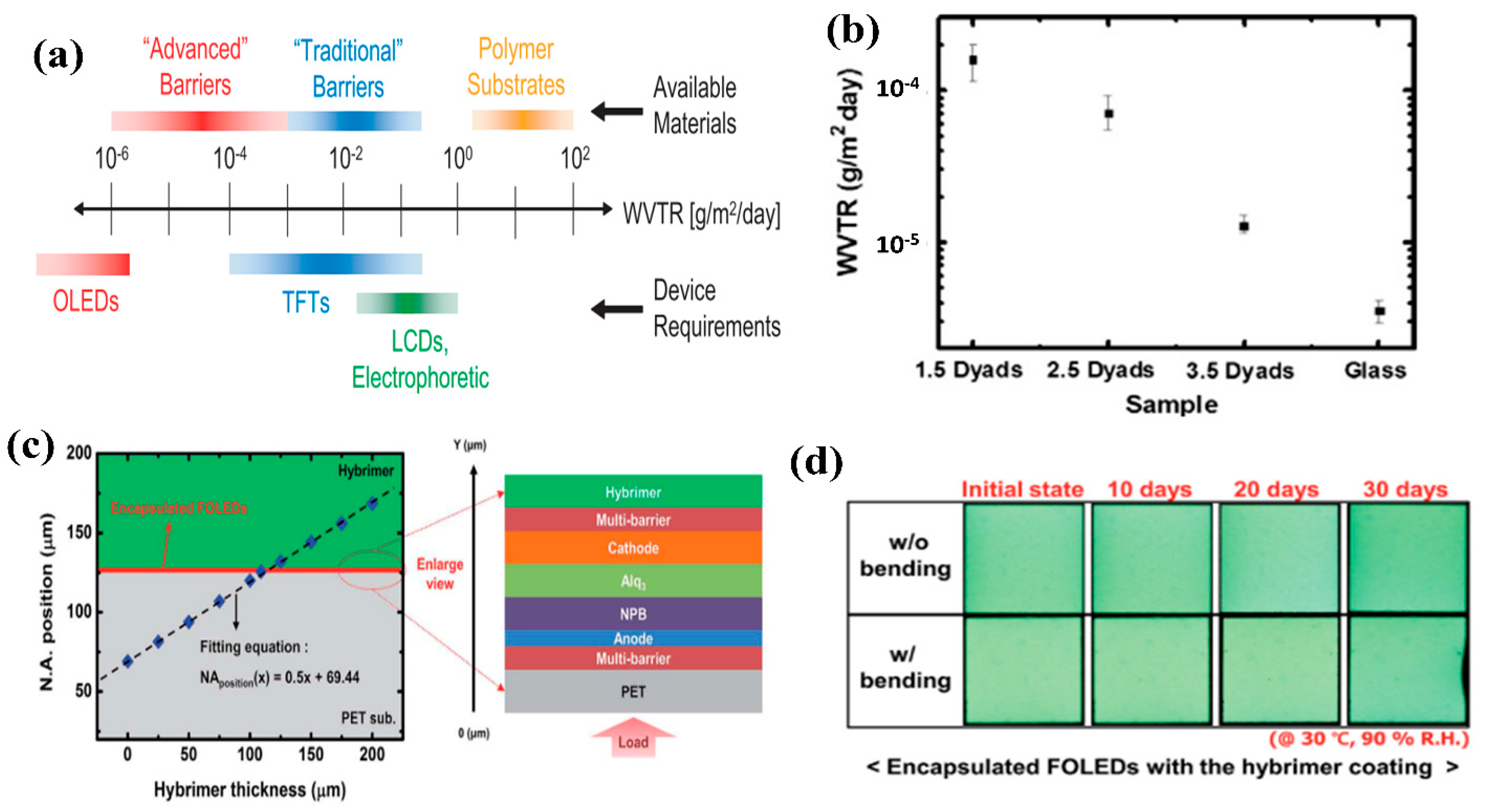
:1. Introduction
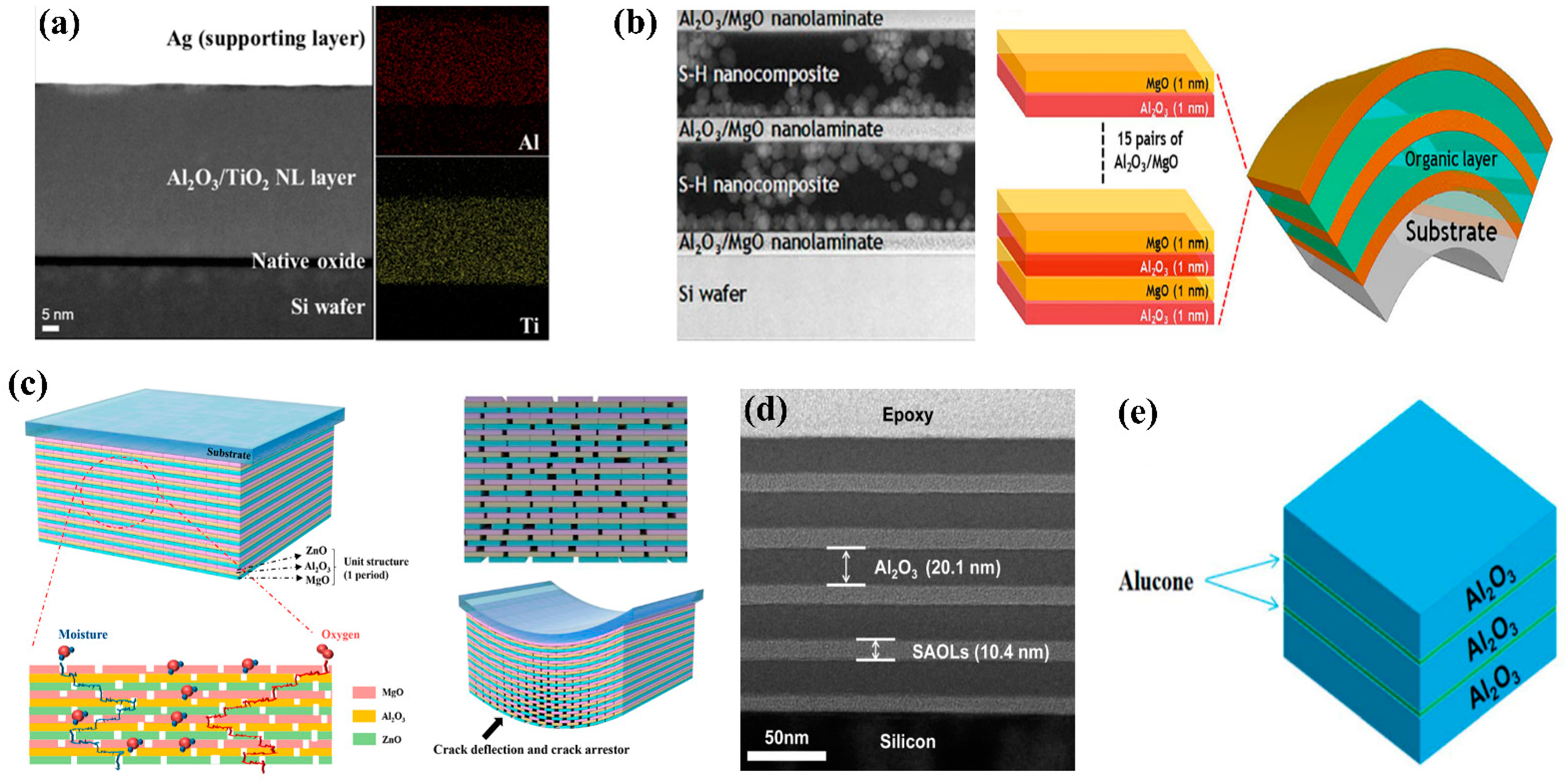
2. Highly Impermeable and Flexible TFE Using Stress-Robust Techniques
3. Various Functional TFE Technologies for the Reliability of OLEDs
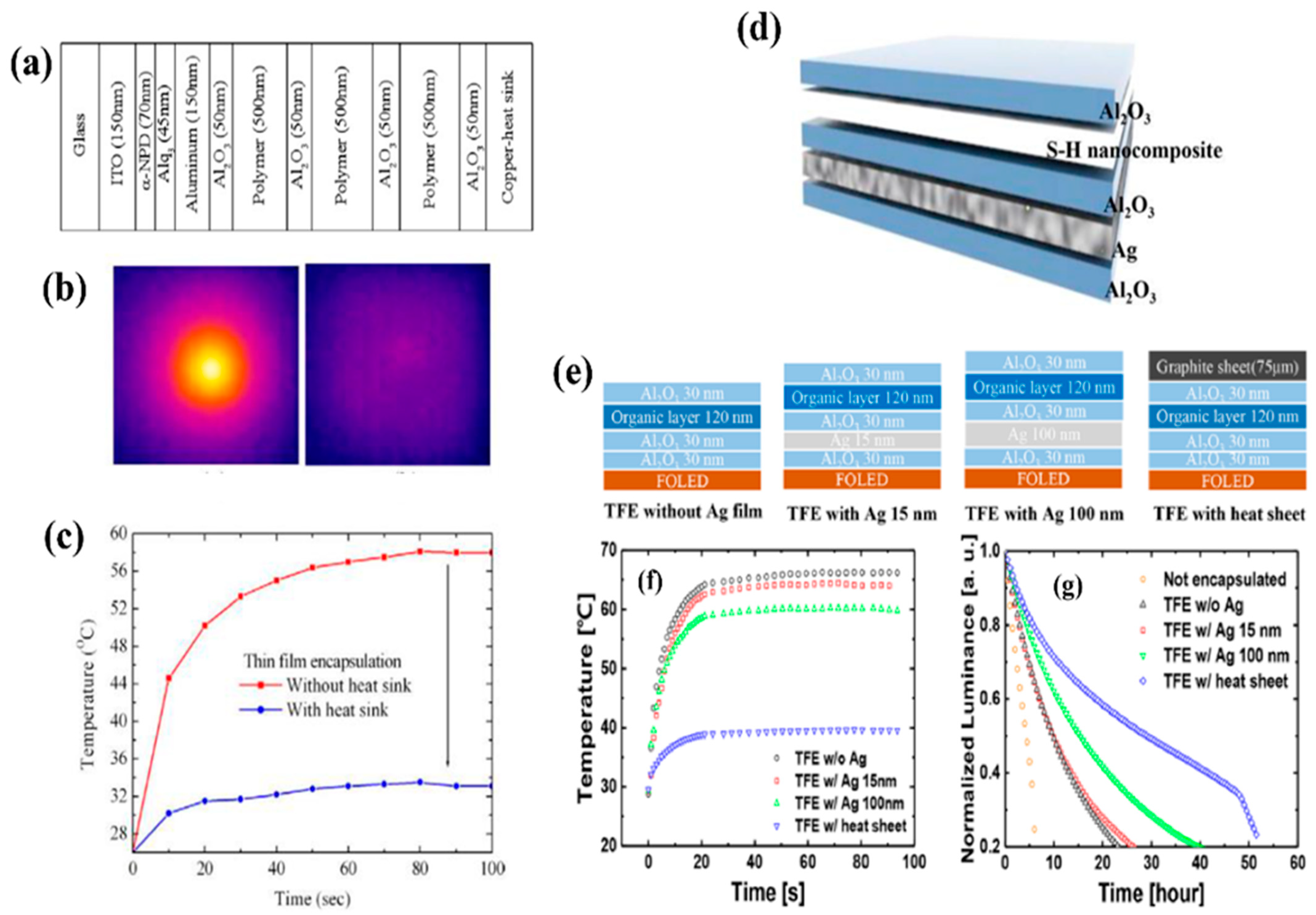
3.1. Heat-Transferable TFE Inserted with Thermally Conductive Films
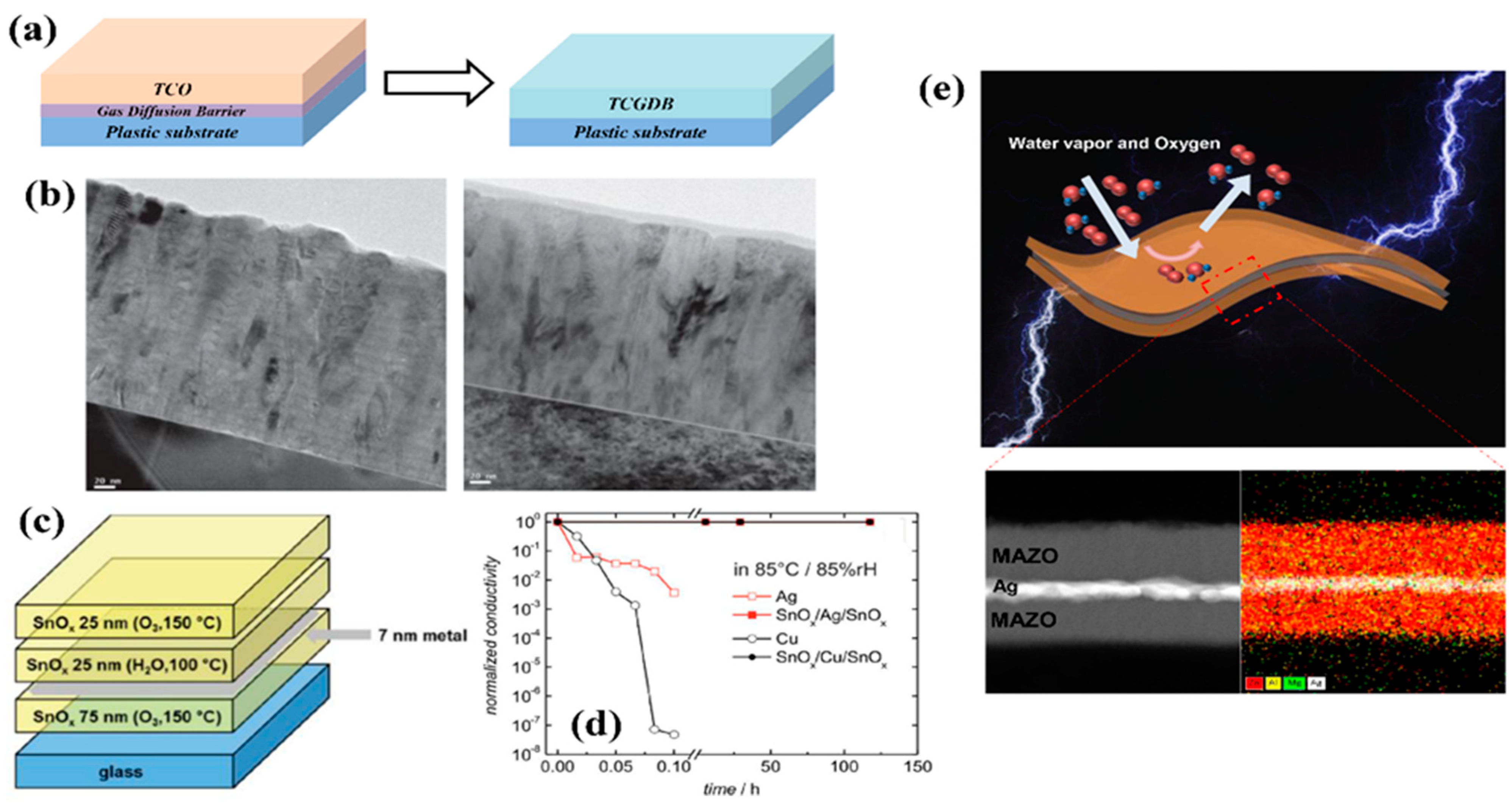
3.2. Transparent Conductive Gas Diffusion Barrier
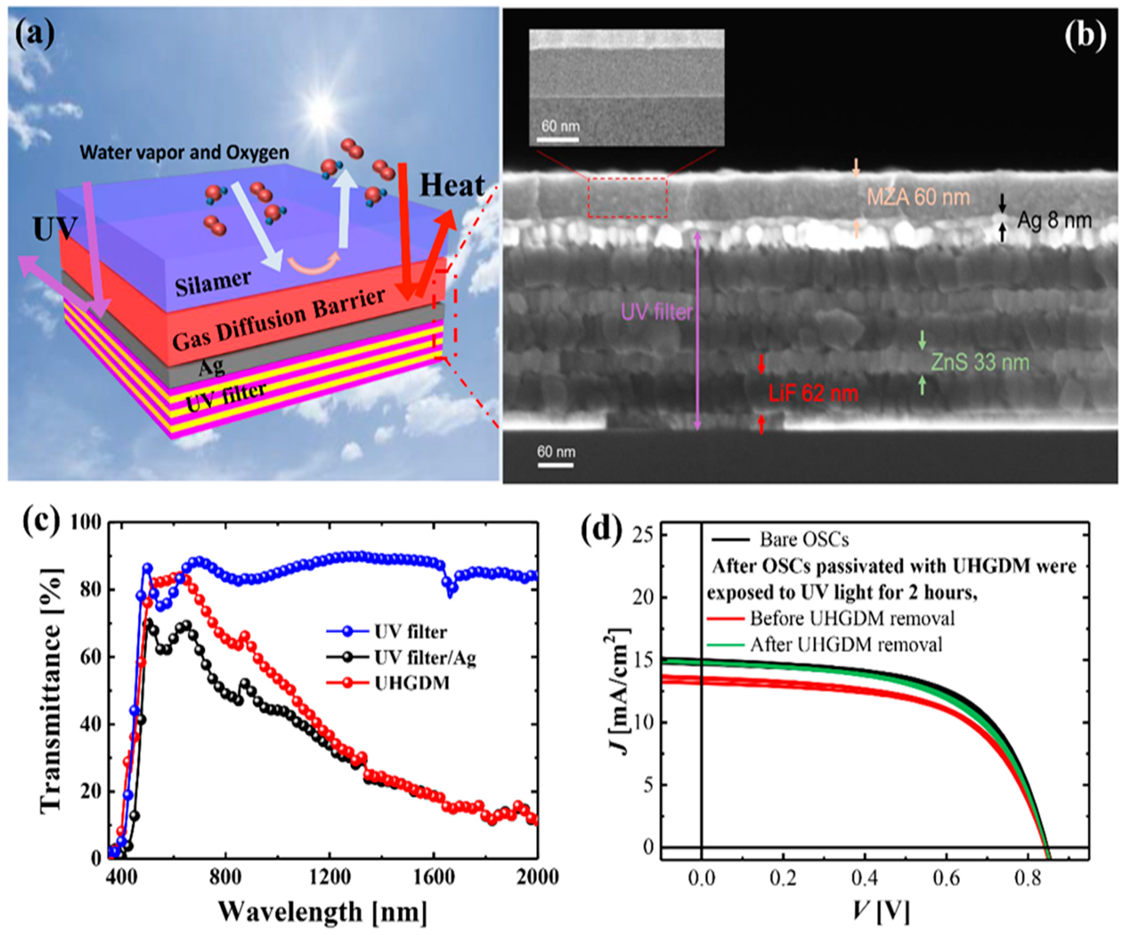
3.3. Functional Encapsulation with UV and Heat Rejection Capabilities
4. Corrosion-Resistant Wearable Encapsulations Using Chemical Bonding at the Interface between Thin Films
5. Future Works for the Development of Thin Film Encapsulation Technology
6. Conclusions
Author Contributions
Funding
Data Availability Statement
Conflicts of Interest
References
- Wong, W.S.; Salleo, A. (Eds.) Flexible Electronics: Materials and Applications; Springer Science & Business Media: Berlin, Germany, 2009; ISBN 9780387743622. [Google Scholar]
- Jørgensen, M.; Norrman, K.; Gevorgyan, S.A.; Tromholt, T.; Andreasen, B.; Krebs, F.C. Stability of Polymer Solar Cells. Adv. Mater. 2012, 24, 580–612. [Google Scholar] [CrossRef] [PubMed]
- Lange, J.; Wyser, Y. Recent Innovations in Barrier Technologies for Plastic Packaging—A Review. Packag. Technol. Sci. 2003, 16, 149–158. [Google Scholar] [CrossRef]
- Lewis, J. Material Challenge for Flexible Organic Devices. Mater. Today 2006, 9, 38–45. [Google Scholar] [CrossRef]
- Kim, W.; Kwon, S.; Han, Y.C.; Kim, E.; Choi, K.C.; Kang, S.H.; Park, B.C. Reliable Actual Fabric-Based Organic Light-Emitting Diodes: Toward a Wearable Display. Adv. Electron. Mater. 2016, 2, 1–7. [Google Scholar] [CrossRef]
- Lee, J.; Han, T.H.; Park, M.H.; Jung, D.Y.; Seo, J.; Seo, H.K.; Cho, H.; Kim, E.; Chung, J.; Choi, S.Y.; et al. Synergetic Electrode Architecture for Efficient Graphene-Based Flexible Organic Light-Emitting Diodes. Nat. Commun. 2016, 7, 11791. [Google Scholar] [CrossRef] [PubMed]
- Kwon, J.H.; Jeon, Y.; Kim, D.-G.; Lee, S.; Lee, S.; Kim, T.-S.; Choi, K.C. Low-Temperature and Corrosion-Resistant Gas Diffusion Multi-Barrier with UV and Heat Rejection Capability—A Strategy to Ensure Reliability of Organic Electronics. ACS Appl. Mater. Interfaces 2019, 11, 16776–16784. [Google Scholar] [CrossRef]
- Ono, S.; Häusermann, R.; Chiba, D.; Shimamura, K.; Ono, T.; Batlogg, B. High Performance Organic Field-Effect Transistors with Ultra-Thin HfO2 Gate Insulator Deposited Directly onto the Organic Semiconductor. Appl. Phys. Lett. 2014, 104, 013307. [Google Scholar] [CrossRef]
- Wang, C.Y.; Fuentes-Hernandez, C.; Yun, M.; Singh, A.; Dindar, A.; Choi, S.; Graham, S.; Kippelen, B. Organic Field-Effect Transistors with a Bilayer Gate Dielectric Comprising an Oxide Nanolaminate Grown by Atomic Layer Deposition. ACS Appl. Mater. Interfaces 2016, 8, 29872–29876. [Google Scholar] [CrossRef]
- Savagatrup, S.; Printz, A.D.; O’Connor, T.F.; Zaretski, A.V.; Rodriquez, D.; Sawyer, E.J.; Rajan, K.M.; Acosta, R.I.; Root, S.E.; Lipomi, D.J. Mechanical Degradation and Stability of Organic Solar Cells: Molecular and Microstructural Determinants. Energy Environ. Sci. 2015, 8, 55–80. [Google Scholar] [CrossRef]
- Moon, H.; Seong, H.; Shin, W.C.; Park, W.T.; Kim, M.; Lee, S.; Bong, J.H.; Noh, Y.Y.; Cho, B.J.; Yoo, S.; et al. Synthesis of Ultrathin Polymer Insulating Layers by Initiated Chemical Vapour Deposition for Low-Power Soft Electronics. Nat. Mater. 2015, 14, 628–635. [Google Scholar] [CrossRef]
- Jeong, E.G.; Jeon, Y.; Cho, S.H.; Choi, K.C. Textile-Based Washable Polymer Solar Cells for Optoelectronic Modules: Toward Self-Powered Smart Clothing. Energy Environ. Sci. 2019, 12, 1878–1889. [Google Scholar] [CrossRef]
- Logothetidis, S. Flexible Organic Electronic Devices: Materials, Process and Applications. Mater. Sci. Eng. B Solid-State Mater. Adv. Technol. 2008, 152, 96–104. [Google Scholar] [CrossRef]
- Choi, D.; Kim, S.-J.; Lee, J.H.; Chung, K.-B.; Park, J.-S. A Study of Thin Film Encapsulation on Polymer Substrate Using Low Temperature Hybrid ZnO/ Al2O3 Layers Atomic Layer Deposition. Curr. Appl. Phys. 2012, 12, S19–S23. [Google Scholar] [CrossRef]
- Nisato, G.; Kuilder, M.; Bouten, P.; Moro, L.; Philips, O.; Rutherford, N. Thin Film Encapsulation for OLEDs: Evaluation of Multi-Layer Barriers Using the Ca Test Measurement of Noise in the Optical System. In SID Symposium Digest of Technical Papers; Blackwell Publishing Ltd.: Oxford, UK, 2003; pp. 550–553. [Google Scholar]
- Lee, Y.I.; Jeon, N.J.; Kim, B.J.; Shim, H.; Yang, T.Y.; Seok, S.I.; Seo, J.; Im, S.G. A Low-Temperature Thin-Film Encapsulation for Enhanced Stability of a Highly Efficient Perovskite Solar Cell. Adv. Energy Mater. 2017, 8, 1701928. [Google Scholar] [CrossRef]
- Lee, S.; Han, J.H.; Lee, S.H.; Baek, G.H.; Park, J.S. Review of Organic/Inorganic Thin Film Encapsulation by Atomic Layer Deposition for a Flexible OLED Display. JOM 2019, 71, 197–211. [Google Scholar] [CrossRef]
- Kwon, J.H.; Choi, S.; Jeon, Y.; Kim, H.; Chang, K.S.; Choi, K.C. Functional Design of Dielectric-Metal-Dielectric-Based Thin-Film Encapsulation with Heat Transfer and Flexibility for Flexible Displays. ACS Appl. Mater. Interfaces 2017, 9, 27062–27072. [Google Scholar] [CrossRef]
- Han, Y.C.; Kim, E.; Kim, W.; Im, H.G.; Bae, B.S.; Choi, K.C. A Flexible Moisture Barrier Comprised of a SiO2-Embedded Organic-Inorganic Hybrid Nanocomposite and Al2O3 for Thin-Film Encapsulation of OLEDs. Org. Electron. 2013, 14, 1435–1440. [Google Scholar] [CrossRef]
- Kim, E.; Han, Y.; Kim, W.; Choi, K.C.; Im, H.G.; Bae, B.S. Thin Film Encapsulation for Organic Light Emitting Diodes Using a Multi-Barrier Composed of MgO Prepared by Atomic Layer Deposition and Hybrid Materials. Org. Electron. 2013, 14, 1737–1743. [Google Scholar] [CrossRef]
- Lee, S.M.; Kwon, J.H.; Kwon, S.; Choi, K.C. A Review of Flexible OLEDs toward Highly Durable Unusual Displays. IEEE Trans. Electron Devices 2017, 64, 1922–1931. [Google Scholar] [CrossRef]
- Lewis, J.S.; Weaver, M.S. Thin-Film Permeation-Barrier Technology for Flexible Organic Light-Emitting Devices. IEEE J. Sel. Top. Quantum Electron. 2004, 10, 45–57. [Google Scholar] [CrossRef]
- Kwon, J.H.; Kim, E.; Im, H.-G.; Bae, B.-S.; Chang, K.S.; Ko Park, S.-H.; Choi, K.C. Metal-Containing Thin-Film Encapsulation with Flexibility and Heat Transfer. J. Inf. Disp. 2015, 16, 123–128. [Google Scholar] [CrossRef]
- Han, Y.C.; Jeong, E.G.; Kim, H.; Kwon, S.; Im, H.-G.; Bae, B.-S.; Choi, K.C. Reliable Thin-Film Encapsulation of Flexible OLEDs and Enhancing Their Bending Characteristics through Mechanical Analysis. RSC Adv. 2016, 6, 40835–40843. [Google Scholar] [CrossRef]
- Kwon, J.H.; Jeon, Y.; Choi, K.C. Robust Transparent and Conductive Gas diffusion Multibarrier Based on Mg- and Al-Doped ZnO as Indium Tin Oxide-Free Electrodes for Organic Electronics. ACS Appl. Mater. Interfaces 2018, 10, 32387–32396. [Google Scholar] [CrossRef]
- Wang, L.; Ruan, C.; Li, M.; Zou, J.; Tao, H.; Peng, J.; Xu, M. Enhanced Moisture Barrier Performance for ALD-Encapsulated OLEDs by Introducing an Organic Protective Layer. J. Mater. Chem. C 2017, 5, 4017–4024. [Google Scholar] [CrossRef]
- Hoffmann, L.; Theirich, D.; Pack, S.; Kocak, F.; Schlamm, D.; Hasselmann, T.; Fahl, H.; Räupke, A.; Gargouri, H.; Riedl, T. Gas Diffusion Barriers Prepared by Spatial Atmospheric Pressure Plasma Enhanced ALD. ACS Appl. Mater. Interfaces 2017, 9, 4171–4176. [Google Scholar] [CrossRef]
- Kwon, J.H.; Jeon, Y.; Choi, S.; Kim, H.; Choi, K.C. Synergistic Gas Diffusion Multilayer Architecture Based on the Nanolaminate and Inorganic-Organic Hybrid Organic Layer. J. Inf. Disp. 2018, 19, 135–142. [Google Scholar] [CrossRef]
- Kwon, J.H.; Jeong, E.G.; Jeon, Y.; Kim, D.; Lee, S.; Choi, K.C. Design of Highly Water Resistant, Impermeable, and Flexible Thin- Film Encapsulation Based on Inorganic/Organic Hybrid Layers. ACS Appl. Mater. Interfaces 2019, 11, 3251–3261. [Google Scholar] [CrossRef]
- Behrendt, A.; Friedenberger, C.; Gahlmann, T.; Trost, S.; Becker, T.; Zilberberg, K.; Polywka, A.; Görrn, P.; Riedl, T. Highly Robust Transparent and Conductive Gas Diffusion Barriers Based on Tin Oxide. Adv. Mater. 2015, 27, 5961–5967. [Google Scholar] [CrossRef]
- Xiao, W.; Hui, D.Y.; Zheng, C.; Yu, D.; Qiang, Y.Y.; Ping, C.; Xiang, C.L.; Yi, Z. A Flexible Transparent Gas Barrier Film Employing the Method of Mixing ALD/MLD-Grown Al2O3 and Alucone Layers. Nanoscale Res. Lett. 2015, 10. [Google Scholar] [CrossRef]
- Jeong, S.Y.; Shim, H.R.; Na, Y.; Kang, K.S.; Jeon, Y.; Choi, S.; Jeong, E.G.; Park, Y.C.; Cho, H.E.; Lee, J.; et al. Foldable and Washable Textile-Based OLEDs with a Multi-Functional near-Room-Temperature Encapsulation Layer for Smart e-Textiles. npj Flex. Electron. 2021, 5, 15. [Google Scholar] [CrossRef]
- Kim, L.H.; Kim, K.; Park, S.; Jeong, Y.J.; Kim, H.; Chung, D.S.; Kim, S.H.; Park, C.E. Al2O3/TiO2 Nanolaminate Thin Film Encapsulation for Organic Thin Film Transistors via Plasma-Enhanced Atomic Layer Deposition. ACS Appl. Mater. Interfaces 2014, 6, 6731–6738. [Google Scholar] [CrossRef] [PubMed]
- Iatsunskyi, I.; Coy, E.; Viter, R.; Nowaczyk, G.; Jancelewicz, M.; Baleviciute, I.; Załęski, K.; Jurga, S. Study on Structural, Mechanical, and Optical Properties of Al2O3–TiO2 Nanolaminates Prepared by Atomic Layer Deposition. J. Phys. Chem. C 2015, 119, 20591–20599. [Google Scholar] [CrossRef]
- Meyer, J.; Schmidt, H.; Kowalsky, W.; Riedl, T.; Kahn, A. The Origin of Low Water Vapor Transmission Rates through Al2O3/ZrO2 Nanolaminate Gas-Diffusion Barriers Grown by Atomic Layer Deposition. Appl. Phys. Lett. 2010, 96, 243308. [Google Scholar] [CrossRef]
- Meyer, J.; Görrn, P.; Bertram, F.; Hamwi, S.; Winkler, T.; Johannes, H.-H.; Weimann, T.; Hinze, P.; Riedl, T.; Kowalsky, W. Al2O3/ZrO2 Nanolaminates as Ultrahigh Gas-Diffusion Barriers—A Strategy for Reliable Encapsulation of Organic Electronics. Adv. Mater. 2009, 21, 1845–1849. [Google Scholar] [CrossRef]
- Seo, S.-W.; Jung, E.; Chae, H.; Cho, S.M. Optimization of Al2O3/ZrO2 Nanolaminate Structure for Thin-Film Encapsulation of OLEDs. Org. Electron. 2012, 13, 2436–2441. [Google Scholar] [CrossRef]
- Choi, J.-H.; Kim, Y.-M.; Park, Y.-W.; Park, T.-H.; Jeong, J.-W.; Choi, H.-J.; Song, E.-H.; Lee, J.-W.; Kim, C.-H.; Ju, B.-K. Highly Conformal SiO2/Al2O3 Nanolaminate Gas-Diffusion Barriers for Large-Area Flexible Electronics Applications. Nanotechnology 2010, 21, 475203. [Google Scholar] [CrossRef]
- Chen, G.; Weng, Y.; Sun, F.; Zhou, X.; Wu, C.; Yan, Q.; Guo, T.; Zhang, Y. Low-Temperature Atomic Layer Deposition of Al2O3/Alucone Nanolaminates for OLED Encapsulation. RSC Adv. 2019, 9, 20884–20891. [Google Scholar] [CrossRef]
- Dameron, A.; Davidson, S.; Burton, B.; Carcia, P.; McLean, R.; George, S. Gas Diffusion Barriers on Polymers Using Multilayers Fabricated by Al2O3 and Rapid SiO2 Atomic Layer Deposition. J. Phys. Chem. C 2008, 112, 4573–4580. [Google Scholar] [CrossRef]
- Kwon, J.H.; Jeon, Y.; Choi, S.; Park, J.W.; Kim, H.; Choi, K.C. Functional Design of Highly Robust and Flexible Thin-Film Encapsulation Composed of Quasi-Perfect Sublayers for Transparent, Flexible Displays. ACS Appl. Mater. Interfaces 2017, 9, 43983–43992. [Google Scholar] [CrossRef]
- Gebhard, M.; Mai, L.; Banko, L.; Mitschker, F.; Hoppe, C.; Jaritz, M.; Kirchheim, D.; Zekorn, C.; de Los Arcos, T.; Grochla, D.; et al. PEALD of SiO2 and Al2O3 Thin Films on Polypropylene: Investigations of the Film Growth at the Interface, Stress and Gas Barrier Properties of Dyads. ACS Appl. Mater. Interfaces 2018, 10, 7422–7434. [Google Scholar] [CrossRef]
- Li, M.; Xu, M.; Zou, J.; Tao, H.; Wang, L.; Zhou, Z.; Peng, J. Realization of Al2O3 /MgO Laminated Structure at Low Temperature for Thin Film Encapsulation in Organic Light-Emitting Diodes. Nanotechnology 2016, 27, 494003. [Google Scholar] [CrossRef] [PubMed]
- Jeong, E.G.; Kwon, S.; Han, J.H.; Im, H.-G.; Bae, B.-S.; Choi, K.C. Mechanically Enhanced Hybrid Nano-Stratified Barrier with Defect Suppression Mechanism for Highly Reliable Flexible OLEDs. Nanoscale 2017, 6370–6379. [Google Scholar] [CrossRef]
- Yoon, K.H.; Kim, H.S.; Han, K.S.; Kim, S.H.; Lee, Y.E.K.; Shrestha, N.K.; Song, S.Y.; Sung, M.M. Extremely High Barrier Performance of Organic-Inorganic Nanolaminated Thin Films for Organic Light-Emitting Diodes. ACS Appl. Mater. Interfaces 2017, 9, 5399–5408. [Google Scholar] [CrossRef]
- Behrendt, A.; Meyer, J.; Van De Weijer, P.; Gahlmann, T.; Heiderhoff, R.; Riedl, T. Stress Management in Thin-Film Gas-Permeation Barriers. ACS Appl. Mater. Interfaces 2016, 8, 4056–4061. [Google Scholar] [CrossRef] [PubMed]
- Kang, K.S.; Jeong, S.Y.; Jeong, E.G.; Choi, K.C. Reliable High Temperature, High Humidity Flexible Thin Film Encapsulation Using Al2O3/MgO Nanolaminates for Flexible OLEDs. Nano Res. 2020, 13, 2716–2725. [Google Scholar] [CrossRef]
- Zhang, H.; Ding, H.; Wei, M.; Li, C.; Wei, B.; Zhang, J. Thin Film Encapsulation for Organic Light-Emitting Diodes Using Inorganic/Organic Hybrid Layers by Atomic Layer Deposition. Nanoscale Res. Lett. 2015, 10, 4–8. [Google Scholar] [CrossRef] [PubMed]
- Sun, F.-B.; Duan, Y.; Yang, Y.-Q.; Chen, P.; Duan, Y.-H.; Wang, X.; Yang, D.; Xue, K.-w. Fabrication of Tunable [Al2O3:Alucone] Thin-Film Encapsulations for Top-Emitting Organic Light-Emitting Diodes with High Performance Optical and Barrier Properties. Org. Electron. 2014, 15, 2546–2552. [Google Scholar] [CrossRef]
- Lee, B.H.; Yoon, B.; Abdulagatov, A.I.; Hall, R.A.; George, S.M. Growth and Properties of Hybrid Organic-Inorganic Metalcone Films Using Molecular Layer Deposition Techniques. Adv. Funct. Mater. 2013, 23, 532–546. [Google Scholar] [CrossRef]
- Park, J.; Ham, H.; Park, C. Heat Transfer Property of Thin-Film Encapsulation for OLEDs. Org. Electron. 2011, 12, 227–233. [Google Scholar] [CrossRef]
- Chung, S.; Lee, J.-H.; Jeong, J.; Kim, J.-J.; Hong, Y. Substrate Thermal Conductivity Effect on Heat Dissipation and Lifetime Improvement of Organic Light-Emitting Diodes. Appl. Phys. Lett. 2009, 94, 253302. [Google Scholar] [CrossRef]
- Kwon, J.H.; Im, H.; Bae, B.; Chang, K.S.; Park, S.K.; Choi, K.C. Heat Transferable Thin Film Encapsulation Inserted Ag Thin Film to Improve Reliability of Flexible Displays. In Proceedings of the SID Symposium Digest of Technical Papers, San Francisco, CA, USA, 22–27 May 2016; pp. 1491–1494. [Google Scholar]
- Ngo, I.L.; Jeon, S.; Byon, C. Thermal Conductivity of Transparent and Flexible Polymers Containing Fillers: A Literature Review. Int. J. Heat Mass Transf. 2016, 98, 219–226. [Google Scholar] [CrossRef]
- Azrain, M.M.; Mansor, M.R.; Fadzullah, S.H.S.M.; Omar, G.; Sivakumar, D.; Lim, L.M.; Nordin, M.N.A. Analysis of Mechanisms Responsible for the Formation of Dark Spots in Organic Light Emitting Diodes (OLEDs): A Review. Synth. Met. 2018, 235, 160–175. [Google Scholar] [CrossRef]
- Jeon, Y.; Choi, H.-R.; Lim, M.; Choi, S.; Kim, H.; Kwon, J.H.; Park, K.-C.; Choi, K.C. A Wearable Photobiomodulation Patch Using a Flexible Red-Wavelength OLED and Its In Vitro Differential Cell Proliferation Effects. Adv. Mater. Technol. 2018, 1700391, 1700391. [Google Scholar] [CrossRef]
- Bae, S.; Kim, H.K.; Lee, Y.; Xu, X.; Park, J.-S.; Zheng, Y.; Balakrishnan, J.; Im, D.; Lei, T.; Song, Y.I.; et al. 30 Inch Roll-Based Production of High-Quality Graphene Films for Flexible Transparent Electrodes. Nat. Nanotechnol. 2010, 5, 574–578. [Google Scholar] [CrossRef]
- Kim, S.H.; Song, W.; Jung, M.W.; Kang, M.A.; Kim, K.; Chang, S.J.; Lee, S.S.; Lim, J.; Hwang, J.; Myung, S.; et al. Carbon Nanotube and Graphene Hybrid Thin Film for Transparent Electrodes and Field Effect Transistors. Adv. Mater. 2014, 26, 4247–4252. [Google Scholar] [CrossRef]
- Seo, H.K.; Park, M.H.; Kim, Y.H.; Kwon, S.J.; Jeong, S.H.; Lee, T.W. Laminated Graphene Films for Flexible Transparent Thin Film Encapsulation. ACS Appl. Mater. Interfaces 2016, 8, 14725–14731. [Google Scholar] [CrossRef]
- Choi, K.; Nam, S.; Lee, Y.; Lee, M.; Jang, J.; Kim, S.J.; Jeong, Y.J.; Kim, H.; Bae, S.; Yoo, J.B.; et al. Reduced Water Vapor Transmission Rate of Graphene Gas Barrier Films for Flexible Organic Field-Effect Transistors. ACS Nano 2015, 9, 5818–5824. [Google Scholar] [CrossRef]
- Kwon, J.H.; Park, J.; Lee, M.K.; Park, J.W.; Jeon, Y.; Shin, J.B.; Nam, M.; Kim, C.-K.; Choi, Y.-K.; Choi, K.C. Low-Temperature Fabrication of Robust, Transparent, and Flexible Thin-Film Transistors with a Nanolaminated Insulator. ACS Appl. Mater. Interfaces 2018, 10, 15829–15840. [Google Scholar] [CrossRef]
- Guillén, C.; Herrero, J. Stability of Sputtered ITO Thin Films to the Damp-Heat Test. Surf. Coat. Technol. 2006, 201, 309–312. [Google Scholar] [CrossRef]
- Oh, S.J.; Kwon, J.H.; Lee, S.; Choi, K.C.; Kim, T.S. Unveiling the Annealing-Dependent Mechanical Properties of Freestanding Indium Tin Oxide Thin Films. ACS Appl. Mater. Interfaces 2021, 13, 16650–16659. [Google Scholar] [CrossRef]
- Yun, J. Ultrathin Metal Films for Transparent Electrodes of Flexible Optoelectronic Devices. Adv. Funct. Mater. 2017, 27, 1606641. [Google Scholar] [CrossRef]
- Chou, C.T.; Yu, P.W.; Tseng, M.H.; Hsu, C.C.; Shyue, J.J.; Wang, C.C.; Tsai, F.Y. Transparent Conductive Gas-Permeation Barriers on Plastics by Atomic Layer Deposition. Adv. Mater. 2013, 25, 1750–1754. [Google Scholar] [CrossRef] [PubMed]
- Hu, T.; Becker, T.; Pourdavoud, N.; Zhao, J.; Brinkmann, K.O.; Heiderhoff, R.; Gahlmann, T.; Huang, Z.; Olthof, S.; Meerholz, K.; et al. Indium-Free Perovskite Solar Cells Enabled by Impermeable Tin-Oxide Electron Extraction Layers. Adv. Mater. 2017, 29, 1606656. [Google Scholar] [CrossRef] [PubMed]
- Kwon, S.K.; Baek, J.H.; Choi, H.C.; Kim, S.K.; Lampande, R.; Pode, R.; Kwon, J.H. Degradation of OLED Performance by Exposure to UV Irradiation. RSC Adv. 2019, 9, 42561–42568. [Google Scholar] [CrossRef]
- Kim, E.; Jang, W.J.; Kim, W.; Park, J.; Lee, M.K.; Park, S.H.K.; Choi, K.C. Suppressed Instability of A-IGZO Thin-Film Transistors under Negative Bias Illumination Stress Using the Distributed Bragg Reflectors. IEEE Trans. Electron Devices 2016, 63, 1066–1071. [Google Scholar] [CrossRef]
- Kwon, S.; Kim, W.; Kim, H.; Choi, S.; Park, B.C.; Kang, S.H.; Choi, K.C. High Luminance Fiber-Based Polymer Light-Emitting Devices by a Dip-Coating Method. Adv. Electron. Mater. 2015, 1, 1500103. [Google Scholar] [CrossRef]
- Liang, J.; Li, L.; Niu, X.; Yu, Z.; Pei, Q. Elastomeric Polymer Light-Emitting Devices and Displays. Nat. Photonics 2013, 7, 817–824. [Google Scholar] [CrossRef]
- White, M.S.; Kaltenbrunner, M.; Głowacki, E.D.; Gutnichenko, K.; Kettlgruber, G.; Graz, I.; Aazou, S.; Ulbricht, C.; Egbe, D.A.M.; Miron, M.C.; et al. Ultrathin, Highly Flexible and Stretchable PLEDs. Nat. Photonics 2013, 7, 811–816. [Google Scholar] [CrossRef]
- Yokota, T.; Zalar, P.; Kaltenbrunner, M.; Jinno, H.; Matsuhisa, N.; Kitanosako, H.; Tachibana, Y.; Yukita, W.; Koizumi, M.; Someya, T. Ultraflexible Organic Photonic Skin. Sci. Adv. 2016, 2, e1501856. [Google Scholar] [CrossRef]
- Kim, K.; Hyun, B.G.; Jang, J.; Cho, E.; Park, Y.G.; Park, J.U. Nanomaterial-Based Stretchable and Transparent Electrodes. J. Inf. Disp. 2016, 17, 131–141. [Google Scholar] [CrossRef] [Green Version]
- Sekitani, T.; Nakajima, H.; Maeda, H.; Fukushima, T.; Aida, T.; Hata, K.; Someya, T. Stretchable Active-Matrix Organic Light-Emitting Diode Display Using Printable Elastic Conductors. Nat. Mater. 2009, 8, 494–499. [Google Scholar] [CrossRef] [PubMed]
- Liang, J.; Li, L.; Tong, K.; Ren, Z.; Hu, W.; Niu, X.; Chen, Y.; Pei, Q. Silver Nanowire Percolation Network Soldered with Graphene Oxide at Room Temperature and Its Application for Fully Stretchable Polymer Light-Emitting Diodes. ACS Nano 2014, 8, 1590–1600. [Google Scholar] [CrossRef] [PubMed]
- Lim, M.S.; Nam, M.; Choi, S.; Jeon, Y.; Son, Y.H.; Lee, S.M.; Choi, K.C. Two-Dimensionally Stretchable Organic Light-Emitting Diode with Elastic Pillar Arrays for Stress Relief. Nano Lett. 2020, 20, 1526–1535. [Google Scholar] [CrossRef] [PubMed]
- Yin, D.; Jiang, N.R.; Liu, Y.F.; Zhang, X.L.; Li, A.W.; Feng, J.; Sun, H.B. Mechanically Robust Stretchable Organic Optoelectronic Devices Built Using a Simple and Universal Stencil-Pattern Transferring Technology. Light Sci. Appl. 2018, 7, 35. [Google Scholar] [CrossRef]
- Kim, T.; Lee, H.; Jo, W.; Kim, T.S.; Yoo, S. Realizing Stretchable OLEDs: A Hybrid Platform Based on Rigid Island Arrays on a Stress-Relieving Bilayer Structure. Adv. Mater. Technol. 2020, 5, 2000494. [Google Scholar] [CrossRef]
- Choi, D.K.; Kim, D.H.; Lee, C.M.; Hafeez, H.; Sarker, S.; Yang, J.S.; Chae, H.J.; Jeong, G.W.; Choi, D.H.; Kim, T.W.; et al. Highly Efficient, Heat Dissipating, Stretchable Organic Light-Emitting Diodes Based on a MoO3/Au/MoO3 Electrode with Encapsulation. Nat. Commun. 2021, 12, 2864. [Google Scholar] [CrossRef]
- Kaltenbrunner, M.; Sekitani, T.; Reeder, J.; Yokota, T.; Kuribara, K.; Tokuhara, T.; Drack, M.; Schwödiauer, R.; Graz, I.; Bauer-Gogonea, S.; et al. An Ultra-Lightweight Design for Imperceptible Plastic Electronics. Nature 2013, 499, 458–463. [Google Scholar] [CrossRef]
- Call, J.; Varde, U.; Konson, A.; Walters, M.; Kotarba III, C.; Kraft, T.; Guha, S. Methodology and Systems to Ensure Reliable Thin-Film PV Modules. Reliab. Photovolt. Cells Modul. Compon. Syst. 2008, 7048, 70480S. [Google Scholar] [CrossRef]
- Turan, D. Water Vapor Transport Properties of Polyurethane Films for Packaging of Respiring Foods. Food Eng. Rev. 2021, 13, 54–65. [Google Scholar] [CrossRef]
- Koo, J.; Lee, S.; Kim, J.; Kim, D.H.; Choi, B.H.; Kim, T.S.; Shim, J.H. Evaluating Mechanical Properties of 100 nm-Thick Atomic Layer Deposited Al2O3 as a Free-Standing Film. Scr. Mater. 2020, 187, 256–261. [Google Scholar] [CrossRef]
- Rodriquez, D.; Kim, J.-H.; Root, S.E.; Fei, Z.; Boufflet, P.; Heeney, M.; Kim, T.-S.; Lipomi, D.J. Comparison of Methods for Determining the Mechanical Properties of Semiconducting Polymer Films for Stretchable Electronics. ACS Appl. Mater. Interfaces 2017, 9, 8855–8862. [Google Scholar] [CrossRef] [PubMed]


| ALD Nanolaminate | Achieved WVTR [g·m−2·day−1] (Test Condition) | Bending Test [g·m−2·day−1] (Bending Radius or Strain) | Environmental Stability Test (to Test or Not to Test) | Device Characteristics after Bending (Bending Radius or Strain) | Ref. |
|---|---|---|---|---|---|
| Al2O3/SiO2 | 4.2 × 10⁻⁵ (25 °C/40%) | X | X | X | [40] |
| Al2O3/ZrO2 | 4.7 × 10⁻⁵ (70 °C/70%) | X | X | X | [36] |
| Al2O3/SiO2 | 3.8 × 10⁻⁵ (20 °C/50%) | 1.64 × 10⁻³ (1 cm) | X | X | [38] |
| Al2O3/TiO2 | 1.81 × 10⁻⁴ (60 °C/90%) | X | O | X | [33] |
| Al2O3/alucone | 7.10 × 10⁻⁵ | 9.94 × 10⁻⁵ (0.105 mm) | X | X | [31] |
| Al2O3/MgO | 4.6 × 10⁻⁶ (60 °C/100%) | X | O | X | [43] |
| Al2O3/SAOLs | 1.58 × 10⁻³ (85 °C/85%) | 3.81 × 10⁻³ (1 cm) | X | X | [45] |
| Al2O3/ZnO | 7.87 × 10⁻⁶ (30 °C/90%) | 7.78 × 10⁻⁵ (1 cm) | X | 1 cm | [44] |
| Al2O3/ZnO/MgO | 2.44 × 10⁻⁶ (30 °C/90%) | 9.78 × 10⁻⁵ (0.6 cm) | O | 0.8 cm | [41] |
| Al2O3/MgO | 1.70 × 10⁻⁵ (30 °C/90%) | 9.78 × 10⁻⁵ (1.25%) | O | 0.63% | [47] |
| Al2O3/TiO2 | 9.94 × 10⁻⁶ (30 °C/90%) | ~10−5 (1.7%) | O | 0.15 cm | [32] |
Publisher’s Note: MDPI stays neutral with regard to jurisdictional claims in published maps and institutional affiliations. |
© 2022 by the authors. Licensee MDPI, Basel, Switzerland. This article is an open access article distributed under the terms and conditions of the Creative Commons Attribution (CC BY) license (https://creativecommons.org/licenses/by/4.0/).
Share and Cite
Jeon, Y.; Lee, H.; Kim, H.; Kwon, J.-H. A Review of Various Attempts on Multi-Functional Encapsulation Technologies for the Reliability of OLEDs. Micromachines 2022, 13, 1478. https://doi.org/10.3390/mi13091478
Jeon Y, Lee H, Kim H, Kwon J-H. A Review of Various Attempts on Multi-Functional Encapsulation Technologies for the Reliability of OLEDs. Micromachines. 2022; 13(9):1478. https://doi.org/10.3390/mi13091478
Chicago/Turabian StyleJeon, Yongmin, Hyeongjun Lee, Hyeunwoo Kim, and Jeong-Hyun Kwon. 2022. "A Review of Various Attempts on Multi-Functional Encapsulation Technologies for the Reliability of OLEDs" Micromachines 13, no. 9: 1478. https://doi.org/10.3390/mi13091478