Article

Low Leakage Current and High Breakdown Field AlGaN/GaN MIS-HEMTs Using PECVD-SiNx as a Gate Dielectric

1
Jiangsu Provincial Key Laboratory of Advanced Photonic and Electronic Materials, School of Electronic Science and Engineering, Nanjing University, Nanjing 210093, China
2
Microfabrication and Integration Technology Center, Nanjing University, Nanjing 210023, China
*
Author to whom correspondence should be addressed.
Micromachines 2022, 13(9), 1396; https://doi.org/10.3390/mi13091396
Submission received: 6 August 2022 / Revised: 21 August 2022 / Accepted: 24 August 2022 / Published: 26 August 2022

Abstract

:
In this paper, SiNx film deposited by plasma-enhanced chemical vapor deposition was employed as a gate dielectric of AlGaN/GaN high electron mobility transistors (HEMTs). We found that the NH3 flow during the deposition of SiNx can significantly affect the performances of metal–insulator–semiconductor (MIS) HEMTs. Compared to that without using NH3 flow, the device with the optimized NH3 flow exhibited three orders of magnitude lower gate leakage current, two orders of magnitude higher ON/OF drain current ratio, and an increased breakdown field by 69%. In addition, an in situ N2 plasma surface treatment prepared prior to SiNx deposition can further improve DC performances of MIS-HEMTs to a very low gate leakage current of 10−9 mA/mm and a high ON/OFF drain current ratio up to 109 by reducing the interface state density. These results demonstrate the great potential for using PECVD-SiNx as a gate dielectric in GaN-based MIS-HEMTs.

1. Introduction

Gallium nitride-based HEMTs have been considered excellent candidates for next-generation high-efficiency power switching devices due to their remarkable material and transport properties. However, conventional Schottky-gate HEMTs have a large gate leakage current and a small gate swing, which are limited by the Schottky-gate forward turn-on voltage (e.g., <3 V) [1,2]. To mitigate these issues, MIS-HEMTs have been proposed. It can suppress gate leakage and improve gate reliability by inserting an insulator between the gate metal and the barrier layer. Various dielectric materials are suitable as gate insulators, such as SiO2 [3], SiNx [4,5,6,7,8,9,10], Al2O3 [11,12], and SiON [13]. Among them, nitride-based gate dielectrics (e.g., SiNx) can avoid the additional introduction of interfacial Ga-O bonds, which tend to introduce interface traps and cause threshold voltage instability [4,14,15,16,17]. Currently, SiNx has been widely used as a gate dielectric/interfacial gate dielectric. There are many methods to deposit SiNx, such as plasma-enhanced chemical vapor deposition (PECVD) [1,18], low-pressure chemical vapor deposition (LPCVD) [4,5,6,8], and metal–organic chemical vapor deposition (MOCVD) [7,9].
Deposition methods, deposition conditions, and surface treatment before dielectric deposition can significantly affect the properties of SiNx films. Recently, LPCVD has been reported as a possible alternative technique for depositing high-quality SiNx [4,5,6,8]. However, dielectric deposition at a very high temperature is not compatible with typical microelectronic interconnect processing and may create surface defects due to the decomposition of GaN above 650 °C [19]. In situ SiNx grown by MOCVD may have Si contamination in the MOCVD chamber [5]. Compared with these gate dielectric deposition methods, using plasma-enhanced chemical vapor deposition (PECVD) SiNx shows great advantages in low temperature, easy operation, and high deposition rate [20,21,22]. PECVD-grown SiNx has been proven to be an effective material to suppress current collapse and reduce the surface states in AlGaN/GaN HEMTs.
In this work, we investigated the influence of SiNx deposition condition and surface treatment on the electrical properties of GaN-based MIS-HEMTs employing PECVD-SiNx as the gate dielectric. To evaluate the dielectric quality and interface properties, current–voltage (I–V) characterization, X-ray photoelectron spectroscopy (XPS), and capacitance–voltage (C–V) measurements were performed. The results showed that the optimized device exhibits a lower leakage current, a higher ON/OFF drain current, and a higher breakdown field than the device without any optimization.

2. Device Fabrication

To improve the breakdown field of the SiNx dielectric, we first optimized the deposition conditions of SiNx on Pt substrates using plasma-enhanced chemical vapor deposition by changing the flow of NH3. The reactant precursors were SiH4 (5%)/N2, NH3 and N2. The as-deposited 100 nm SiNx films were fabricated into metal–semiconductor–metal (MIM) capacitors for the measurements of breakdown field strength. The flow of NH3 was varied with a fixed SiH4: N2 ratio, a chamber pressure (=600 mtorr), and an RF power of 10 W. The results showed that NH3 flow could significantly affect the breakdown field of SiNx films, as presented in Figure 1a, and finally a maximum breakdown field of 11.45 MV/cm, which exceeds the reported breakdown field strength of PECVD-SiNx as a gate dielectric, was obtained at the condition of NH3 flow of 40 sccm.
The AlGaN/GaN heterostructure was grown by MOCVD on a silicon substrate. The epitaxial structure consisted of a 1-nm GaN cap layer, a 15-nm AlGaN barrier layer, a 1-nm AlN layer, a 4-µm GaN buffer layer, and an AlN nucleation layer, as shown schematically in Figure 1b. The use of AlN nucleation layer can release the tensile stress and reduce the dislocation defects on the epitaxial surface of GaN, thus improving the crystalline quality of GaN and reducing the cracking [23,24]. The device-fabrication started with electron beam evaporation of Ti/Al/Ni/Au and alloyed at 850 °C for 30 s in a N2 atmosphere to form an ohmic contact. The value of specific contact resistivity (ρc) of the ohmic contact was 3.39 × 10⁻⁵ Ω·cm2, as seen in Figure 1c,d [25,26]. Subsequently, a mesa isolation process was implemented by an inductively coupled plasma (ICP) system using a BCl3/Cl2 gas mixture. After that, 30-nm SiNx under the condition without NH3 gas was deposited for sample A and 30-nm SiNx under the condition with 40 sccm NH3 was deposited for sample B. Considering the effect of surface treatment, an in situ N2 plasma treatment before SiNx deposition, with NH3 gas flow of 40 sccm, was employed for sample C. The Ni/Au (50/100 nm) gate metal was then deposited by E-beam evaporation. Finally, the contact window was opened by a reactive ion etching (RIE) dry-etching system. The gate-to-source space is 4 µm, the gate-to-drain space is 12 µm, and the gate width and length are 100 µm and 4 µm, respectively. The fabricated devices were marked device A, B, and C, corresponding sample A, B, and C, respectively.

3. Results and Discussion

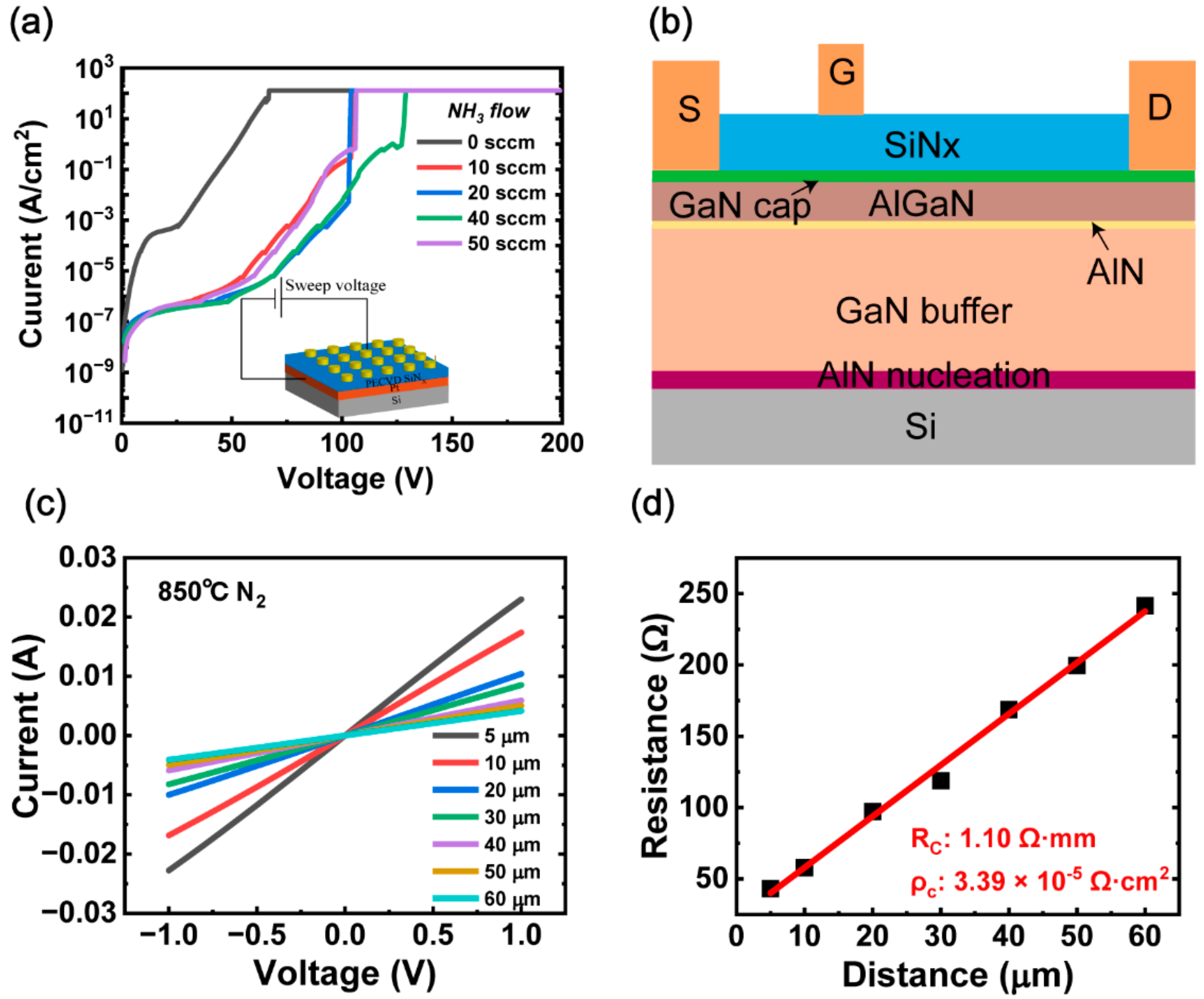
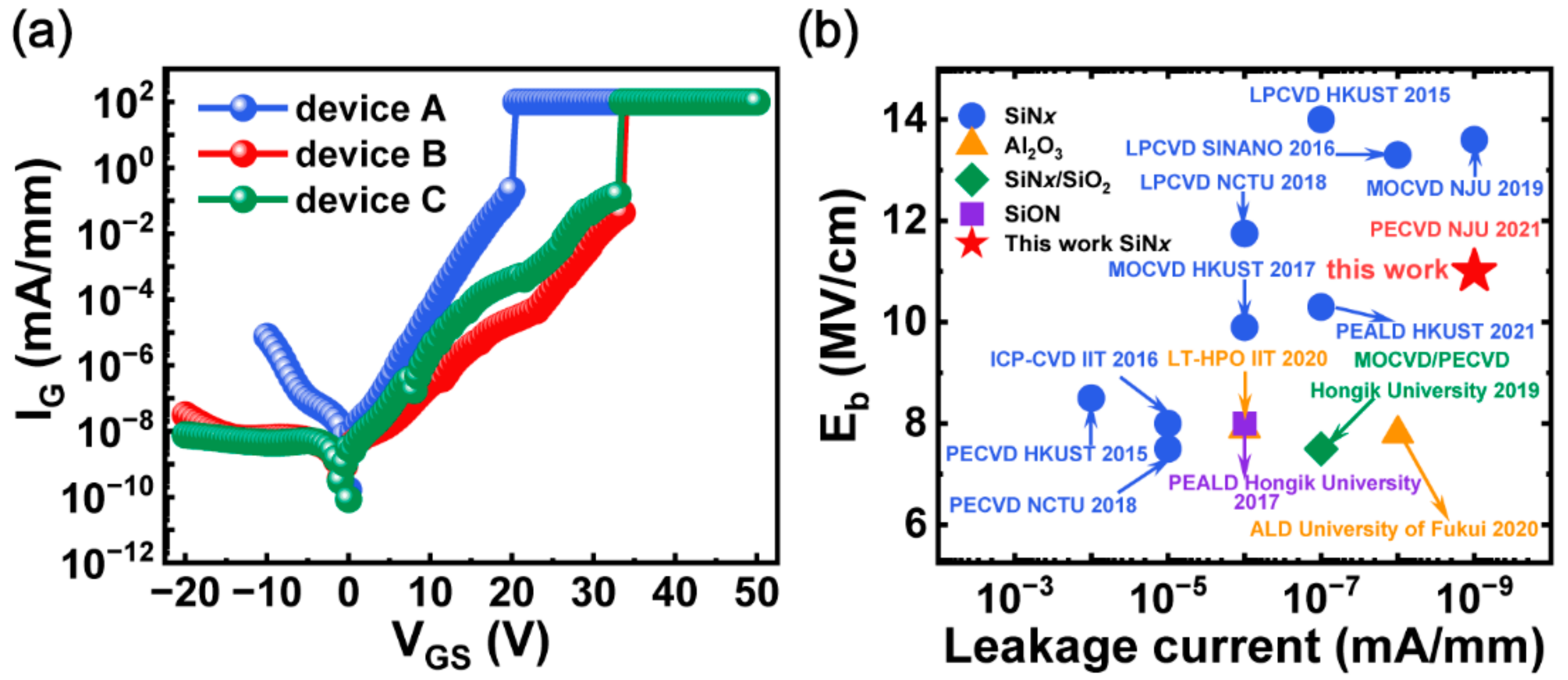
3.1. Material Optimization Characteristics

Figure 2 shows typical DC transfer, gate leakage, and output characteristics of PECVD-SiNx/AlGaN/GaN MIS-HEMTs. The transfer characteristics of MIS-HEMTs were measured at a drain bias voltage of 10 V. Compared with device A, device B exhibits a much higher ON/OFF drain current ratio of ~108. In addition, device B shows a very low gate leakage current of ~10−8 mA/mm at both VG = −20 V and VG = 10 V, three orders of magnitude lower than that of device A, suggesting that SiNx deposition with NH3 flow can effectively suppress leakage paths in the gate dielectric. In Figure 2b, device B shows a relatively larger threshold voltage hysteresis, compared with device A. This indicates that SiNx without NH3 can alleviate the surface trapping effect. Meanwhile, a large negative threshold voltage shift in device B may come from the high density of positive charges existing at the interface between SiNx and AlGaN [27]. In addition, these positive charges may be introduced by the hydrogen radicals originating from NH3. As shown in Figure 2c,d, device B shows a larger saturated output current of 608 mA/mm and a lower on-resistance of 8.9 Ω·mm, compared with device A.
To further understand the reasons for the improved electrical performances obtained by optimizing the NH3 flow, we analyzed the dielectric surface roughness and the N/Si ratio of SiNx with different deposition conditions by employing atomic force microscopy (AFM) and X-ray photoelectron spectroscopy (XPS). As shown in Figure 3a,b, the root mean square (RMS) roughness over a 5 µm × 5 µm area is 1.59 nm for SiNx without NH3, but 0.69 nm for SiNx with 40 sccm NH3, indicating that NH3 can effectively reduce the surface roughness of the SiNx dielectric. Typical Si 2p core-level spectrums were captured as shown in Figure 3c,d. Three components corresponding to Si-Si bonds, Si-N bonds, and Si-O bonds were extracted from the spectrum. The amount of elemental composition incorporation in SiNx was estimated in Table 1 by using the standard method, as reported in Ref. [28]. The SiNx stoichiometry (x = [N]/[Si]) was analyzed by the peak area sensitivity method [29], and the results showed that the corresponding N/Si ratio was changed from 0.75 to 1.05 before and after optimizing NH3 flow, respectively. Moreover, with the increase in N/Si ratio, the Si-Si bond contents decreased while the Si-O bond and Si-N bond contents increased. An increase in the N/Si ratio was demonstrated to be able to improve the insulation characteristics of the SiNx dielectric film, as reported in Refs. [27,30], which can explain why device B exhibits better DC characteristics than device A.

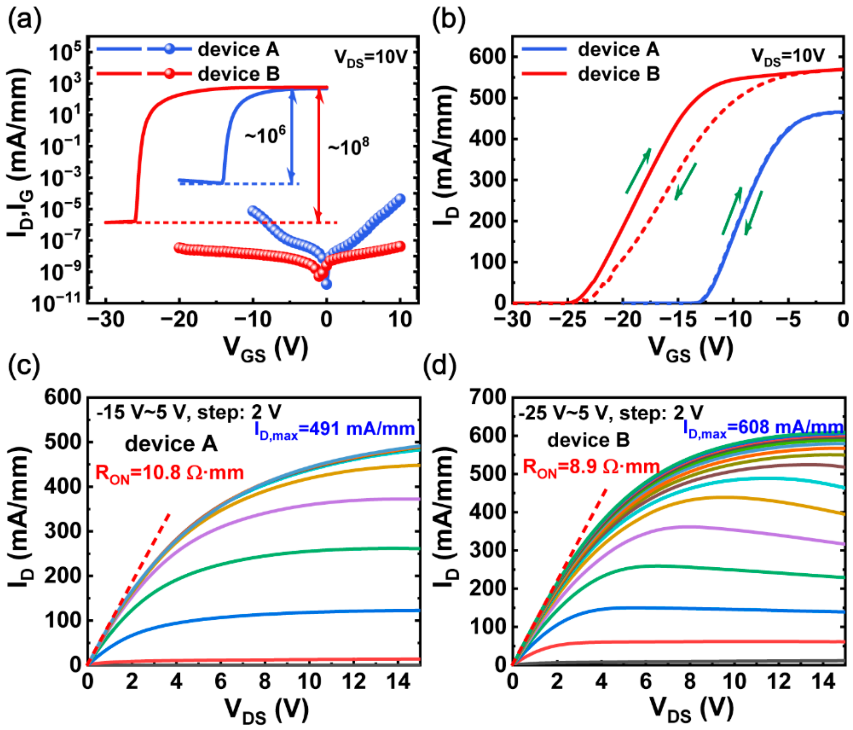
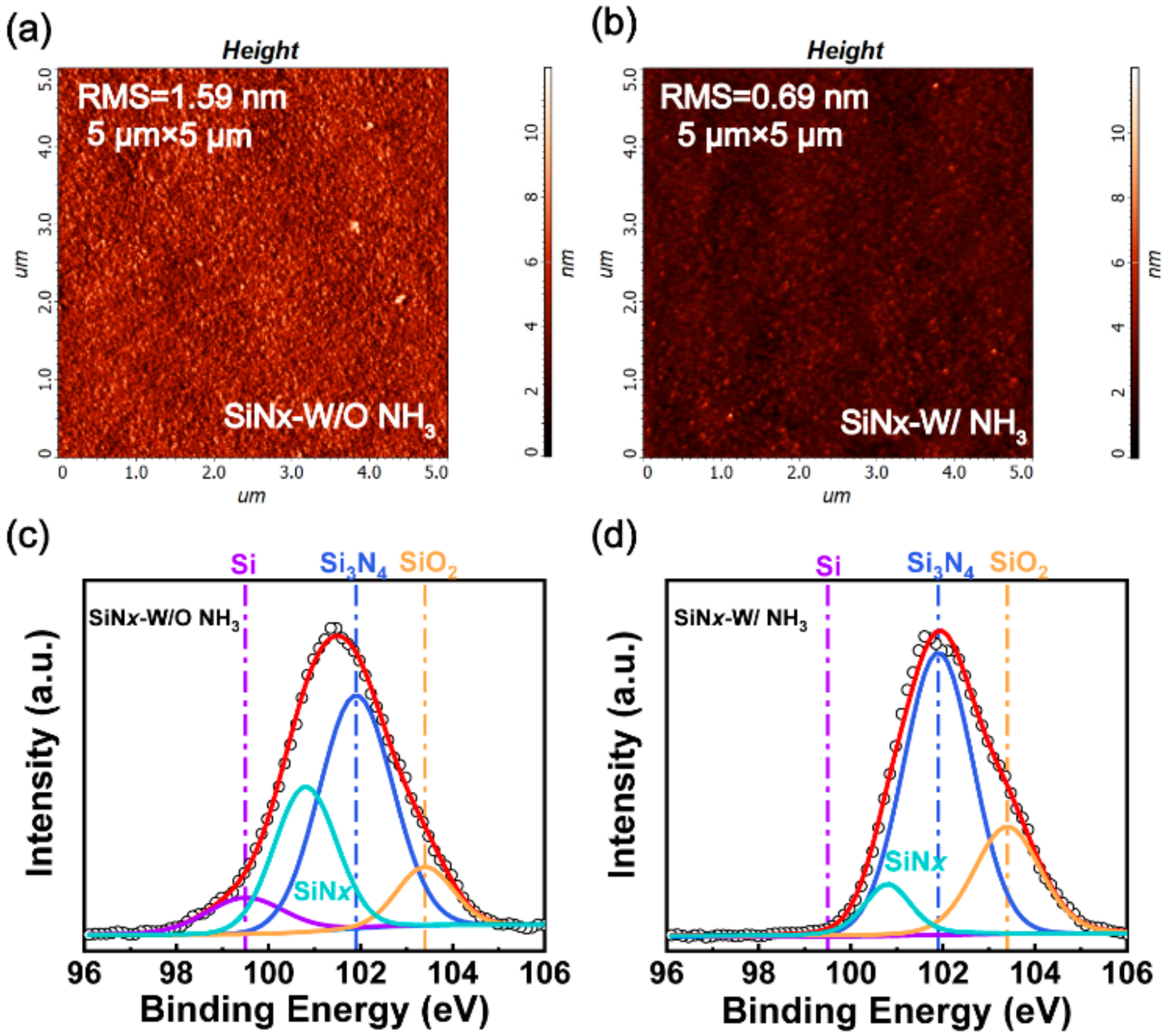
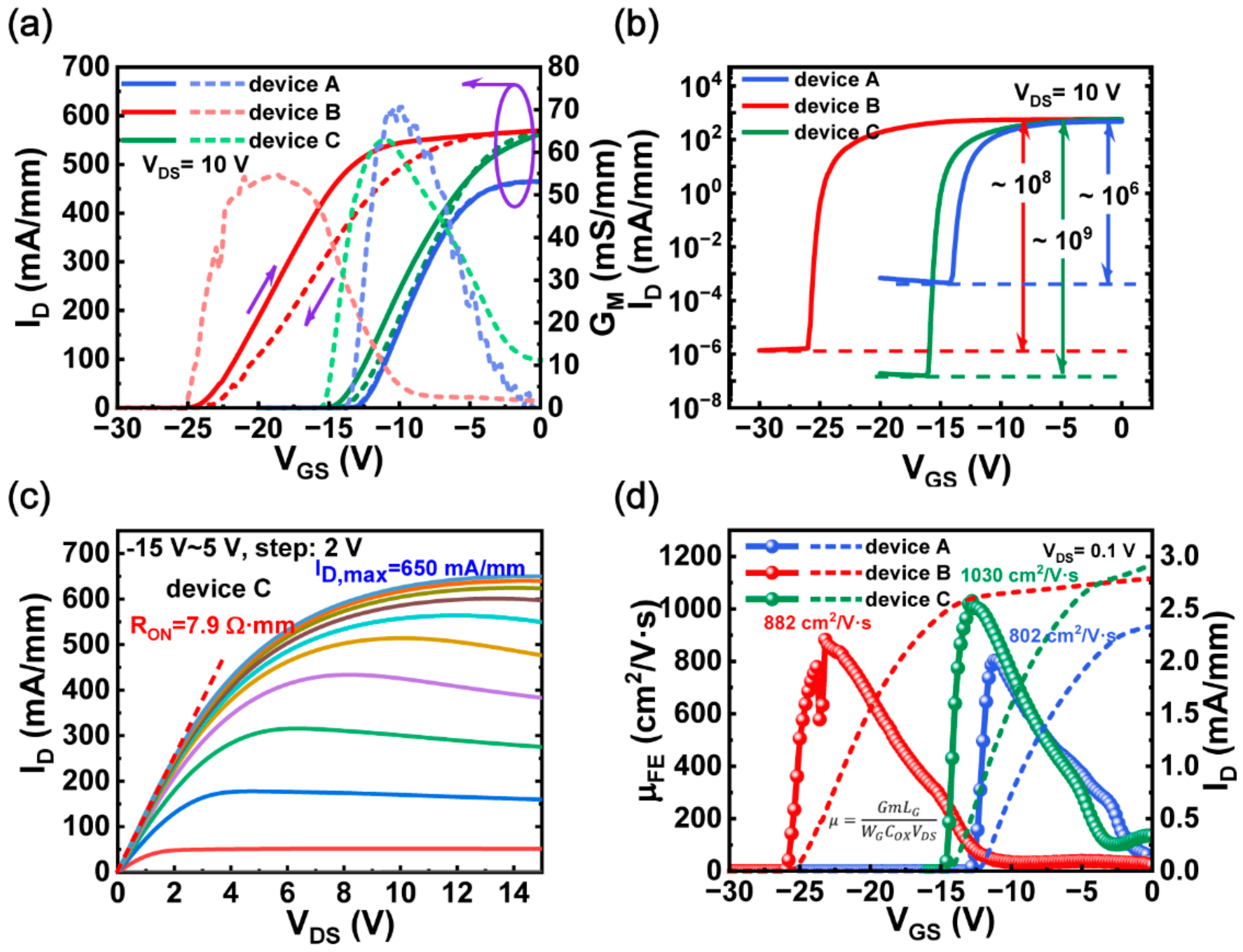
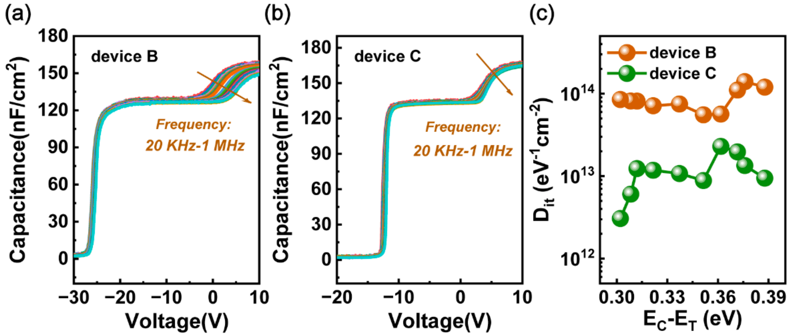
3.2. Interface Optimization Characteristics

However, device B shows a larger voltage hysteresis than device A, which may result from hydrogen radicals originating from NH3. It has been confirmed that NH3 can diffuse into the GaN structure and react with Ga-N bonds, thus resulting in the generation of nitrogen vacancies and Ga-H bonds near the surface [31,32]. To reduce these interface defects, some surface treatment methods have been well developed [33,34,35,36,37]. In this work, an in situ N2 plasma surface treatment was adopted before dielectric deposition for device C which has the same subsequent processes as device B. As shown in Figure 4a,b, device A shows the smallest VTH hysteresis and the lowest ON/OFF drain current ratio. In addition, it can be seen that the saturation current in device A is the smallest, indicating that device A has the lowest 2DEG concentration at the AlGaN/GaN interface. Device C exhibits a large positive shift of VTH compared to device B, which may be related to the reduction of nitrogen-vacancy defects, thus reducing the positive charges [34]. Meanwhile, the transconductance and ON/OFF drain current ratio (~109) of device C are further improved, indicating that in situ N2 plasma treatment can suppress the trapping of channel carriers by surface defects. Moreover, device C exhibits the lowest ON-resistance of 7.9 Ω·mm and the highest saturation output current up to 650 mA/mm in comparison with device A and B, which can be attributed to the improvement of field-effect mobility. As presented in Figure 4d, device C shows the highest field-effect mobility because of the improvement in device transconductance, thus reducing the on-resistance in device C. Since the on-resistance is mainly related to field-effect mobility and carrier concentration, device A has the largest on-resistance. Generally, after optimization, the maximum drain current and the field-effect mobility of device C increased by 32% and 28%, respectively, compared with device A.
Furthermore, the gate leakage characteristics of the MIS-HEMTs were measured at VDS = 0 V as shown in Figure 5. In comparison with device A, device B and C exhibit much lower gate leakage current and higher forward gate breakdown voltage up to 34 V at room temperature due to the optimized deposition condition of the SiNx dielectric with NH3 flow. The corresponding electric field strength (Eb) was estimated to be 11 MV/cm, a very competitive result referring to those of reported MIS-HEMTs. We benchmarked the gate leakage current versus electrical field against these reported AlGaN/GaN MIS-HEMTs [3,4,5,6,7,8,9,10,11,12,13,38], as plotted in Figure 5b. In general, the gate leakage and breakdown field of the optimized device in this work are comparable to those of the reported state-of-the-art AlGaN/GaN MIS-HEMTs.
Finally, capacitance–voltage (C–V) measurements were performed on the MIS diodes, corresponding to device B and C, with different frequencies varying from 20 kHz to 1 MHz at room temperature. As shown in Figure 6, there are two obvious steps in both C-V curves. The first step corresponds to the process of accumulating two-dimensional electron gas in the AlGaN/GaN heterojunction while the second step reflects the electron transfer from the AlGaN/GaN to the SiNx/GaN interfaces [39]. In comparison with device B, device C exhibits a smaller frequency dispersion in the second step, indicating a higher quality interface of SiNx/GaN that has a lower trap density. We also calculated the interface state density using the method in Ref. [40], and the results are shown in Figure 6c. We found that the interface state density was reduced by almost one order of magnitude after the in situ N2 plasma surface treatment indicating that nitrogen vacancies and surface oxygen-related bonds can be effectively reduced by an in situ N2 plasma treatment, thus obtaining a high-quality SiNx/GaN interface.

4. Conclusions

In summary, we studied the impact of SiNx growth condition and surface treatment on the electrical properties of AlGaN/GaN MIS-HEMTs when employing PECVD-SiNx as a gate dielectric. The results show that the gate leakage current can be greatly suppressed by increasing the N/Si ratio of SiNx, and the interface state density can be obviously reduced through in situ N2 plasma surface treatment. The optimized SiNx/AlGaN/GaN MIS-HEMTs exhibit low gate leakage current, high ION/IOFF ratio, and high breakdown field. These results prove that PECVD-SiNx/AlGaN/GaN MIS-HEMT is comparable to those of the reported state-of-the-art AlGaN/GaN MIS-HEMTs.

Author Contributions

Methodology, X.G.; investigation, X.G.; validation, H.G. and R.W.; writing—original draft preparation, X.G.; writing—review and editing, D.C.; supervision, D.P., P.C., H.L., R.Z. and Y.Z.; funding acquisition, D.C., D.P. and H.G. All authors have read and agreed to the published version of the manuscript.

Funding

This work was supported by the State Key R&D Project of Jiangsu Province, China (BE2022070-4, BE2021026), the National Natural Science Foundation of China (62104096) and China Postdoctoral Science Foundation (2022TQ0142).

Conflicts of Interest

The authors declare no conflict of interest.

References

  1. Tang, Z.; Jiang, Q.; Lu, Y.; Huang, S.; Yang, S.; Tang, X.; Chen, K.J. 600-V normally off SiNx/AlGaN/GaN MIS-HEMT with large gate swing and low current collapse. IEEE Electron Device Lett. 2013, 34, 1373–1375. [Google Scholar] [CrossRef]
  2. Hernández-Gutiérrez, C.A.; Kudriavtsev, Y.; Cardona, D.; Hernández, A.G.; Camas-Anzueto, J.L. Optical, electrical, and chemical characterization of nanostructured InxGa1-xN formed by high fluence In+ ion implantation into GaN. Opt. Mater. 2021, 111, 110541. [Google Scholar] [CrossRef]
  3. Cho, G.; Cha, H.Y.; Kim, H. Influence of Oxygen-Plasma Treatment on In-Situ SiN/AlGaN/GaN MOSHEMT with PECVD SiO2 Gate Insulator. Materials 2019, 12, 3968. [Google Scholar] [CrossRef] [PubMed]
  4. Hua, M.; Liu, C.; Yang, S.; Liu, S.; Fu, K.; Dong, Z.; Cai, Y.; Zhang, B.; Chen, K.J. Characterization of Leakage and Reliability of SiNx Gate Dielectric by Low-Pressure Chemical Vapor Deposition for GaN-based MIS-HEMTs. IEEE Trans. Electron Devices 2015, 62, 3215–3222. [Google Scholar] [CrossRef]
  5. Hua, M.; Liu, C.; Yang, S.; Liu, S.; Fu, K.; Dong, Z.; Cai, Y.; Zhang, B.; Chen, K.J. GaN-Based Metal-Insulator-Semiconductor High-Electron-Mobility Transistors Using Low-Pressure Chemical Vapor Deposition SiNx as Gate Dielectric. IEEE Electron Device Lett. 2015, 36, 448–450. [Google Scholar] [CrossRef]
  6. Zhang, Z.; Yu, G.; Zhang, X.; Deng, X.; Li, S.; Fan, Y.; Sun, S.; Song, L.; Tan, S.; Wu, D.; et al. Studies on High-Voltage GaN-on-Si MIS-HEMTs Using LPCVD Si3N4as Gate Dielectric and Passivation Layer. IEEE Trans. Electron Devices 2016, 63, 731–738. [Google Scholar] [CrossRef]
  7. Jiang, H.; Liu, C.; Chen, Y.; Lu, X.; Tang, C.W.; Lau, K.M. Investigation of In Situ SiN as Gate Dielectric and Surface Passivation for GaN MISHEMTs. IEEE Trans. Electron Devices 2017, 64, 832–839. [Google Scholar] [CrossRef]
  8. Wang, H.-C.; Lumbantoruan, F.J.; Hsieh, T.-E.; Wu, C.-H.; Lin, Y.-C.; Chang, E.Y. High-Performance LPCVD-SiNx/InAlGaN/GaN MIS-HEMTs with 850-V 0.98-mΩ·cm2 for Power Device Applications. IEEE J. Electron Devices Soc. 2018, 6, 1136–1141. [Google Scholar] [CrossRef]
  9. Cheng, L.; Xu, W.; Pan, D.; Liang, H.; Wang, R.; Zhu, Y.; Ren, F.; Zhou, D.; Ye, J.; Chen, D.; et al. Gate-first AlGaN/GaN HEMT technology for enhanced threshold voltage stability based on MOCVD-grown in situ SiNx. J. Phys. D Appl. Phys. 2021, 54, 015105. [Google Scholar] [CrossRef]
  10. Dutta, G.; DasGupta, N.; DasGupta, A. Low-Temperature ICP-CVD SiNx as Gate Dielectric for GaN-Based MIS-HEMTs. IEEE Trans. Electron Devices 2016, 63, 4693–4701. [Google Scholar] [CrossRef]
  11. Asubar, J.T.; Kawabata, S.; Tokuda, H.; Yamamoto, A.; Kuzuhara, M. Enhancement-Mode AlGaN/GaN MIS-HEMTs with High VTH and High IDmax Using Recessed-Structure with Regrown AlGaN Barrier. IEEE Electron Device Lett. 2020, 41, 693–696. [Google Scholar] [CrossRef]
  12. Kanaga, S.; Dutta, G.; Kushwah, B.; DasGupta, N.; DasGupta, A. Low Temperature and High Pressure Oxidized Al2O3 as Gate Dielectric for AlInN/GaN MIS-HEMTs. IEEE Trans. Device Mater. Reliab. 2020, 20, 613–621. [Google Scholar] [CrossRef]
  13. Kim, H.-S.; Han, S.-W.; Jang, W.-H.; Cho, C.-H.; Seo, K.-S.; Oh, J.; Cha, H.-Y. Normally-off GaN-on-Si MISFET Using PECVD SiON Gate Dielectric. IEEE Electron Device Lett. 2017, 38, 1090–1093. [Google Scholar] [CrossRef]
  14. Huang, S.; Yang, S.; Roberts, J.; Chen, K.J. Threshold Voltage Instability in Al2O3/GaN/AlGaN/GaN Metal–Insulator–Semiconductor High-Electron Mobility Transistors. Jpn. J. Appl. Phys. 2011, 50, 110202. [Google Scholar] [CrossRef]
  15. Lu, Y.; Yang, S.; Jiang, Q.; Tang, Z.; Li, B.; Chen, K.J. Characterization of VT-instability in enhancement-mode Al2O3-AlGaN/GaN MIS-HEMTs. Phys. Status Solidi C 2013, 10, 1397–1400. [Google Scholar] [CrossRef]
  16. Ma, X.-H.; Zhu, J.-J.; Liao, X.-Y.; Yue, T.; Chen, W.-W.; Hao, Y. Quantitative characterization of interface traps in Al2O3/AlGaN/GaN metal-oxide-semiconductor high-electron-mobility transistors by dynamic capacitance dispersion technique. Appl. Phys. Lett. 2013, 103, 033510. [Google Scholar] [CrossRef]
  17. Yang, S.; Tang, Z.; Wong, K.-Y.; Lin, Y.-S.; Liu, C.; Lu, Y.; Huang, S.; Chen, K.J. High-Quality Interface in Al2O3/GaN/AlGaN/GaN MIS Structures with In Situ Pre-Gate Plasma Nitridation. IEEE Electron Device Lett. 2013, 34, 1497–1499. [Google Scholar] [CrossRef]
  18. Hove, M.V.; Boulay, S.; Bahl, S.R.; Stoffels, S.; Kang, X.; Wellekens, D.; Geens, K.; Delabie, A.; Decoutere, S. CMOS Process-Compatible High-Power Low-Leakage AlGaN/GaN MISHEMT on Silicon. IEEE Electron Device Lett. 2012, 33, 667–669. [Google Scholar] [CrossRef]
  19. Maier, D.; Alomari, M.; Grandjean, N.; Carlin, J.-F.; Diforte-Poisson, M.-A.; Dua, C.; Chuvilin, A.; Troadec, D.; Gaquiere, C.; Kaiser, U.; et al. Testing the Temperature Limits of GaN-Based HEMT Devices. IEEE Trans. Device Mater. Reliab. 2010, 10, 427–436. [Google Scholar] [CrossRef]
  20. Yota, J.; Hander, J.; Saleh, A.A. A comparative study on inductively-coupled plasma high-density plasma, plasma-enhanced, and lowpressure chemical vapor deposition silicon nitride films. J. Vac. Sci. Technol. A 2000, 18, 372–376. [Google Scholar] [CrossRef]
  21. Guler, I. Optical and structural characterization of silicon nitride thin films deposited by PECVD. Mater. Sci. Eng. B 2019, 246, 21–26. [Google Scholar] [CrossRef]
  22. Piccirillo, A.; Gobbi, A.L. Physical-Electrical Properties of Silicon Nitride Deposited by PECVD on III–V Semiconductors. J. Electrochem. Soc. 1990, 137, 3910–3917. [Google Scholar] [CrossRef]
  23. Zambrano-Serrano, M.A.; Hernández, C.A.; de Melo, O.; Behar, M.; Gallardo-Hernández, S.; Casallas-Moreno, Y.L.; Ponce, A.; Hernandez-Robles, A.; Bahena-Uribe, D.; Yee-Rendón, C.M.; et al. Effects of heavy Si doping on the structural and optical properties of n-GaN/AlN/Si(111) heterostructures. Mater. Res. Express 2022, 9, 065903. [Google Scholar] [CrossRef]
  24. Pan, L.; Dong, X.; Li, Z.; Luo, W.; Ni, J. Influence of the AlN nucleation layer on the properties of AlGaN/GaN heterostructure on Si (1 1 1) substrates. Appl. Surf. Sci. 2018, 447, 512–517. [Google Scholar] [CrossRef]
  25. Greco, G.; Prystawko, P.; Leszczyński, M.; Lo Nigro, R.; Raineri, V.; Roccaforte, F. Electro-structural evolution and Schottky barrier height in annealed Au/Ni contacts onto p-GaN. J. Appl. Phys. 2011, 110, 123703. [Google Scholar] [CrossRef]
  26. Hernández-Gutierrez, C.A.; Kudriavtsev, Y.; Mota, E.; Hernández, A.G.; Escobosa-Echavarría, A.; Sánchez-Resendiz, V.; Casallas-Moreno, Y.L.; López-López, M. A new method of making ohmic contacts to p-GaN. Nucl. Instrum. Methods Phys. Res. B 2016, 388, 35–40. [Google Scholar] [CrossRef]
  27. Huang, T.; Jiang, H.; Bergsten, J.; Lau, K.M.; Rorsman, N. Enhanced gate stack stability in GaN transistors with gate dielectric of bilayer SiNx by low pressure chemical vapor deposition. Appl. Phys. Lett. 2018, 113, 232102. [Google Scholar] [CrossRef]
  28. Nayak, S.K.; Gupta, M.; Shivaprasad, S.M. Structural, optical and electronic properties of a Mg incorporated GaN nanowall network. RSC Adv. 2017, 7, 25998–26005. [Google Scholar] [CrossRef]
  29. Siddique, A.; Ahmed, R.; Anderson, J.; Holtz, M.; Piner, E.L. Improved Electrical Properties of AlGaN/GaN High-Electron-Mobility Transistors by In Situ Tailoring the SiNx Passivation Layer. ACS Appl. Mater. Interfaces 2021, 13, 18264–18273. [Google Scholar] [CrossRef]
  30. Gupta, M.; Rathi, V.K.; Thangaraj, R.; Agnihotri, O.P. The preparation, properties and applications of silicon nitride thin films deposited by plasma-enhanced chemical vapor deposition. Thin Solid Films 1991, 204, 77–106. [Google Scholar] [CrossRef]
  31. Hashizume, T.; Nakasaki, R. Discrete surface state related to nitrogen-vacancy defect on plasma-treated GaN surfaces. Appl. Phys. Lett. 2002, 80, 4564–4566. [Google Scholar] [CrossRef]
  32. Puzyrev, Y.S.; Roy, T.; Beck, M.; Tuttle, B.R.; Schrimpf, R.D.; Fleetwood, D.M.; Pantelides, S.T. Dehydrogenation of defects and hot-electron degradation in GaN high-electron-mobility transistors. J. Appl. Phys. 2011, 109, 034501. [Google Scholar] [CrossRef]
  33. Liu, S.-C.; Chen, B.-Y.; Lin, Y.-C.; Hsieh, T.-E.; Wang, H.-C.; Chang, E.Y. GaN MIS-HEMTs with Nitrogen Passivation for Power Device Applications. IEEE Electron Device Lett. 2014, 35, 1001–1003. [Google Scholar]
  34. Liu, S.-C.; Trinh, H.-D.; Dai, G.-M.; Huang, C.-K.; Dee, C.-F.; Majlis, B.Y.; Biswas, D.; Chang, E.Y. Effective surface treatment for GaN metal–insulator–semiconductor high-electron-mobility transistors using HF plus N2 plasma prior to SiN passivation. Jpn. J. Appl. Phys. 2016, 55, 01AD06. [Google Scholar] [CrossRef]
  35. Zhu, J.; Ma, X.; Hou, B.; Ma, M.; Zhu, Q.; Chen, L.; Yang, L.; Zhang, P.; Zhou, X.; Hao, Y. Comparative Study on Charge Trapping Induced Vth Shift for GaN-Based MOS-HEMTs with and without Thermal Annealing Treatment. IEEE Trans. Electron Devices 2018, 65, 5343–5349. [Google Scholar] [CrossRef]
  36. Lu, X.; Jiang, H.; Liu, C.; Zou, X.; Lau, K.M. Off-state leakage current reduction in AlGaN/GaN high electron mobility transistors by combining surface treatment and post-gate annealing. Semicond. Sci. Technol. 2016, 31, 055019. [Google Scholar] [CrossRef]
  37. Lin, S.; Wang, M.; Xie, B.; Wen, C.P.; Yu, M.; Wang, J.; Hao, Y.; Wu, W.; Huang, S.; Chen, K.J.; et al. Reduction of Current Collapse in GaN High-Electron Mobility Transistors Using a Repeated Ozone Oxidation and Wet Surface Treatment. IEEE Electron Device Lett. 2015, 36, 757–759. [Google Scholar]
  38. Yang, S.; Zheng, Z.; Zhang, L.; Song, W.; Chen, K.J. GaN MIS-HEMTs with Surface Reinforcement for Suppressed Hot-Electron-Induced Degradation. IEEE Electron Device Lett. 2021, 42, 489–492. [Google Scholar] [CrossRef]
  39. Mizue, C.; Hori, Y.; Miczek, M.; Hashizume, T. Capacitance–Voltage Characteristics of Al2O3/AlGaN/GaN Structures and State Density Distribution at Al2O3/AlGaN Interface. Jpn. J. Appl. Phys. 2011, 50, 021001. [Google Scholar] [CrossRef]
  40. Yang, S.; Liu, S.; Lu, Y.; Liu, C.; Chen, K.J. AC-Capacitance Techniques for Interface Trap Analysis in GaN-Based Buried-Channel MIS-HEMTs. IEEE Trans. Electron Devices 2015, 62, 1870–1878. [Google Scholar] [CrossRef]
Figure 1. (a) Forward leakage current characteristics for circular MIM patterns with a 100 μm diameter. (b) Schematic cross–sectional view of fabricated PECVD-SiNx MIS-HEMTs. (c) I–V characteristics of a TLM structure of Ti/Al/Ni/Au contacts after annealing at 850 °C in N2 ambient. (d) Extracted resistance versus TLM distance.
Micromachines 13 01396 g001
Figure 2. (a) Transfer and gate leakage characteristics of device A and B on a log scale. (b) Transfer characteristics of device A and B on a linear scale. Output characteristics of (c) device A and (d) device B. Device dimensions: LGS/LGD/LG/WG = 4/12/4/100 µm.
Micromachines 13 01396 g002
Figure 3. AFM images of the SiNx surface in (a) device A and (b) device B within a 5 µm × 5 µm area. Fitting XPS results of the Si 2p core-level spectrum of (c) the SiNx film without NH3 gas and (d) the SiNx with an NH3 gas flow of 40 sccm.
Micromachines 13 01396 g003
Figure 4. Transfer characteristics of device A, B, and C on the (a) linear scale and (b) log scale. (c) Output characteristics of device C. Device dimensions: LGS/LGD/LG/WG = 4/12/4/100 µm. (d) Extracted field–effect mobility using a long–channel device with LG/WG = 40/100 µm at VDS = 0.1 V.
Micromachines 13 01396 g004
Figure 5. (a) IG−VGS characteristics of PECVD-SiNx/AlGaN/GaN MIS-HEMTs. Device dimensions: LGS/LGD/LG/WG = 4/12/4/100 µm. (b) Benchmark of leakage current versus electrical field in recent reports [3,4,5,6,7,8,9,10,11,12,13,38].
Micromachines 13 01396 g005
Figure 6. C−V characteristics of (a) device B and (b) device C with frequencies varying from 20 kHz to 1 MHz. (c) Trap density as a function of energy level for device B and C.
Micromachines 13 01396 g006
Table 1. The elemental composition of SiNx grown by PECVD.
SamplesSiNN/Si
SiNx-W/O NH334.4325.70.75
SiNx-W/NH328.129.521.05
Publisher’s Note: MDPI stays neutral with regard to jurisdictional claims in published maps and institutional affiliations.

