Communication

Performance Enhancement for Indium-Free Metal Oxide Thin-Film Transistors with Double-Active-Layers by Magnetron Sputtering at Room Temperature

Key Laboratory of Architectural Cold Climate Energy Management, Ministry of Education, School of Electronics and Computer, Jilin Jianzhu University, 5088 Xincheng Street, Changchun 130118, China
*
Authors to whom correspondence should be addressed.
Micromachines 2022, 13(11), 2024; https://doi.org/10.3390/mi13112024
Submission received: 19 October 2022 / Revised: 17 November 2022 / Accepted: 18 November 2022 / Published: 19 November 2022
(This article belongs to the Special Issue Recent Advances in Thin Film Transistors)

Abstract

:
We prepared an indium-free metal oxide thin-film transistor (TFT) using a double-active-layers structure at room temperature. We changed the growth sequence of Al-doped zinc oxide (AZO) and zinc oxide (ZnO) double-active-layers on Si/SiO2 substrates by magnetron sputtering deposition to regulate the field-effect performance of TFTs. According to the analysis of field-effect properties before and after annealing in different atmospheres, the performance of TFT devices with ZnO/AZO/SiO2/Si double-active-layers was obviously better than that with single AZO or ZnO active layer and inverted AZO/ZnO/SiO2/Si double-active-layers in the device structure. The active layer with higher carrier concentration (AZO in this case) was closer to the dielectric layer, which was more favorable for carrier regulation in TFT devices. In addition, the annealed device had a lower on/off ratio (Ion/Ioff), easier-to-reach on-state, and higher mobility. Furthermore, the performance of the devices annealed under vacuum condition was obviously better than that annealed under air atmosphere. The Ion/Ioff could reach 6.8 × 10⁵ and the threshold voltage was only 2.9 V.

1. Introduction

With the rapid development of display field, the demand for display drivers has gradually increased, and thin-film transistors (TFTs), as the key point of the electronic flat panel display industry, has attracted more attention [1,2,3]. The low power consumption and long-term stability requirements of current integrated circuits for TFTs is provoking researchers to consider the choice of materials and structure designs to achieve a tunable operational mechanism for a high-performance TFT device [4,5,6]. Recent studies have shown that, apart from changing the dielectric layer and electrodes, the choice of channel layers plays an important role in device performance optimization, mainly including organic semiconductors [7,8,9] and metal oxide materials [10,11,12,13,14]. Organic-based transistors have realized much larger scales of integration [7] and are close to being commercially available [15]. However, a major problem of organic devices is their instability, including electrical and thermal instability, and their degradation mechanisms affect the long-term operation of the devices [15,16]. The advantages of metal oxide TFT devices include transparency in the visible range, stability, and plurality of element combination with controllable doping, and they can be prepared by different scalable deposition technologies [17].
Metal oxide semiconductors can serve as channel layers and provide stable carrier regulation for TFTs that could be potentially used as the next commercial driver devices in an integrated circuit. Among oxide semiconductor channel layers, researchers have investigated the electrical and thermal stability to optimize the field-effect performance of TFT devices, such as pristine zinc oxide (ZnO) [18,19,20] and indium, tin, gallium, and other elements doped with ZnO [21,22,23,24,25,26,27,28]. Hosono groups gave us the deeper understanding of the amorphous oxides based on heavy metal oxides with the (n − 1)d10ns0 (n ≥ 4) electronic configuration for TFT materials [10]. For the design of TFTs’ structure, the double-active-layers have been adopted to improve the field-effect performance [29,30,31,32]. The double-active-layers structure was composed of one material (e.g., IGZO) or two materials (e.g., IZO and IGZO). One layer was the low-resistance IGZO or IZO with high carrier concentration and was close to the gate insulator. The defects in the channel and the interface between the active and insulating layer can be efficiently passivated by a low-resistance layer with high carrier concentration [32]. Among them, indium plays an important role in the high-performance semiconductor materials for metal oxide TFTs. However, the scarcity of indium materials will always restrict the subsequent large-scale preparation and wide application [33,34]. As an alternative candidate, indium or gallium-free active layers should attract more attention in future application processes. However, considering the effects of the indium element on mobility and carrier regulation and the gallium element on stability for active layers, an effective double-layer channel needs to be designed to achieve substitutions. Moreover, the morphology and grain boundary density of the semiconductor layer also affect the charge transport and field-effect performance of the thin-film transistor [35,36].
Doped metal oxides deposited by magnetron sputtering at room temperature are in the amorphous state. The oxides have strong iconicity, in which charges are transferred from metal to oxygen atoms. Additionally, the conduction band minimum of heavy metal cation oxides are mainly comprised of spherical ns-orbitals. Therefore, amorphous metal oxides can also have good electron transport properties [37]. Considering the current ZnO-doped elements, metal aluminum (Al) as a substitute doping can form carrier concentration regulation, which has the advantages of abundant element reserves and low temperature required for preparation. Furthermore, when ZnO materials are doped with Al ion donors (AZO), this active layer exhibits high carrier concentration, which provides a carrier source for field-effect regulation. At the same time, the high carrier concentration in the channel leads to a large off-state current, which will affect the on/off ratio (Ion/Ioff) of TFT devices. Therefore, a ZnO layer was constructed on the AZO active layer to ensure a lower off-state current and avoid the influence of scattering center in carrier transport during device operation. Then, metal Al was evaporated on the ZnO layer as the source and drain electrodes to construct a bottom-gate and top-contact TFT structure. The double-active-layers TFT devices grown by rf magnetron sputtering had better electrical properties than the monolayer ZnO or AZO TFT structure. Moreover, the performance of TFT devices constructed by the double-active-layers after vacuum annealing (~200 °C) treatment was better than that of the device without treatment and exhibited a threshold voltage (VT) of 2.9 V, a saturation mobility (μ) of 0.01 cm2/Vs, and an Ion/Ioff value of 6.8 × 10⁵.

2. Materials and Methods

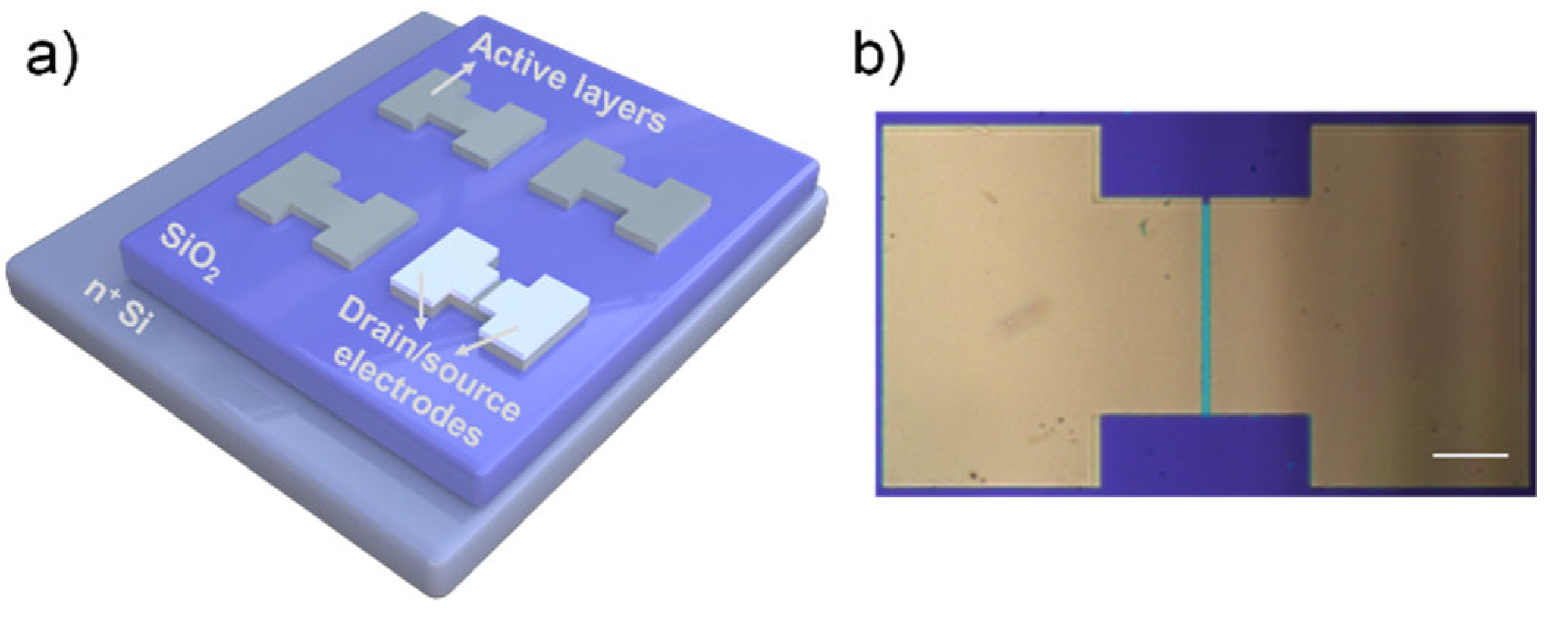
2.1. Preparation of TFT Devices

In this paper, Si/SiO2 (Si wafer with a thickness of 285 nm of SiO2 from HEFEI KEJING Materials Tech Co., Ltd., Hefei, China) slices were used as the bottom-gate electrode and dielectric layer. The Si/SiO2 sheets were cut into squares of size ~15 mm, which were, respectively, put into acetone, alcohol, and deionized water for ultrasonic cleaning for 10 min, and finally dried with nitrogen. AZO (2:98 wt %) and ZnO monolayer or double-layers structures were deposited on Si/SiO2 substrate by magnetron sputtering for 10 min. The growth conditions were set to a growth pressure of 8 mTorr, sputtering power of 100 W, and flow ratio of argon to oxygen 95:5.
The substrate prepared with the active layer was placed in the gel homogenizer; the rotation speed and the duration were set at 3000 r/min and 30 s, respectively. Then, the photoresist was uniformly applied on the surface of the substrate. After that, the substrate was placed on a hot plate heated at 90 °C for 5 min, and the substrate was fixed on the patterned mask of the active layer for the first exposure. The UV radiation intensity and the exposure time were set to 420 mW/cm2 and 4 s, respectively. Additionally, the photoresist reacted with UV light was washed with 0.5% NaOH after the exposure, and the graphics were developed. The source and drain electrodes were formed by evaporation of aluminum metal via an electron beam evaporation system. The substrate heating temperature was set to 60 °C, and the thickness of electrodes was 50 nm. The channel length and width of all TFT devices were about 10 μm and 300 μm, respectively. A TFT device with metal oxide active layers and the structure consisting of bottom gate and top contact was constructed as shown in Figure 1. Then, the prepared samples were annealed to 200 °C for 5 min at a heating rate of 5 °C/s with different annealing atmospheres in a rapid annealing furnace. The annealing pressure of TFT devices under a vacuum environment was 0.5 hPa. The samples were removed from furnace at room temperature after annealing. The Ion/Ioff and VT were estimated by extrapolating the linear portion of the (drain current (ISD))1/2 versus gate voltage (VG) curves at drain-source voltage (VSD) value of 20 V for all TFT devices.

2.2. Characterization

The active layers were prepared by rf magnetron sputtering (PVD75, Kurt. J. Lesker Company, Jefferson Hills, PA, USA). The electrodes and channel layers are graphically etched with a photolithography system (ABM/6/350/NUV/DCCD/M, ABM, Inc., San Francisco, CA, USA). The field effect characterizations were measured by a semiconductor parameter measuring instrument (B1500A, Keysight Technologies, Colorado Springs, CO, USA). The samples were annealed in different atmospheres using a vacuum rapid annealing furnace (RTP-100, UniTemp, Pfaffenhofen an der Ilm, Germany).

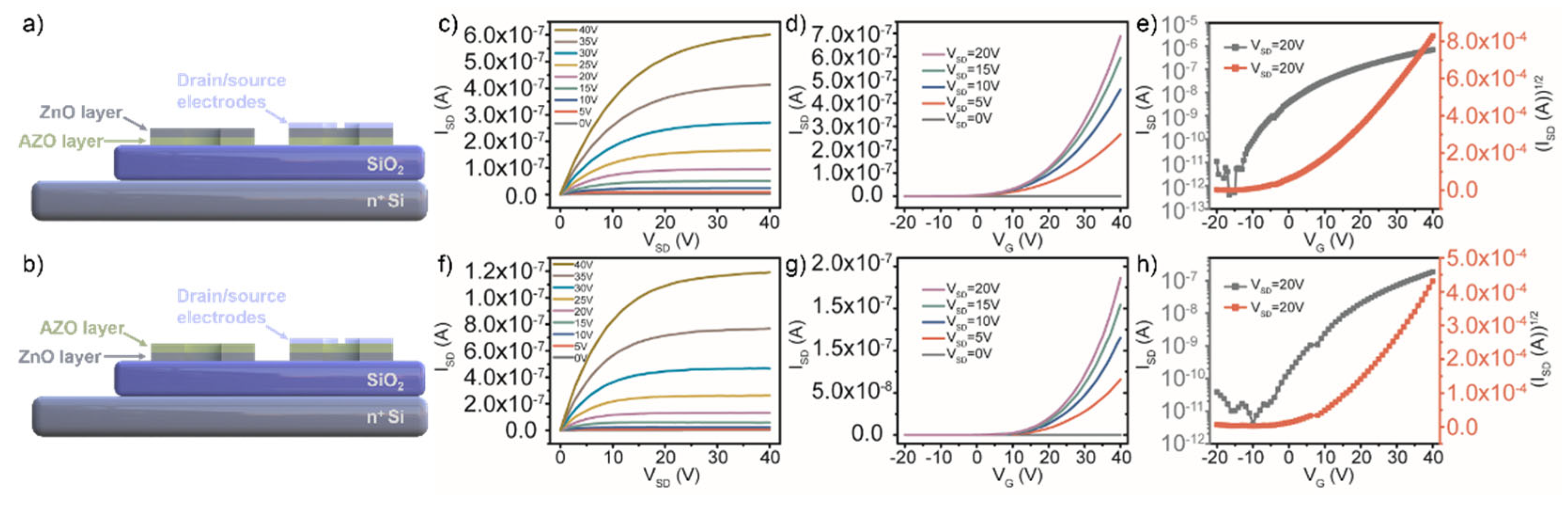
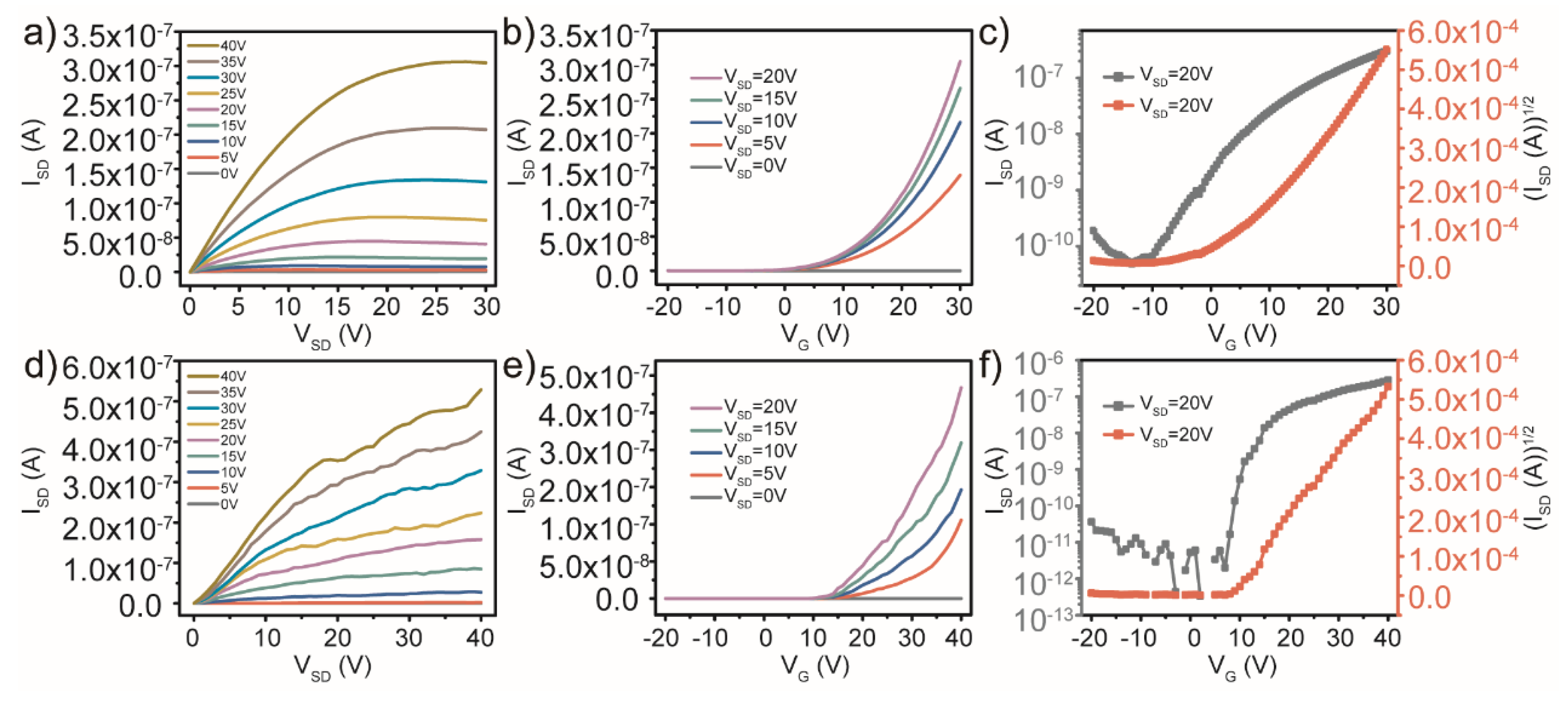
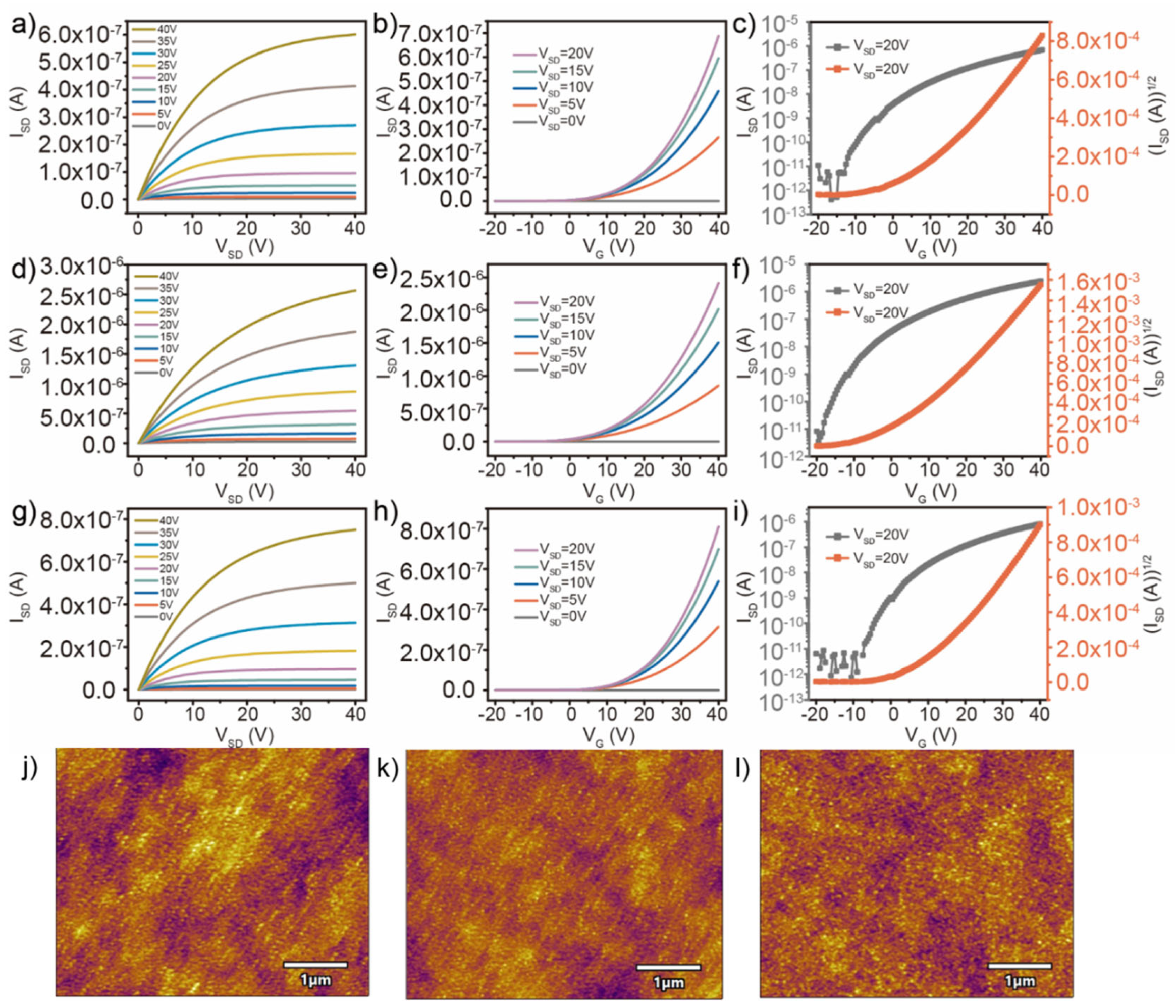
3. Results and Discussion

The double-active-layers of ZnO and AZO layers were deposited on the Si/SiO2 substrate by magnetron sputtering; then, patterned channel layers and source leakage electrodes were obtained by lithography. The channel length and width of all TFT devices were about 10 μm and 300 μm, respectively. The deposition sequence of AZO with a higher doping concentration and ZnO with few impurity-scattering centers and more stability was modulated to verify the performance of double-active-layers TFT devices. The double-active-layers with the thickness of 32 ± 0.5 nm was formed by a 5 min deposition of each single-layer, either by preparing the AZO layer first and then the ZnO layer (ZnO/AZO/SiO2/Si) or by reversing the deposition sequence (AZO/ZnO/SiO2/Si), as shown in Figure 2a,b. Figure 2c,f show the drain current versus drain-source voltage (ISD-VSD) output characteristics of TFTs with ZnO/AZO/SiO2/Si and AZO/ZnO/SiO2/Si double-active-layers at VG from 0 to 40 V, respectively. The curves show the typical n-type field-effect electrical properties with the clear transition from linear to saturation behavior with different deposition sequences of the channel layers. Figure 2d,g plot the typical transfer curves of these two TFT devices at different VSD from 0 to 20 V. As shown in Figure 2e,h, the Ion/Ioff and the VT estimated by extrapolating the linear portion of the (ISD)1/2 versus VG curves at VSD = 20 V of the two TFT devices with a double-active-layer structure can be calculated. The TFT with ZnO/AZO/SiO2/Si double-active-layers exhibited a VT of 9.5 V, a field-effect mobility of 0.0040 cm2/Vs, and an Ion/Ioff of 6.3 × 10⁴. In contrast, the device with AZO/ZnO/SiO2/Si double-active-layers showed lower electrical performance, including a VT of 14.3 V, a field-effect mobility of 0.0014 cm2/Vs, and an Ion/Ioff of 2.5 × 10⁴. The reason is that the AZO layer with more carrier concentration close to the insulation layer in devices can facilitate the regulation of more induced charges and obtain a lower operating voltage, thus reducing the power consumption of the TFT devices. In addition, the relatively stable ZnO layer can effectively ensure that the device has a lower off-state current. In addition, the subthreshold slopes (SS) of the TFT devices with ZnO/AZO/SiO2/Si and AZO/ZnO/SiO2/Si double-active-layers were 1.59 and 1.69 V/decade, respectively. The smaller SS value means that the ZnO/AZO/SiO2/Si TFTs switch from the off-state to the on-state more quickly and require a smaller voltage change.
For better verification, the TFT devices with a single-active-layer of AZO and AZO deposited for 10 min (~32 ± 0.5 nm thickness) were compared with the double-active-layers device. The output characteristics and transfer characteristics of single-active-layer TFT devices are plotted in Figure 3. As shown in Figure 3a, the transition from the linear to the saturation regime and a good regulating effect on the ISD are observable in the output characteristics of the TFTs with AZO single-active-layer under different VG. However, according to the performance of TFT devices derived from the transfer characteristics in Figure 3b,c, the value of Ion/Ioff of 4.7 × 10³ was relatively low. We know that the Ion/Ioff value determines the degree of antinoise signal interference of TFT devices. The reason is that the single-layer AZO with higher carrier concentration as the active layer makes the TFT device retain a higher off-state current. The field-effect mobility was also reduced to 0.0029 cm2/Vs by the introduction of more carrier scattering centers. However, the TFT device with a single-layer ZnO without other metal cations as an active layer does not exhibit the hard saturation and current regulation effects in the output characteristic and transfer characteristic curves, as shown in Figure 3d–f. Considering integral electrical performance of devices, the double-active-layers ZnO/AZO/SiO2/Si TFTs were elected for following optimization and discussion due to the higher Ion/Ioff and field-effect mobility.
The deposition conditions of both single- and double-active-layers discussed above were all completed at room temperature. Annealing treatment was required to release stress effects caused by atomic stacking in the channel layers. In order to avoid the gathering of functional groups on the surface of channel layers during the annealing process, the electrical properties of the double-active-layers ZnO/AZO/SiO2/Si TFTs before and after 5 min annealing at 200 °C in a vacuum environment and air atmosphere are compared in Figure 4. As shown in Figure 4d, the TFTs after vacuum annealing exhibit a good current regulation ability. In addition, it was found that the ISD value was larger than that of nonannealed samples under the same VG, which was due to the improved carrier mobility caused by the decrease in defects and the increase in regulated carrier concentration in conductive channels. The field-effect performance, including a VT of 2.9 V, a field-effect mobility of 0.010 cm2/Vs, and an Ion/Ioff of 6.8 × 10⁵ derived from the transfer characteristics, was significantly improved compared with the TFT devices before vacuum annealing treatment. In contrast, the field-effect performance, including a VT of 9.1 V, a field-effect mobility of 0.0043 cm2/Vs, and an Ion/Ioff of 1.4 × 10⁵ of the device after annealing in air atmosphere, was not significantly improved compared with that before annealing, as shown in Figure 4i. Although the stress defects in active layers were improved, the adsorption of functional groups on the channel surface will lead to the creation of acceptor-like surface states [38]. So, vacuum annealing can avoid introducing excessive surface defects to affect the TFT device performance. Furthermore, an annealing treatment can effectively increase the surface particle size and reduce the surface roughness so as to improve the scattering problem during carrier injection and migration. The variation of the double-active-layer ZnO/AZO/SiO2/Si surface roughness before and after annealing in a vacuum environment and air was analyzed by atomic force microscope in Figure 4j–l. The surface roughness of the ZnO/AZO channel layers without annealing treatment was 1.183 nm, and the roughness of the double-active layers was decreased to 0.913 nm and 1.057 nm after annealing in a vacuum environment and air, respectively. The reduction of interface roughness can further improve the electrical transport properties of TFTs. Finally, the field-effect parameters of the TFT devices with various active layers and annealing atmosphere are summarized in Table 1

4. Conclusions

We investigated a double-active-layers TFT device with a bottom-gate and top-contact (drain/source electrodes) structure and discussed the effect of different double-active-layers stacking modes on TFT properties and the advantages over a comparable device with a single-active-layer. The ZnO/AZO/SiO2/Si double layers had the advantage of higher carrier concentration and lower off-state current, which improved the regulation ability of ISD in the conductive channel of TFT devices. In addition, we introduced vacuum annealing treatment to improve the stress defects caused by atomic packing and to enhance the field-effect performance of the device. The optimized double-active-layers TFT exhibited a VT of 2.9 V, a field-effect mobility of 0.010 cm2/Vs, and an Ion/Ioff of 6.8 × 10⁵. However, compared with the full-fledged devices, this ZnO/AZO/SiO2/Si TFT still has a certain gap in the field-effect performance. In the next step, we will improve the electrical properties by improving and modifying the interface contact quality between the double-active-layers.

Author Contributions

Conceptualization, X.Y. (Xingzhen Yan) and K.S.; methodology, X.Y. (Xingzhen Yan) and K.S.; formal analysis, K.S., Y.Z. and B.L.; investigation, Y.W., F.Y. and C.W.; writing—original draft preparation, X.Y. (Xingzhen Yan) and K.S; writing—review and editing, X.Y. (Xingzhen Yan) and X.Y. (Xiaotian Yang); project administration, Y.C. and X.Y. (Xiaotian Yang); funding acquisition, X.Y. (Xingzhen Yan). All authors have read and agreed to the published version of the manuscript.

Funding

This research was funded by the Science and Technology Development Project of Jilin Province, China (Nos.YDZJ202201ZYTS396 and JJKH20220271KJ).

Conflicts of Interest

The authors declare no conflict of interest.

References

  1. Nomura, K.; Ohta, H.; Ueda, K.; Kamiya, T.; Hirano, M.; Hosono, H. Thin-film transistor fabricated in single-crystalline transparent oxide semiconductor. Science 2003, 300, 1269–1272. [Google Scholar] [CrossRef] [PubMed]
  2. Gelinck, G.; Huitema, H.; Veenendaal, E.; Cantatore, E.; Schrijnemakers, L.; Putten, J.; Geuns, T.; Beenhakkers, M.; Giesbers, J.; Huisman, B.; et al. Flexible active-matrix displays and shift registers based on solution-processed organic transistors. Nat. Mater. 2004, 3, 106–110. [Google Scholar] [CrossRef] [PubMed]
  3. Street, R.A. Thin-film transistors. Adv. Mater. 2009, 21, 2007–2022. [Google Scholar] [CrossRef]
  4. Hoffman, R.L.; Norris, B.J.; Wager, J.F. ZnO-based transparent thin-film transistors. Appl. Phys. Lett. 2003, 82, 733–735. [Google Scholar] [CrossRef]
  5. Fortunato, E.; Barquinha, P.; Pimentel, A.; Goncalves, A.; Marque, A.; Pereira, L.; Martins, R. Wide-Bandgap High-Mobility ZnO Thin-Film Transistors Produced at Room Temperature. Appl. Phys. Lett. 2004, 85, 2541–2543. [Google Scholar] [CrossRef]
  6. Dimitrakopoulos, C.D.; Purushothaman, S.; Kymissis, J.; Callegari, A.; Shaw, J.M. Low-Voltage Organic Transistors on Plastic Comprising High-Dielectric Constant Gate Insulators. Science 1999, 283, 822–824. [Google Scholar] [CrossRef]
  7. Crone, B.; Dodabalapur, A.; Lin, Y.Y.; Filas, R.W.; Bao, Z.; LaDuca, A.; Sarpeshkar, R.; Katz, H.E.; Li, W. Large-Scale Complementary Integrated Circuits based on Organic Transistors. Nature 2000, 403, 521–523. [Google Scholar] [CrossRef]
  8. Yuan, Y.; Giri, G.; Ayzner, A.L.; Zoombelt, A.P.; Mannsfeld, S.C.; Chen, J.; Nordlund, D.; Toney, M.F.; Huang, J.; Bao, Z. Ultra-high mobility transparent organic thin film transistors grown by an off-centre spin-coating method. Nat. Commun. 2014, 5, 3005. [Google Scholar] [CrossRef] [PubMed] [Green Version]
  9. Guo, E.; Xing, S.; Dollinger, F.; Hubner, R.; Wang, S.J.; Wu, Z.; Leo, K.; Kleemann, H. Integrated complementary inverters and ring oscillators based on vertical-channel dual-base organic thin-film transistors. Nat. Electron. 2021, 4, 588–594. [Google Scholar] [CrossRef]
  10. Nomura, K.; Ohta, H.; Takagi, A.; Kamiya, T.; Hirano, M.; Hosono, H. Room-Temperature Fabrication of Transparent Flexible Thin-Film Transistors Using Amorphous Oxide Semiconductors. Nature 2004, 432, 488–492. [Google Scholar] [CrossRef]
  11. Fortunato, E.; Barquinha, P.; Martins, R. Oxide Semiconductor Thin-Film Transistors: A Review of Recent Advances. Adv. Mater. 2012, 24, 2945–2986. [Google Scholar] [CrossRef] [PubMed]
  12. Banger, K.K.; Yamashita, Y.; Mori, K.; Peterson, R.L.; Leedham, T.; Rickard, J.; Sirringhaus, H. Low-temperature, high-performance solution-processed metal oxide thin-film transistors formed by a ‘sol–gel on chip’ process. Nat. Mater. 2011, 10, 45–50. [Google Scholar] [CrossRef] [PubMed]
  13. Islam, M.M.; Saha, J.K.; Hasan, M.M.; Kim, J.; Bukke, R.N.; Ali, A.; Jang, J. Spray-Pyrolyzed High-k Zirconium-Aluminum-Oxide Dielectric for High Performance Metal-Oxide Thin-Film Transistors for Low Power Displays. Adv. Mater. Interfaces 2021, 8, 2100600. [Google Scholar] [CrossRef]
  14. Ozer, E.; Kufel, J.; Myers, J.; Biggs, J.; Brown, G.; Rana, A.; Sou, A.; Ramsdale, C.; White, S. A hardwired machine learning processing engine fabricated with submicron metal-oxide thin-film transistors on a flexible substrate. Nat. Electron. 2020, 3, 419–425. [Google Scholar] [CrossRef]
  15. Kuribara, K.; Wang, H.; Uchiyama, N.; Fukuda, K.; Yokota, T.; Zschieschang, U.; Jaye, C.; Fischer, D.; Klauk, H.; Yamamoto, T.; et al. Organic transistors with high thermal stability for medical applications. Nat. Commun. 2012, 3, 723. [Google Scholar] [CrossRef] [PubMed] [Green Version]
  16. Rim, Y.S.; Chen, H.; Kou, X.; Duan, H.S.; Zhou, H.; Cai, M.; Kim, H.J.; Yang, Y. Boost Up Mobility of Solution-Processed Metal Oxide Thin-Film Transistors via Confining Structure on Electron Pathways. Adv. Mater. 2014, 26, 4273–4278. [Google Scholar] [CrossRef] [PubMed]
  17. Yarali, E.; Koutsiaki, C.; Faber, H.; Tetzner, K.; Yengel, E.; Patsalas, P.; Kalfagiannis, N.; Koutsogeorgis, D.C.; Anthopoulos, T.D. Recent Progress in Photonic Processing of Metal-Oxide Transistors. Adv. Funct. Mater. 2020, 30, 1906022. [Google Scholar] [CrossRef] [Green Version]
  18. Carcia, P.F.; McLean, R.S.; Reilly, M.H.; Nunes, G. Transparent ZnO thin-film transistor fabricated by rf magnetron sputtering. Appl. Phys. Lett. 2003, 82, 1117–1119. [Google Scholar] [CrossRef]
  19. Saha, J.K.; Billah, M.M.; Jang, J. Triple-Stack ZnO/AlZnO/YZnO Heterojunction Oxide Thin-Film Transistors by Spray Pyrolysis for High Mobility and Excellent Stability. ACS Appl. Mater. Interfaces 2021, 13, 37350–37362. [Google Scholar] [CrossRef]
  20. Hasan, M.M.; Bae, M.J.; Tokumitsu, E.; Chu, H.Y.; Kim, S.C.; Jang, J. High performance ferroelectric ZnO thin film transistor using AlOx/HfZrO/ZrOx gate insulator by spray pyrolysis. Appl. Phys. Lett. 2021, 119, 093502. [Google Scholar] [CrossRef]
  21. Yagliolu, B.; Yeom, H.Y.; Beresford, R.; Paine, D.C. High-mobility amorphous In2O3-10 wt% ZnO thin film transistors. Appl. Phys. Lett. 2006, 89, 062103. [Google Scholar] [CrossRef]
  22. Chiang, H.Q.; Wager, J.H.; Hoffman, R.L.; Jeong, J.; Keszler, D.A. High mobility thin-film transistors with amorphous zinc tin oxide channel layer. Appl. Phys. Lett. 2005, 86, 013503. [Google Scholar] [CrossRef]
  23. Jackson, W.B.; Hoffman, R.L.; Herman, G.S. High-performance flexible zinc tin oxide field-effect transistors. Appl. Phys. Lett. 2005, 87, 193503. [Google Scholar] [CrossRef]
  24. Jeong, S.; Ha, Y.G.; Moon, J.; Facchetti, A.; Marks, T.J. Role of Gallium Doping in Dramatically Lowering Amorphous-Oxide Processing Temperatures for Solution-Derived Indium Zinc Oxide Thin-Film Transistors. Adv. Mater. 2010, 22, 1346–1350. [Google Scholar] [CrossRef] [PubMed]
  25. Yabuta, H.; Sano, M.; Abe, K.; Aiba, T.; Den, T.; Kumomi, H.; Nomura, K.; Kamiya, T.; Hosono, H. High-mobility thin-film transistor with amorphous InGaZnO4 channel fabricated by room temperature rf-magnetron sputtering. Appl. Phys. Lett. 2006, 89, 112123. [Google Scholar] [CrossRef]
  26. Zhao, Y.; Wang, Z.; Xu, G.; Cai, L.; Han, T.H.; Zhang, A.; Wu, Q.; Wang, R.; Huang, T.; Cheng, P.; et al. High Performance Indium-Gallium-Zinc Oxide Thin Film Transistor via Interface Engineering. Adv. Funct. Mater. 2020, 30, 2003285. [Google Scholar] [CrossRef]
  27. Lee, M.; Jo, J.W.; Kim, Y.J.; Choi, S.; Kwon, S.M.; Jeon, S.P.; Facchetti, A.; Kim, Y.H.; Park, S.K. Corrugated Heterojunction Metal-Oxide Thin-Film Transistors with High Electron Mobility via Vertical Interface Manipulation. Adv. Mater. 2018, 30, 1804120. [Google Scholar] [CrossRef]
  28. Kumaran, S.; Liu, M.T.; Lee, K.Y.; Tai, Y. The Impact of Solvents on the Performances of Solution-Processed Indium Gallium Zinc Oxide Thin-Film Transistors Using Nitrate Ligands. Adv. Eng. Mater. 2020, 22, 1901053. [Google Scholar] [CrossRef]
  29. Ding, X.; Zhang, H.; Ding, H.; Zhang, J.; Huang, C.; Shi, W.; Li, J.; Jiang, X.; Zhang, Z. Growth of IZO/IGZO dual-active-layer for low-voltage-drive and high-mobility thin film transistors based on an ALD grown Al2O3 gate insulator. Superlattices Microstruct. 2014, 76, 156–162. [Google Scholar] [CrossRef]
  30. Kim, S.I.; Kim, C.J.; Park, J.C.; Song, I.; Kim, S.W.; Yin, H.; Lee, E.; Lee, J.C.; Park, Y. High Performance Oxide Thin Film Transistors with Double Active Layers. In Proceedings of the 2008 IEEE International Electron Devices Meeting, San Francisco, CA, USA, 15–17 December 2008; Volume 1, pp. 73–76. [Google Scholar] [CrossRef]
  31. Kim, D.J.; Kim, D.L.; Rim, Y.S.; Kim, C.H.; Jeong, W.H.; Lim, H.S.; Kim, H.J. Improved Electrical Performance of an Oxide Thin-Film Transistor Having Multistacked Active Layers Using a Solution Process. ACS Appl. Mater. Interfaces 2012, 4, 4001–4005. [Google Scholar] [CrossRef]
  32. Huo, W.; Liang, H.; Lu, Y.; Han, Z.; Zhu, R.; Sui, Y.; Wang, T.; Mei, Z. Dual-active-layer InGaZnO high-voltage thin-film transistors. Semicond. Sci. Technol. 2021, 36, 065021. [Google Scholar] [CrossRef]
  33. Kim, S.J.; Jeon, H.J.; Oh, S.J.; Lee, S.S.; Choi, Y.; Park, J.S.; Jeong, S. Formamide Mediated, Air-Brush Printable, Indium-Free Soluble Zn-Sn-O Semiconductors for Thin-Film Transistor Applications. ACS Appl. Mater. Interfaces 2014, 6, 18429–18434. [Google Scholar] [CrossRef] [PubMed]
  34. Liu, A.; Guo, Z.; Liu, G.; Zhu, C.; Zhu, H.; Shin, B.; Fortunato, E.; Martins, R.; Shan, F. Redox Chloride Elimination Reaction: Facile Solution Route for Indium-Free, Low-Voltage, and High-Performance Transistors. Adv. Electron. Mater. 2017, 3, 1600513. [Google Scholar] [CrossRef]
  35. He, Z.; Asare-Yeboah, K.; Zhang, Z.; Bi, S. Manipulate organic crystal morphology and charge transport. Org. Electron. 2022, 103, 106448. [Google Scholar] [CrossRef]
  36. He, Z.; Chen, J.; Li, D. Polymer additive controlled morphology for high performance organic thin film transistors. Soft Matter 2019, 15, 5790–5803. [Google Scholar] [CrossRef]
  37. Kamiya, T.; Hosono, H. Material characteristics and applications of transparent amorphous oxide semiconductors. NPG Asia Mater. 2010, 2, 15–22. [Google Scholar] [CrossRef] [Green Version]
  38. Hong, D.; Wager, J.F. Passivation of zinc-tin-oxide thin-film transistors. J. Vac. Sci. Technol. B 2005, 23, L25–L27. [Google Scholar] [CrossRef]
Figure 1. (a) Schematic diagram of fabrication of a metal oxide TFT device. (b) Microscope image of the channel pattern. The scale bar is 100 μm.
Micromachines 13 02024 g001
Figure 2. Schematic diagrams of cross-section structure of oxide TFTs with ZnO/AZO/SiO2/Si (a) and AZO/ZnO/SiO2/Si (b) double-active-layers. Output characteristics and transfer characteristics of TFTs with ZnO/AZO/SiO2/Si layers (ce) and with AZO/ZnO/SiO2/Si layers (fh).
Micromachines 13 02024 g002
Figure 3. Output characteristics and transfer characteristics of TFTs with AZO single-active-layer (ac) and with ZnO single-active-layer (df).
Micromachines 13 02024 g003
Figure 4. Output characteristics and transfer characteristics of TFTs with ZnO/AZO/SiO2/Si double-active-layers before (ac) and after annealing in vacuum environment (df) and in air (gi). Atomic force microscope images of the ZnO/AZO channel layers without (j) and with annealing treatment in vacuum environment (k) and in air (l).
Micromachines 13 02024 g004
Table 1. The field-effect parameters of the TFTs with various active layers and annealing atmosphere.
TypeThreshold Voltage (V)On/Off Ratio
AZO/ZnO/SiO2/Si14.32.5 × 104
ZnO/AZO/SiO2/Si9.56.3 × 104
After annealing in vacuum2.96.8 × 105
After annealing in air9.11.4 × 105
Publisher’s Note: MDPI stays neutral with regard to jurisdictional claims in published maps and institutional affiliations.

