Review

Recent Advances In Silicon Carbide Chemical Mechanical Polishing Technologies

1
Department of Photonics, Institute of Electro-Optical Engineering, National Yang Ming Chiao Tung University, Hsinchu 30010, Taiwan
2
Institute of Pioneer Semiconductor Innovation, Industry Academia Innovation School, National Yang Ming Chiao Tung University, Hsinchu 30010, Taiwan
3
Semiconductor Research Center, Hon Hai Research Institute, Taipei 11492, Taiwan
4
Department of Mechanical Engineering, National Taiwan University of Science and Technology, Taipei 10607, Taiwan
*
Authors to whom correspondence should be addressed.
Micromachines 2022, 13(10), 1752; https://doi.org/10.3390/mi13101752
Submission received: 30 August 2022 / Revised: 6 October 2022 / Accepted: 11 October 2022 / Published: 16 October 2022
(This article belongs to the Special Issue Ultra-Precision Manufacturing Technology)

Abstract

:
Chemical mechanical polishing (CMP) is a well-known technology that can produce surfaces with outstanding global planarization without subsurface damage. A good CMP process for Silicon Carbide (SiC) requires a balanced interaction between SiC surface oxidation and the oxide layer removal. The oxidants in the CMP slurry control the surface oxidation efficiency, while the polishing mechanical force comes from the abrasive particles in the CMP slurry and the pad asperity, which is attributed to the unique pad structure and diamond conditioning. To date, to obtain a high-quality as-CMP SiC wafer, the material removal rate (MRR) of SiC is only a few micrometers per hour, which leads to significantly high operation costs. In comparison, conventional Si CMP has the MRR of a few micrometers per minute. To increase the MRR, improving the oxidation efficiency of SiC is essential. The higher oxidation efficiency enables the higher mechanical forces, leading to a higher MRR with better surface quality. However, the disparity on the Si-face and C-face surfaces of 4H- or 6H-SiC wafers greatly increases the CMP design complexity. On the other hand, integrating hybrid energies into the CMP system has proven to be an effective approach to enhance oxidation efficiency. In this review paper, the SiC wafering steps and their purposes are discussed. A comparison among the three configurations of SiC CMP currently used in the industry is made. Moreover, recent advances in CMP and hybrid CMP technologies, such as Tribo-CMP, electro-CMP (ECMP), Fenton-ECMP, ultrasonic-ECMP, photocatalytic CMP (PCMP), sulfate-PCMP, gas-PCMP and Fenton-PCMP are reviewed, with emphasis on their oxidation behaviors and polishing performance. Finally, we raise the importance of post-CMP cleaning and make a summary of the various SiC CMP technologies discussed in this work.

1. Introduction

Silicon Carbide (SiC), a wide-bandgap semiconductor material, has attracted tremendous attention from both academics and industries in recent years. SiC possesses outstanding electrical properties for the power device application, including high breakdown electric field (2.5 × 10⁶ V cm−1), high thermal conductivity (5 W cm−1 K−1), high operating temperature (low intrinsic carrier concentration up to 900 °C) and high saturation drift velocity (2 × 107 cm s−1) [1]. Although there have been more than 250 polytypes of SiC reported, the most commonly used polytypes are 4H-SiC, 6H-SiC and 3C-SiC. In particular, 6H-SiC and 4H-SiC wafers with diameters up to 8 inches have already been commercialized. Following our previous review of the SiC MOSFET fabrication process [1], in this review article, we focus on the recent advances in chemical mechanical polishing (CMP) technologies, which aim to provide atomically flat and subsurface damage-free SiC substrates for high-quality epitaxy and high-performance power device fabrication. Given that SiC is well-known for its exceptionally high hardness, brittleness and inertness, the current CMP of SiC usually suffers from high machining costs and low throughput. A comprehensive review of current CMP technologies may pave the way for further investigation to attain more efficient and more cost-effective SiC CMP.
Nowadays, a typical production process from the SiC boule to SiC substrates includes cropping/blocking, creating flat/notch, slicing, edge grinding, laser marking, lapping, grinding, CMP, post-CMP cleaning, inspecting and packaging (Table 1). The lapping and grinding steps involve mechanical polishing by using a diamond abrasive slurry or a diamond grinding wheel. The following CMP can effectively remove the machinery marks and subsurface damages induced by the lapping and grinding steps. Particularly, the effectiveness of surface oxidation plays a critical role in the SiC CMP. Therefore, the oxidation behavior on the Si-face and C-face surfaces of a SiC wafer and how it affects the CMP efficiency will be discussed. Finally, a summary of the emerging hybrid CMP technologies will be made and the importance of post-CMP cleaning will be pointed out.

2. Various SiC CMP Technologies

Owing to the high hardness and high brittleness of SiC, diamond abrasives are commonly used in the lapping and grinding steps (Table 1). The resulting wafer surface topography, roughness and subsurface damage depth depend on the diamond abrasive size applied. In general, a smaller diamond abrasive size leads to a flatter surface, the smaller roughness and a shallower subsurface damage. The different levels of surface roughness and subsurface damage depth at different steps of the SiC wafer production process are illustrated in Figure 1. Compared to the lapping and grinding steps, since the hardness level decreases when the SiC surface gets oxidized, relatively soft and nanometer size abrasives, such as SiO2, Al2O3 and CeO2 nanobeads, are used during the CMP, resulting in angstrom scale flatness and subsurface damage free SiC surfaces. To date, for industrial applications, surface roughness (Ra) of Si-face < 0.1 nm and C-face < 0.4 nm are essential [2]. However, the relatively low-material-removal rate (MRR) remains the major issue of CMP. Compared to the MRR of Si CMP which is a few micrometers per minute, the current MRR of SiC CMP is only a few micrometers per hour. Therefore, how to optimize the process parameters and combine other energies into the system while maintaining acceptable surface quality has become the research focus of recent years.

2.1. SiC CMP

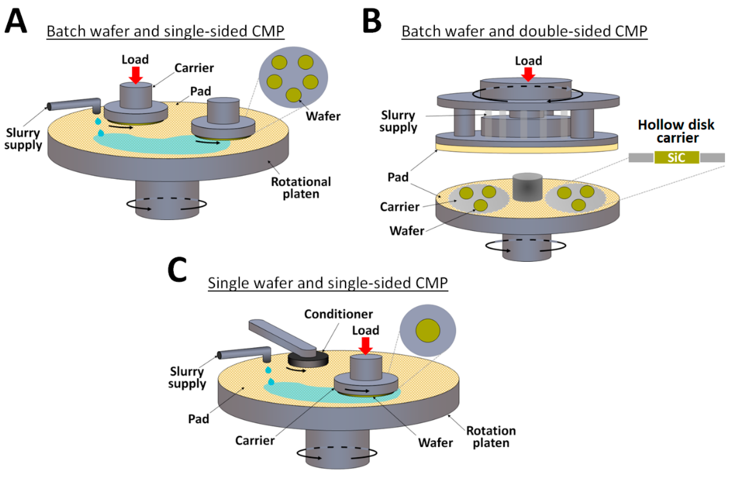
As the 100-mm, 150-mm and 200-mm SiC wafers are being commercialized for power device fabrication, the specifications of production-grade SiC wafers have become higher in order to meet the demand for more stable epitaxial growth. Three configurations of CMP have been developed to achieve higher MRR, lower surface roughness, less scratch and more uniform surface topography (Figure 2 and Table 2). For the batch wafer and single-sided CMP (Figure 2A), multiple wafers are loaded on the same polishing head by wax-mount or template-fix. For the batch wafer and double-sided CMP (Figure 2B), multiple wafers are loaded on the hollow disk carrier. Since there is no adhesive force between the wafer and carrier, the pressure and rotation speed are limited for preventing the wafers from slipping out, leading to relatively low MRR. For the single wafer and single-sided CMP (Figure 2C), the wafer tightly adheres to the polishing head by vacuum, allowing for higher pressure, higher rotation speed, and thus, higher MRR [2]. In practice, the double-sided CMP can serve as the first polishing step to polish the Si-face and C-face surfaces simultaneously. Since the C-face surface usually has a few times higher MRR than the Si-face surface, the single-sided CMP will continue to polish the Si-face surface until the production-grade level is achieved. Likewise, two single-sided CMP steps can be applied to, first, polish the Si-face and, then, the C-face for the graphene on C-face SiC application [4].
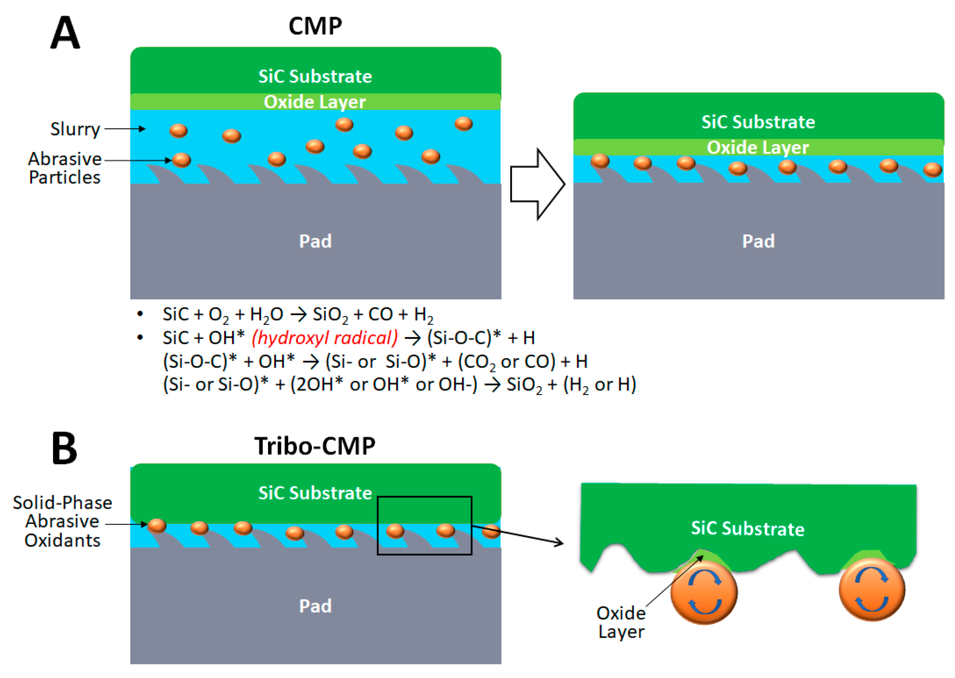
Oxidants in the slurry provide the chemical driving force in the CMP system, as they produce a softer oxidized surface which can be removed by abrasives in the slurry and the conditioned CMP pad simultaneously (Figure 3A). To achieve a balance between surface oxidation and oxide layer removal, it is critical to understand the chemical and mechanical properties of the Si-face and C-face surfaces. In 2019, Lu et al. found that it is harder to remove C-face than Si-face, as revealed by the nano-indentation and nano-scratching methods [5]. The critical indentation load (Pc) of the Si-face (2.3 mN) and C-face (1.5 mN) surfaces and the effective indentation modulus (Er) of the Si-face (387.51 GPa) and C-face (266.02 GPa) surfaces were obtained by the Oliver-Pharr method. The nano-scratching test with a constant load of 4 mN at 1 µm s−1 scratch velocity was performed. The friction coefficients of the Si-face and C-face surfaces were measured to be 0.1778 and 0.2176, respectively. Most importantly, the resulting MRRs on the 6H-SiC Si-face and C-face surfaces were equal to 6.13 nm m−1 and 13.94 nm m−1, respectively, indicating that C-face is indeed easier to remove than Si-face [5]. In 2022, Shi et al. investigated the mechanical properties of different crystal orientations on a polished 4H-SiC wafer by using the nano-indentation and nano-scratching methods [6]. It was found that a larger elastic modulus leads to less material deformation, and therefore, a harder characteristic. At the penetration depth of 1200 nm, the Si-face surface showed elastic modulus and hardness equal to 305.5 GPa and 29.77 GPa, respectively. In contrast, the C-face surface showed elastic modulus and hardness equal to 476.7 GPa and 37.62 GPa, respectively, at the same penetration depth. Furthermore, the residue depth of indentation was 12.22 nm on the Si-face and 25.67 nm on the C-face, indicating more elastic recovery on the Si-face [6].
The SiC oxidation rate is strongly dependent on the crystal orientation. In 2011, Nitta et al. reported 4H-SiC MRR of 62 nm h−1 and 34 nm h−1 by using hydrogen peroxide (H2O2) and periodic acid (H5IO6) as the oxidants in a pH 10 slurry environment, respectively [7]. If using colloidal silica slurry alone, the MRR was only 12 nm h−1. Furthermore, the MRR increased from 47 nm h−1 to 106 nm h−1 after adding amine (piperazine) into the mixture of H2O2 and colloidal silica slurry. Without the amine component in the slurry, the oxide layer, which is formed through the Si radicals or Si−O−C radicals on the SiC surface, was mechanically removed by colloidal silica. In contrast, with the amine additive, it became the active oxide layer composed of Si-amine complexes to be mechanically removed by colloidal silica [7]. In 2013, Pan et al. proposed another chemical reaction path between H2O2 and SiC [8]. The 6H-SiC MRR increased from 80 nm h−1 to 105 nm h−1 with the H2O2 concentration increased from 3 wt% to 6 wt%. Adding alkali into the existing slurry (6 wt% H2O2 and 30 wt% colloidal silica) allows more hydroxyl ions into the system to enhance the chemical reaction. The CMP results showed 120% and 56% MRR increases with 0.5 wt% KOH and 0.5 wt% MEA added into the slurry, respectively [8]. In 2017, Chen et al. analyzed the chemical composition at the 6H-SiC surface by using X-ray photoelectron spectroscopy (XPS) under the conditions of as-received, pre-polished, after dipping in KMnO4 solution and after dipping in KMnO4 and KOH solutions sequentially with varied pH values [9]. The significant decrease in Si-Ox-Cy and Si-O2 in the Si 2p spectra suggests native oxide removal from the as-received to pre-polish condition. Subsequently, the total oxide concentration increased dramatically after being dipped in KMnO4 solution and then decreased sharply after KOH treatment. The absence of the Si-O2 peak further confirms that the oxide layer can be dissolved in KOH [9].
In 2020, Tsai et al. proposed a mechanochemical CMP process (Tribo-CMP) [10]. In addition to the global oxidation taking place at the slurry and SiC interface, localized oxidation can also occur when the abrasive oxidants roll on the SiC wafer surface (Figure 3B). In this study, the water-dispersible abrasive oxidants composed of fullerene (C60) and β-cyclodextrin (β-CD) with particle sizes of 236 nm were used. During the CMP, the polishing pressure was 5.6 psi and the rotation speed was 90 rpm with a felt pad on the c-face. When using 0.01 wt% C60/β-CD abrasive oxidants in combination with 1 wt% 17-nm SiO2 particles, the resulting MRR was 49.9% higher than the control group, which only used 1 wt% 17-nm SiO2 particles. However, surface roughness (Sa) also increased around two fold for the test group, indicating the effect of non-uniform abrasion [10]. In 2021, Qi et al. investigated five solid-phase abrasive oxidants, including Na2CO3-1.5H2O2, KIO3, KClO3, KMnO4 and NaOH, for Tribo-CMP on 6H-SiC [11]. The SiC surface can be oxidized by oxygen generated from the decomposition of oxidants, along with friction-induced heat and water in the slurry formulation or ambient air. The solid-phase oxidants were sprayed on the polyurethane pad and the polishing experiments were conducted under the conditions of polishing pressure = 2 psi, polishing platen rotation speed = 60 rpm and polishing time = 90 min. A MRR of more than 1 µm h−1 can be consistently obtained for all five oxidants, but the resulting surface roughness was unsatisfactory. Meanwhile, obvious surface scratches and pits can be found under SEM inspection [11]. In addition to the solid-phase abrasive oxidants described above, in 2021, Ni et al. applied synthetic SiO2/CeO2 abrasives for CMP on the Si-face surface, under the conditions of polishing pressure = 3.5 psi and rotation speed = 90 rpm with a polyurethane pad [12]. The MRR equal to 0.451 µm h−1, 1.207 µm h−1 and 1.258 µm h−1 and the surface roughness (Ra) equal to 0.227 nm, 0.216 nm and 0.242 nm were obtained for the SiO2, SiO2/CeO2 and CeO2 abrasives, respectively. This result indicates that the synthetic SiO2/CeO2 abrasives with softer SiO2 cores (particle size: 80 nm to 90 nm) and harder CeO2 shells (shell thickness: 10 nm to 30 nm) not only generate a smaller surface roughness than pure CeO2 abrasives, but also provide a connection path to oxidized wafer surface through the Ce-O-Si bonds, which increases the sheer force during the CMP process [12].
The electrostatic interaction between the SiC wafer and abrasive particles is another critical factor to obtain an atomically flat surface with high MRR. Within a certain slurry pH range, the abrasive particles electrostatically adhere to the SiC wafer surface. Although the attached particles can provide a consistent mechanical force to remove the oxide layer, it might affect the oxidation efficiency if the particles remain at the same position and cannot be removed by the pad asperity. On the contrary, when the abrasive particles are electrostatically repelled away from the SiC wafer surface, the chance of having defects becomes higher and the MRR becomes lower, thus, requiring more concentrated slurry to achieve comparable polishing results. In 2007, Singh et al. determined that the iso-electric point (IEP) of SiC in deionized water is 5 [13]. Therefore, SiC carries a positive zeta-potential at a pH lower than the IEP. However, the IEP might shift to 3.6 when adding dispersant into deionized water, indicating that the IEP of SiC varies with the slurry composition. In 2015, Chen et al. investigated how the zeta-potential of potassium permanganate influences the performance of CMP based on SiO2 and CeO2 slurry particles [14]. Positive zeta-potentials were obtained for the pH range from 2 to 8 in the CeO2-based slurry, but there was no positive zeta-potential observed in the SiO2-based slurry for the pH range from 2 to 10. Under the conditions of polishing pressure = 4 psi, rotation speed = 90 rpm and potassium permanganate slurry pH = 2, the MRR and surface roughness (Ra) on the Si-face surface of 6H-SiC were measured to be 1.089 µm h−1 and 0.11 nm, respectively, when the polyurethane pad and CeO2 abrasives were used. Chen et al. further explained that abrasive particles with negative surface charges would easily attach to the SiC wafer surface. The attached abrasive particles then formed a blocking layer during the surface oxidation process, thus, lowering the MRR [14]. In 2021, Wang et al. demonstrated a high MRR of 1.4 µm h−1 with surface roughness (Ra) of 0.105 nm on the Si-face surface of 4H-SiC, by using an Al2O3 abrasive-based potassium permanganate slurry with pH = 2 [15]. The experiment was conducted under the conditions of polishing pressure = 6 psi and rotation speed = 90 rpm. However, the MRR continuously decreased to 1.1 µm h−1 when the pH increased to 12. The surface roughness (Ra) can be further improved from 0.105 nm to 0.066 nm after the second polishing step using the slurry composed of H2O2 oxidant, V2O5 catalyst and SiO2 abrasive [15]. It is worth noting that the electrostatic interaction plays a critical role not only at the wafer and abrasives interface, but also in the dispersion of abrasive particles. The optimization of abrasive particle size distribution in the slurry can effectively lower the surface scratches [16].
Compared to the commonly used liquid abrasive slurry, the fixed abrasive CMP technique provides higher mechanical force for higher MRR. In 2022, Wang et al. investigated non-aqueous slurries based on various types of organic solvents, such as methanol, ethanol, ethylene glycol and glycerol, with an abrasive pad fixed with self-sharpening and agglomerated diamonds (particle size: 3 µm to 5 µm) [17]. Under the conditions of polishing pressure = 0.7 psi and rotation speed = 50 rpm, the ethanol test group shows the highest MRR equal to 14.38 µm h−1. Meanwhile, the methanol test group shows the lowest surface roughness (Sa) equal to 12.22 nm, which however, is still worse than typical SiC performance [17]. In 2021, Zhou et al. applied molecular dynamics to simulate the surface morphology, subsurface damage and temperature distribution in a fixed abrasive CMP environment [18]. It was found that high-quality CMP requires uniform abrasive sizes and frequent interactions among neighboring abrasives [18]. On the other hand, a semi-fixed abrasive can be another technique to achieve higher MRR with lower surface roughness. In 2015, Lu et al. fabricated a semi-fixed abrasive sol-gel (SG) CMP pad, which can resolve the issue of uneven particle protrusion [19]. By using biopolymers as the matrix material, abrasives can be semi-fixed and self-adjusted to the same datum plan when the pad touches the wafer surface. As a result, the surface roughness (Ra) was greatly improved to 1.79 nm. In contrast, if using a fixed abrasive CMP pad, the surface roughness (Ra) was 24.61 nm [19]. Following a similar concept, in 2022, Luo at el. proposed that the semi-fixed SG CMP pad based on SiO2-modified diamonds, which are considered as soft–hard mixed abrasives, can further reduce the surface damage of the SiC substrate [20].
In addition to the experimental works, in 2022, Kayanuma et al. applied the density functional theory (DFT), unrestricted B3LYP method and 6-31G(d) basis set to analyze the reaction between OH radicals and O atoms within 10 surfaces of Si and C atoms on both Si-face and C-face surfaces [21]. The calculation results show that Si-O-Si bonds are formed on the Si-face and C-O-Si bonds are formed on the C-face, indicating that the Si-C bonds on the C-face can be easily dissociated by OH radicals to form a softer and easier machine surface [21]. In 2022, Morishita et al. analyzed the reactions involving water and H2O2 on the Si-face and C-face surfaces of 2H-SiC by using an ab initio molecular dynamics (AIMD) simulation [22]. The simulation results indicated that the C-face has a higher oxidation rate than the Si-face when either water or H2O2 was used because the Si-face is saturated with hydroxyl or hydrogen groups in a very short time. The higher oxidation rate leads to a higher MRR during the CMP process [22].
In summary, the three SiC CMP configurations currently used in the industry are introduced and the significance of process integration is highlighted. Furthermore, the mechanical properties and oxidation behaviors on the Si-face and C-face surfaces are compared. We also raise the importance of electrostatic interaction and how it affects CMP efficiency. As pointed out in the literature [23], integrating hybrid energies into the CMP system can be an effective approach to enhance oxidation efficiency as well as MRR. Therefore, in the following sections, we focus on recent advances in electro-CMP (ECMP) and photocatalyzed-CMP (PCMP) and their variants, such as Fenton-ECMP, ultrasonic-ECMP, sulfate-PCMP, gas-PCMP and Fenton-PCMP.

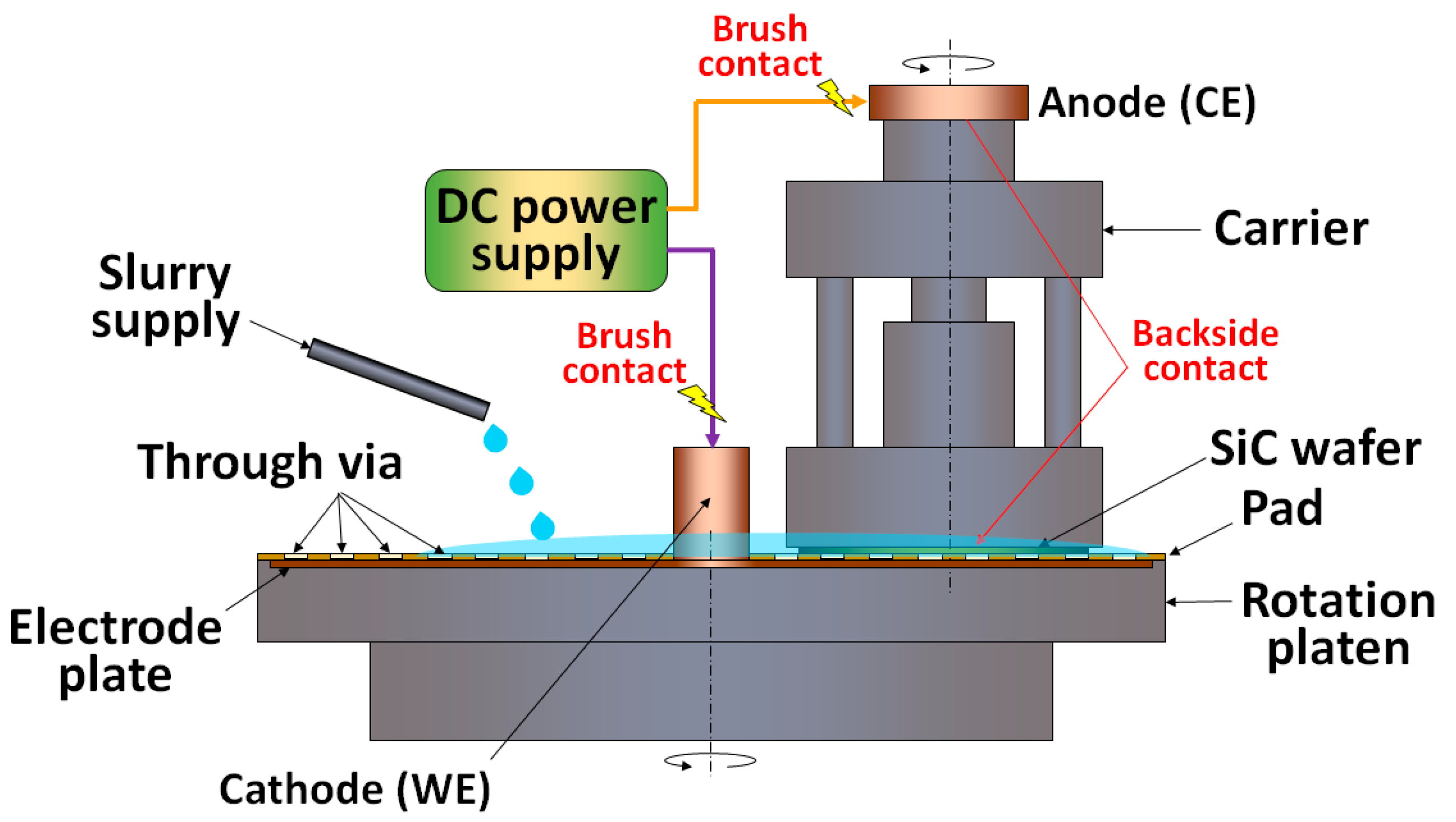
2.2. SiC Electro-CMP (ECMP)

The electro-CMP (ECMP) process has been widely investigated for the CMP of metal layers, such as Cu, W and Al, for many years [24]. For the SiC ECMP, the anodic oxidation can convert the hard SiC surface into a softer oxide layer, so that the abrasives composed of CeO2 or SiO2 can efficiently remove the oxide layer. In a typical ECMP setup (Figure 4), a working electrode (WE) is connected to a copper plate which has direct contact with the SiC wafer. A counter electrode (CE) is connected to the slip ring of the spindle and a reference electrode (RE) is connected to an Ag/AgCl plate. Since the ECMP relies on the wafer conductivity, N-type SiC wafers with low resistivity (~10−3 Ω·cm) are usually preferable to semi-insulating SiC wafers with high resistivity (~106 Ω·cm).
The potential dynamic polarization curve (PD curve) is often used to define the active region, passive region, transient region and trans-passive region, which can be used as references for setting the voltage range of ECMP. In 2019, Chen et al. analyzed the PD curves and found that there’s no clear passive region of 4H-SiC in different alkaline solutions [25]. On the other hand, the oxide layer thicknesses on both Si-face and C-face surfaces became thicker when higher voltages were applied to the 20 wt% NaNO3 solution. Furthermore, the C-face surface showed a significantly higher oxidation degree than the Si-face surface, and the difference increased with the larger voltage applied. By using nanoindentation tester, the hardness of Si-face decreased from 41.18 GPa to 2.53 GPa, and the hardness of C-face decreased from 32.1 GPa to 3.01 GPa after oxidation [25]. In 2015, Deng et al. compared the performance of diamond abrasive and CeO2 abrasive on an ECMP platform with 4H-SiC [26]. Under the conditions of polishing pressure = 3.74 kPa and rotation speed = 2000 rpm, a scratch-free surface was obtained by using CeO2 abrasive particles with a particle diameter of 190 nm. From the nanoindentation test, the surface hardness decreased from 34.5 GPa to 1.9 GPa after the anodic oxidation. The oxide layer growth rate was highly dependent on the applied voltage and the initial wafer surface roughness. For example, the oxide layer growth rates were equal to 0.6 µm h−1 and 0.92 µm h−1 when the applied voltages were equal to 5 V and 10 V, respectively. An oxide layer growth rate equal to 7.93 µm h−1 can be obtained on the diamond abrasive polished surface, which however, contained a subsurface damage layer [26].
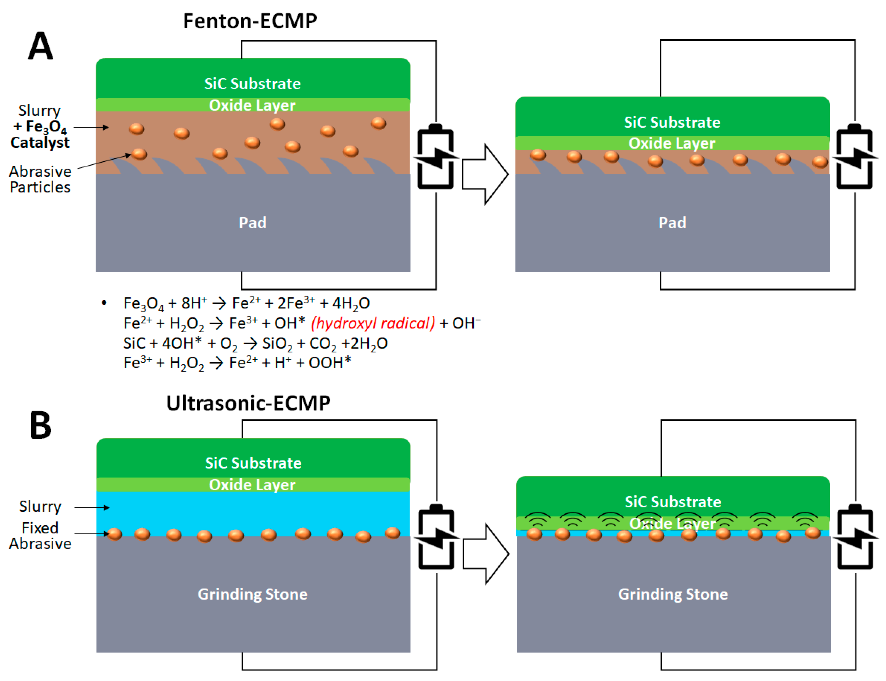
In 2020, Deng et al. proposed that more hydroxyl radicals can be generated by the Fenton reaction, enhancing the oxidation of SiC CMP, during which ferrosoferric oxide (Fe3O4) is used as the catalyst [27]. The process is often called Fenton-ECMP (Figure 5A). In addition, in 2021, Deng et al. further studied the contribution of the Fenton reaction to the ECMP process [28]. Based on the oxidation activity on the C-face surface, the hydroxyl concentration increased by 196.24% and 135.03% when applying 3 V into the 2 wt% Fe3O4 and 5 wt% H2O2 slurry and 3 V into the 2 wt% Fe3O4 and 7.5 wt% H2O2 slurry, respectively. The hydroxyl concentration increased by 26.88% when the applied voltage was increased from 1.5 V to 3 V with the 2 wt% Fe3O4 and 5 wt% H2O2 slurry. Under the conditions of polish pressure = 0.04 MPa, rotation speed = 60 rpm, slurry flow rate = 30 mL min−1 and using a polyurethane pad, the MRR increased by 65.59% (from 238.36 nm h−1 to 394.7 nm h−1) and by 57.27% (from 281.93 nm h−1 to 443.4 nm h−1) after applying 1.5 V and 3 V into the 2 wt% Fe3O4 and 7.5 wt% H2O2 slurry, respectively. The initial wafer surface roughness (Ra) was 181.33 nm and then reduced to 31 nm to 36 nm by using the Fenton-ECMP. The lowest surface roughness (Ra) of 31.103 nm was achieved by applying 3 V into the 2 wt% Fe3O4 and 7.5 wt% H2O2 slurry [28].
In 2021, Yang et al. demonstrated a three-step ECMP process, which can potentially produce epitaxy-ready wafers directly from as-sliced wafers [29]. First, #8000 diamond fixed abrasive grinding stone (abrasive size: 1 µm) was used for ECMP at a current density of 20 mA cm−2 for 20 min to achieve MRR equal to 62 µm h−1, while decreasing the surface roughness (Sq) from 163.33 nm to 25.45 nm. Second, apply a #8000 CeO2 fixed abrasive grinding stone (abrasive size: 1 µm) at the current density of 10 mA cm−2 for 30 min to obtain 11 µm h−1 MRR and decrease surface roughness (Sq) to 0.82 nm. Finally, using the same #8000 CeO2 fixed abrasive grinding stone (abrasive size: 1 µm) at a passivation potential of 3 V for 1 h to achieve 6.3 µm h−1 MRR and decrease surface roughness (Sq) to 0.11 nm. A scratch-free and subsurface damage=free surface can be obtained, as confirmed by scanning white-light interferometry (SWLI) images and Raman images, respectively [29]. In 2022, Yang et al. proposed a slurry-less ultrasonic vibration-assisted ECMP (ultrasonic-ECMP) by placing a vibrator onto the lower polishing plate (Figure 5B) [30]. The working principle is based on the anodic oxidation of SiC, followed by the oxide layer removal by a fixed abrasive grinding stone. Under the conditions of polishing pressure = 30 kPa, wafer rotation speed = 50 rpm, platen rotation speed = 200 rpm, grinding stone oscillation rate = 2 mm s−1, ultrasonic vibration frequency = 35 kHz, ultrasonic vibration power = 500 W and voltage applied into the 1 wt% NaCl electrolyte = 25 V, the resulting MRR was equal to 14.54 µm h−1, which is significantly higher than the conventional CMP (0.05 µm h−1) and ECMP (3.2 µm h−1). Despite the high MRR, obvious surface roughness can be found on the wafer surface after the ultrasonic-ECMP process. For comparison, the wafer surface roughness (Sq) of ECMP and ultrasonic-ECMP treated wafers was 0.528 nm and 1.993 nm, respectively. The results raise the importance of vibration amplitude optimization in different electrolytes, which leads to different oxidation behaviors [30].
In summary, although the ECMP technologies have the limitation of being only suitable for N-type SiC wafers, compared to the conventional CMP described in the previous section, the ECMP technologies provide the potential to double-sided polishing which can increase the MRR due to higher incoming surface roughness from the mechanical polishing step. Furthermore, after the anodic oxidation, similar surface hardness levels on the Si-face and C-face surfaces may lead to similar MRRs, facilitating the CMP process integration in the future.

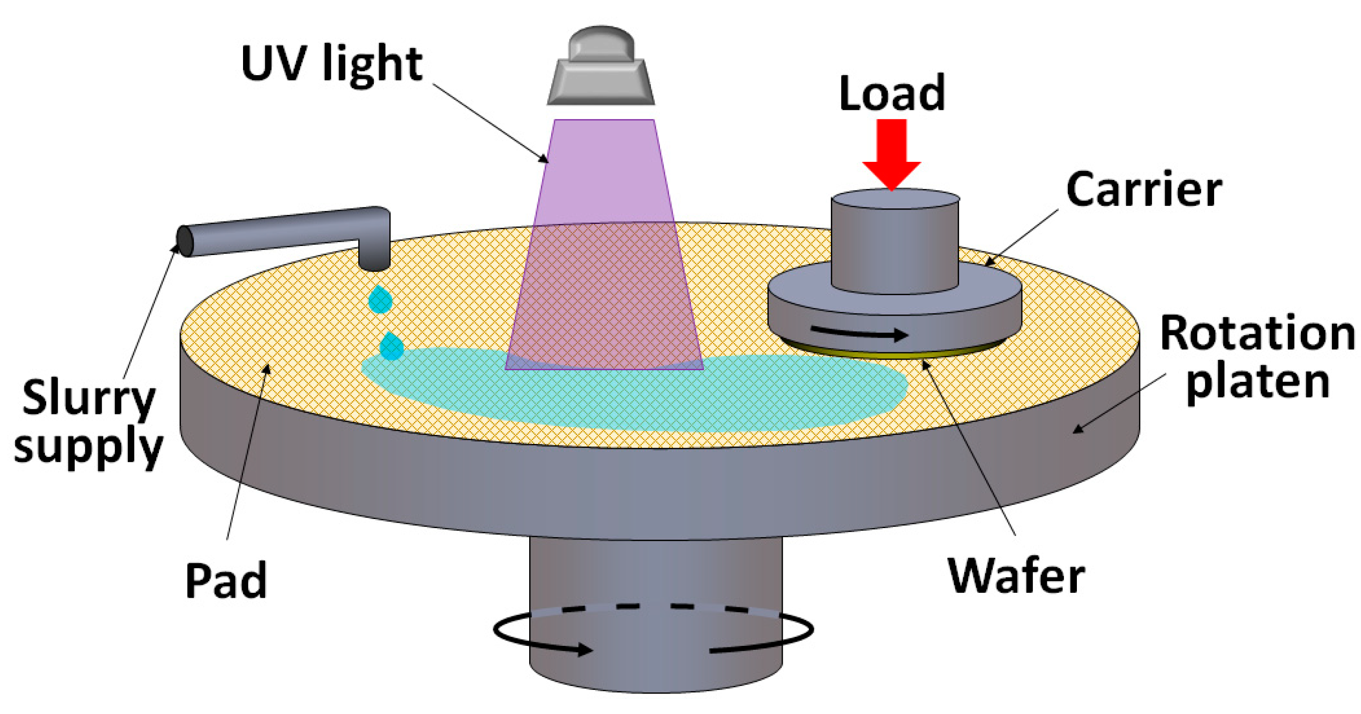
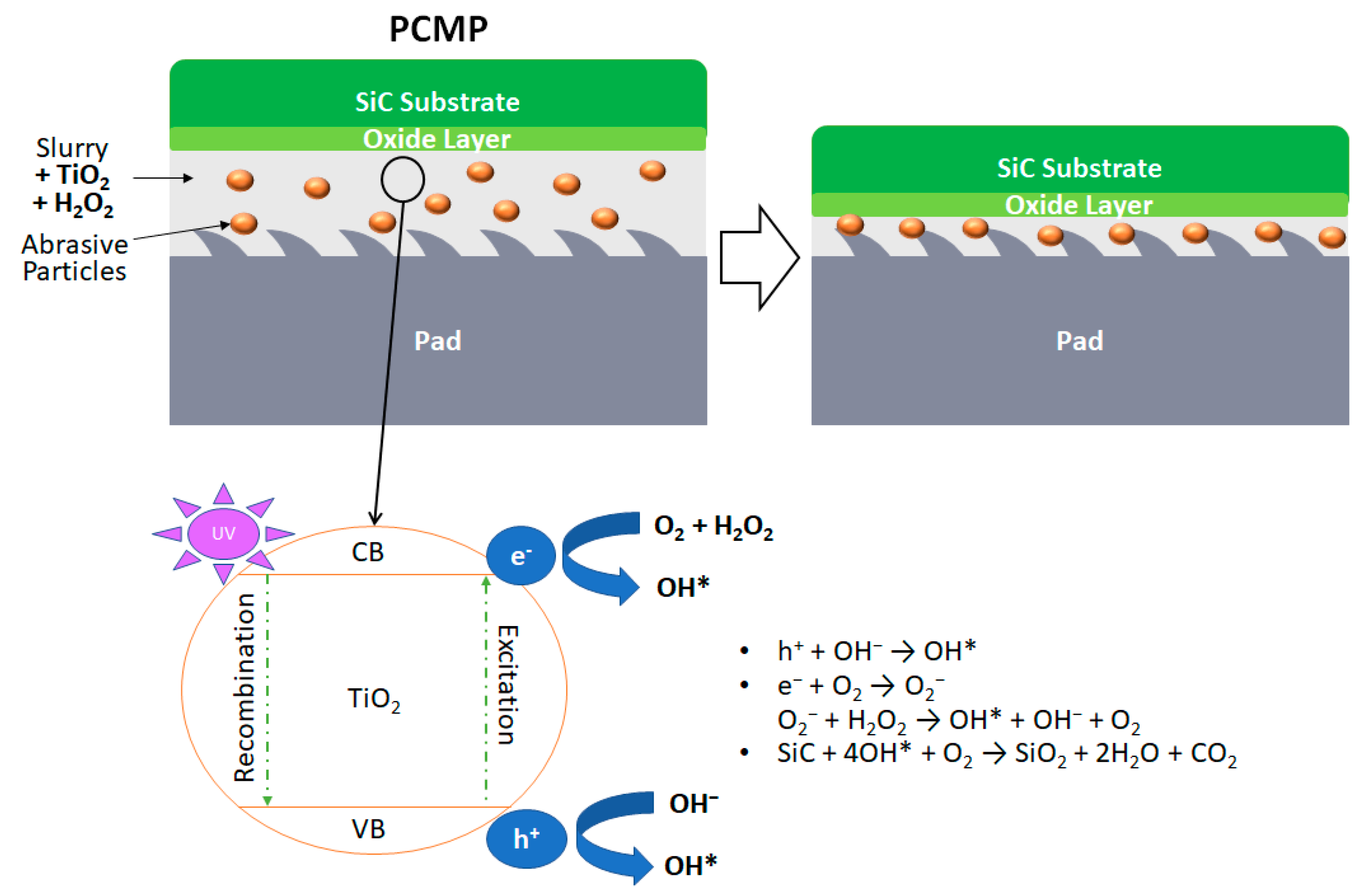
2.3. SiC Photocatalyzed-CMP (PCMP)

Photocatalyzed-CMP (PCMP) adds an additional oxidation source by applying UV light to highly photocatalytic particles, such as TiO2. The hydroxyl radicals generated by the photocatalytic process enhance the oxidation efficiency as well as the MRR (Figure 6 and Figure 7). In 2018, Yuan et al. proposed that photocatalysts, UV light, electron capturers and an acidic environment are the key factors in PCMP [31]. The MRR and surface roughness (Ra) equal to 0.96 µm h−1 and 1.95 nm, respectively, on the 4H-SiC surface, can be obtained by using synthetic fibrous polymer pads and applying UV light on the slurry consisting of TiO2 and H2O2 at pH = 2, polishing pressure = 0.025 MPa and rotation speed = 60 rpm. Compared to the control groups using TiO2 + H2O2 + pH 2 and TiO2 + UV + pH 2, the experimental group using TiO2 + UV + H2O2 + pH 2 yields the best polishing result [31]. In 2021, Wang et al. introduced a sulfate radical-based advanced oxidation process which applies sulfate (K2S2O8) into the PCMP system (sulfate-PCMP) [32]. Similar to the functionality of H2O2, the sulfate tends to generate SO4 radicals during the PCMP process. Under the conditions of 3 wt% sulfate, 0.02 wt% TiO2 and pH 6 in the slurry, the highest MRR can be obtained [32].
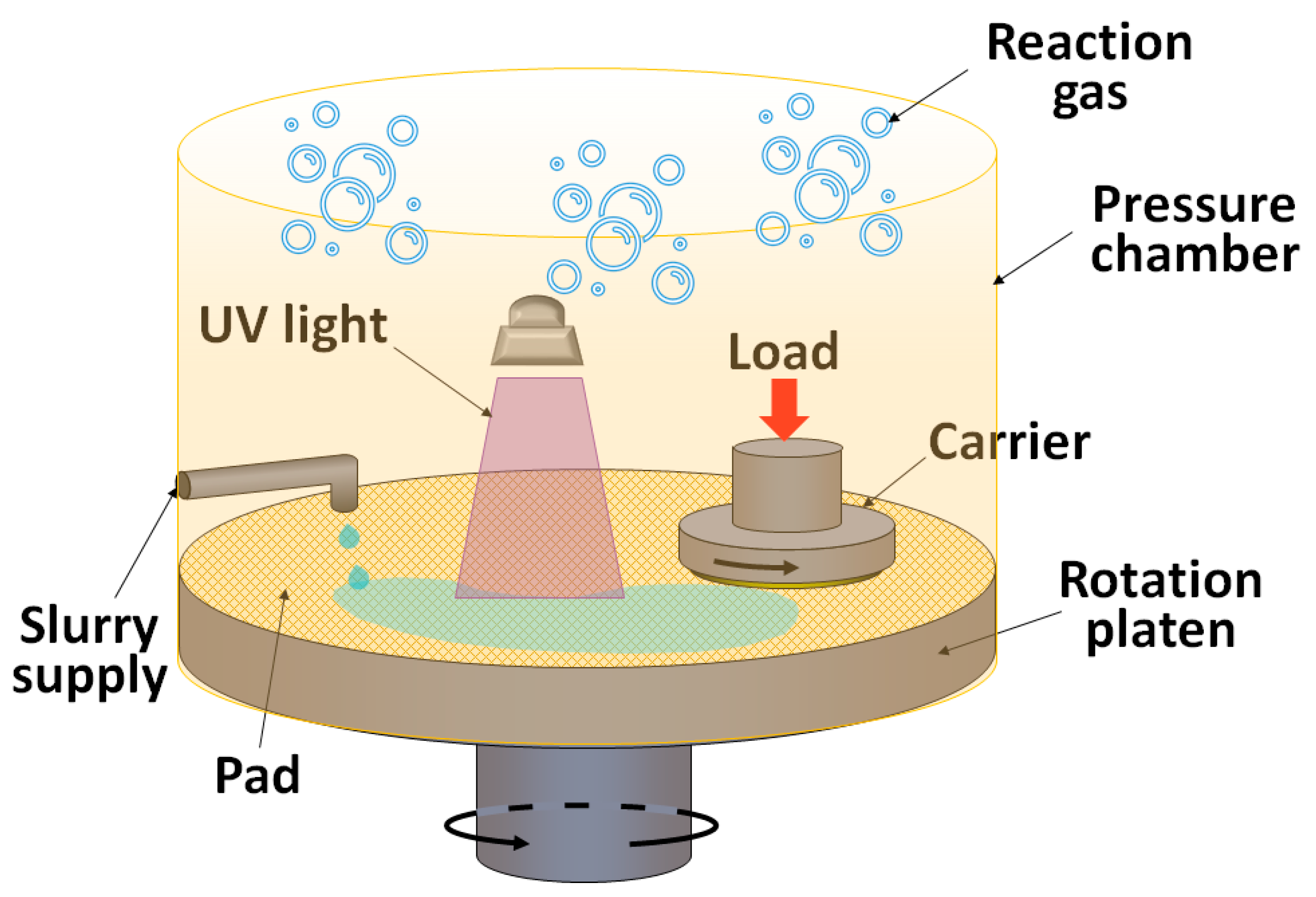
In 2021, Yin et al. developed a new PCMP method, in which the PCMP was conducted in an enclosed chamber filled with different compositions of gases, such as air, O2 and N2 (gas-PCMP, Figure 8) [34]. The highest MRR and dissolved oxygen (DO) amount were obtained on both Si-face surface (MRR = 43 nm h−1 and DO = 57 mg L−1) and C-face surface (MRR =108 nm h−1 and DO = 57 mg L−1) with the oxygen partial pressure equal to 300 kPa. By adding 0.3 wt% TiO2 particles and UV illumination into the system, the MRR can be increased by 30% and 10% on the Si-face and C-face surfaces, respectively. The MRR on the Si-face surface was about 2.2-fold higher than open air CMP [34]. In 2021, Lu et al. proposed a UV-photocatalyzed-Fenton combined mechanism for CMP, aiming at increasing the hydroxyl concentration as well as the MRR (Fenton-PCMP) [35]. Under the conditions of polishing pressure = 0.04 MPa, rotation speed = 60 rpm, slurry flow rate = 33 mL min−1 and using a polyurethane pad, the highest MRR of 387.2 nm h−1 on the C-face surface was obtained from the UV + TiO2 (4 g L−1) + Fenton group. The phenomenon that UV illumination could lead to better surface roughness was observed not only for the UV + TiO2 (4 g L−1) + H2O2 (5 wt%) group and UV + TiO2 (4 g L−1) + Fenton group, but also for the UV + H2O2 (5 wt%) group and UV + Fenton group. Moreover, the MRR holds a negative relationship with the surface roughness in the UV-illuminated groups [35].

3. Post-SiC CMP Cleaning

As described in Table 1, the main purpose of the SiC post-CMP cleaning is to remove organic, metallic and abrasive contaminations resulting from the CMP process, so as to achieve high-quality epitaxial growth in the following step [36]. Owing to the chemical inertness of SiC, traditional post-CMP cleaning methods, such as RCA and sulfuric peroxide mix (SPM), whose working principles are based on oxidation followed by etching, become problematic. In 2008, Madani et al. proposed an idea to remove the foreign bodies by directly reacting with them instead of micro-etching the substrate [37]. Hydrogen cyanide (HCN) solution was used in the study, which can provide cyanide ions to react with the metal contaminants. After the 4H-SiC wafer was immersed in the 0.08 M CuCl2 and 0.08 M NiCl2 solution for 10 min, the wafer was sequentially cleaned by the APM (29 wt% NH4OH:30 wt% H2O2:H2O = 1:1:5), HPM (36 wt% HCl:30 wt% H2O2:H2O = 1:1:5) and HCN solutions. Based on the total reflection X-ray fluorescence (TXRF) results, the Cu and Ni ions were completely removed by cleaning with 80 °C HPM followed by 25 °C HCN [37].
Although metal ions can be removed by HCN, how to remove other kinds of foreign bodies simultaneously raises the complexity of cleaning agent design, as well as the concerns for integrating into current manufacturing facilities. In 2022, Cahue et al. developed a contact cleaning method involving a poly-vinyl alcohol (PVA) brush, which transfers cleaning chemistry to the substrate and provides a mechanical force for efficient contamination removal [38]. After immersing the 4H-SiC wafer in a pH 4 slurry containing 0.005 wt% Al2O3 abrasive particles, the cleaning efficiencies with a brush only and after the addition of encapsulating chemicals were investigated. The particle count of the incoming dried wafer was around 10,000 ea and decreased to 6000 ea with a brush and deionized water. When both brush and encapsulating chemicals were applied, the particle count significantly decreased to 2000 ea. A similar trend was observed when the PVA brush was replaced with a megasonic mechanical source (30 sec and 1.5 W cm−2) [38].

4. Conclusions and Prospects

In this review article, we discuss the production steps from the SiC boule to epitaxy-ready substrates. Three configurations of SiC CMP currently used in the industry and their advantages/disadvantages are compared. The mechanisms that cause different surface properties as well as oxidation behaviors on the Si-face and C-face surfaces are discussed. Hybrid CMP technologies, such as ECMP, Fenton-ECMP, ultrasonic-ECMP, PCMP, sulfate-PCMP, gas-PCMP and Fenton-PCMP, give rise to the potential of increasing MRR while decreasing surface roughness. The operation conditions and performance parameters of various CMP technologies discussed in this article are summarized in Table 3. Lastly, the importance of post-CMP cleaning to the following epitaxial growth is pointed out. Cleaning with heated HPM and HCN solutions sequentially or applying a PVA brush has been proven to be able to remove metal ions and abrasive particles effectively. Upon the foundation of this review article, the research topics worth further investigation are suggested as follows. (1) How to utilize the unique structures of synthetic abrasive particles to enhance the CMP or hybrid CMP performance. (2) The trend of integrating multiple forms of energy into CMP has been obvious. However, how the interactions among these energy forms lead to the improvement of MRR and surface roughness is still not quite clear and needs further investigation.

Author Contributions

Data collection and original draft preparation, C.-H.H. and C.-Y.C.; review and editing, C.-C.T.; supervision, Y.-K.H., C.-C.A.C., C.-C.T. and H.-C.K. All authors have read and agreed to the published version of the manuscript.

Funding

This research received no external funding.

Data Availability Statement

Not applicable.

Acknowledgments

This work is financially supported by the Hon Hai Research Institute, Foxconn Technology Group. The authors also like express their sincere gratitude to Taisic Materials Corp. for their consistent technical support.

Conflicts of Interest

The authors declare no conflict of interest.

References

  1. Langpoklakpam, C.; Liu, A.-C.; Chu, K.-H.; Hsu, L.-H.; Lee, W.-C.; Chen, S.-C.; Sun, C.-W.; Shih, M.-H.; Lee, K.-Y.; Kuo, H.-C. Review of Silicon Carbide Processing for Power MOSFET. Crystals 2022, 12, 245. [Google Scholar] [CrossRef]
  2. Yu, S.; Hu, J.J.; Xu, L.L.; Liu, M.; Liu, E.; Givens, J.; Leighton, J. Highest Quality and Repeatability for Single Wafer 150 mm SiC CMP Designed for High Volume Manufacturing. Mater. Sci. Forum 2022, 1062, 229–234. [Google Scholar] [CrossRef]
  3. Song, C.; Shi, F.; Zhang, W.; Lin, Z.; Lin, Y. High-Efficiency and Low-Damage Lapping Process Optimization. Materials 2020, 13, 569. [Google Scholar] [CrossRef] [Green Version]
  4. Ji, P.; Zhang, K.; Zhang, Z.; Zhao, M.; Li, R.; Hao, D.; Moro, R.; Ma, Y.; Ma, L. A General Strategy for Polishing SiC Wafers to Atomic Smoothness with Arbitrary Facets. Mater. Sci. Semicond. Process. 2022, 144, 106628. [Google Scholar] [CrossRef]
  5. Lu, J.; Luo, Q.; Xu, X.; Huang, H.; Jiang, F. Removal Mechanism of 4H- and 6H-SiC Substrates (0001 and 0001) in Mechanical Planarization Machining. Proc. Inst. Mech. Eng. B 2019, 233, 69–76. [Google Scholar] [CrossRef]
  6. Shi, S.; Yu, Y.; Wang, N.; Zhang, Y.; Shi, W.; Liao, X.; Duan, N. Investigation of the Anisotropy of 4H-SiC Materials in Nanoindentation and Scratch Experiments. Materials 2022, 15, 2496. [Google Scholar] [CrossRef] [PubMed]
  7. Nitta, H.; Isobe, A.; Hong, P.J.; Hirao, T. Research on Reaction Method of High Removal Rate Chemical Mechanical Polishing Slurry for 4H-SiC Substrate. Jpn. J. Appl. Phys. 2011, 50, 046501. [Google Scholar] [CrossRef]
  8. Pan, G.; Zhou, Y.; Luo, G.; Shi, X.; Zou, C.; Gong, H. Chemical Mechanical Polishing (CMP) of On-Axis Si-Face 6H-SiC Wafer for Obtaining Atomically Flat Defect-Free Surface. J. Mater. Sci. Mater. Electron. 2013, 24, 5040–5047. [Google Scholar] [CrossRef]
  9. Chen, G.; Ni, Z.; Bai, Y.; Li, Q.; Zhao, Y. The Role of Interactions between Abrasive Particles and the Substrate Surface in Chemical-Mechanical Planarization of Si-Face 6H-SiC. RSC Adv. 2017, 7, 16938–16952. [Google Scholar] [CrossRef] [Green Version]
  10. Tsai, Y.; Chen, C.; Suzuki, K.; Khajornrungruang, P.; Chiu, S.; Hua, C. Advanced Chemical–Mechanical Planarization for 4H-SiC Substrate by Water-Soluble Inclusion Complexes of Fullerene. Jpn. J. Appl. Phys. 2020, 59, SLLA01. [Google Scholar] [CrossRef]
  11. Qi, W.; Cao, X.; Xiao, W.; Wang, Z.; Su, J. Study on the Mechanism of Solid-Phase Oxidant Action in Tribochemical Mechanical Polishing of SiC Single Crystal Substrate. Micromachines 2021, 12, 1547. [Google Scholar] [CrossRef] [PubMed]
  12. Ni, Z.; Chen, G.; Xu, L.; Zhang, P.; Dai, M.; Qian, S.; Bian, D.; Zhang, H. Preparation of Ceria-Coated Silica Nanoparticles and Their Chemical Mechanical Planarization Performance on Si-Face 6H-SiC Substrates. J. Solid State Sci. Technol. 2021, 10, 123011. [Google Scholar] [CrossRef]
  13. Singh, B.P.; Jena, J.; Besra, L.; Bhattacharjee, S. Dispersion of Nano-Silicon Carbide (SiC) Powder in Aqueous Suspensions. J. Nanoparticle Res. 2007, 9, 797–806. [Google Scholar] [CrossRef]
  14. Chen, G.; Ni, Z.; Xu, L.; Li, Q.; Zhao, Y. Performance of Colloidal Silica and Ceria Based Slurries on CMP of Si-Face 6H-SiC Substrates. Appl. Surf. Sci. 2015, 359, 664–668. [Google Scholar] [CrossRef]
  15. Wang, W.; Liu, W.; Song, Z. Two-Step Chemical Mechanical Polishing of 4H-SiC (0001) Wafer. ECS J. Solid State Sci. Technol. 2021, 10, 074004. [Google Scholar] [CrossRef]
  16. Wang, W.; Zhang, B.; Shi, Y.; Zhou, D.; Wang, R. Improvement in Dispersion Stability of Alumina Suspensions and Corresponding Chemical Mechanical Polishing Performance. Appl. Surf. Sci. 2022, 597, 153703. [Google Scholar] [CrossRef]
  17. Wang, H.; Niu, F.; Chen, J.; Jiang, Z.; Wang, W.; Bu, Z.; Wang, X.; Li, J.; Zhu, Y.; Sun, T. High Efficiency Polishing of Silicon Carbide by Applying Reactive Non-Aqueous Fluids to Fixed Abrasive Pads. Ceram. Int. 2022, 48, 7273–7282. [Google Scholar] [CrossRef]
  18. Zhou, P.; Zhu, N.; Xu, C.; Niu, F.; Li, J.; Zhu, Y. Mechanical Removal of SiC by Multi-Abrasive Particles in Fixed Abrasive Polishing Using Molecular Dynamics Simulation. Comput. Mater. Sci. 2021, 191, 110311. [Google Scholar] [CrossRef]
  19. Lu, J.; Li, Y.; Xu, X. The Effects of Abrasive Yielding on the Polishing of SiC Wafers Using a Semi-Fixed Flexible Pad. Proc. Inst. Mech. Eng. B J. Eng. Manuf. 2015, 229, 170–177. [Google Scholar] [CrossRef]
  20. Luo, Q.; Wen, H.; Lu, J. Sol–Gel Polishing Technology for Extremely Hard Semiconductor Substrates. Int. J. Adv. Manuf. Technol. 2022, 120, 1415–1432. [Google Scholar] [CrossRef]
  21. Kayanuma, M.; Kato, T.; Morishita, T. Reaction Mechanisms of the Initial Steps for the Oxidation of (0001) C and (0001) Si Faces of SiC with OH Radicals. Surf. Sci. 2022, 719, 122031. [Google Scholar] [CrossRef]
  22. Morishita, T.; Kayanuma, M.; Nakamura, T.; Kato, T. Cooperative Reaction of Hydrogen-Networked Water Molecules at the SiC–H2O2 Solution Interface: Microscopic Insights from Ab Initio Molecular Dynamics. J. Phys. Chem. C 2022, 126, 12441–12449. [Google Scholar] [CrossRef]
  23. Ma, G.; Li, S.; Liu, F.; Zhang, C.; Jia, Z.; Yin, X. A Review on Precision Polishing Technology of Single-Crystal SiC. Crystals 2022, 12, 101. [Google Scholar] [CrossRef]
  24. Chen, C.-C.A.; Hsieh, C.-H. Effect of Inhibiter Concentration on Cu CMP Slurry Analyzed by a Cu-ECMP System. ECS Trans. 2010, 33, 107–113. [Google Scholar] [CrossRef]
  25. Chen, Z.; Zhao, Y. Investigation into Electrochemical Oxidation Behavior of 4H-SiC with Varying Anodizing Conditions. Electrochem. Commun. 2019, 109, 106608. [Google Scholar] [CrossRef]
  26. Deng, H.; Hosoya, K.; Imanishi, Y.; Endo, K.; Yamamura, K. Electro-Chemical Mechanical Polishing of Single-Crystal SiC Using CeO2 Slurry. Electrochem. Commun. 2015, 52, 5–8. [Google Scholar] [CrossRef] [Green Version]
  27. Deng, J.; Pan, J.; Zhang, Q.; Yan, Q.; Lu, J. The Mechanism of Fenton Reaction of Hydrogen Peroxide with Single Crystal 6H-SiC Substrate. Surf. Interfaces 2020, 21, 100730. [Google Scholar] [CrossRef]
  28. Deng, J.; Lu, J.; Yan, Q.; Pan, J. Enhancement Mechanism of Chemical Mechanical Polishing for Single-Crystal 6H-SiC Based on Electro-Fenton Reaction. Diam. Relat. Mater. 2021, 111, 108147. [Google Scholar] [CrossRef]
  29. Yang, X.; Yang, X.; Kawai, K.; Arima, K.; Yamamura, K. Novel SiC Wafer Manufacturing Process Employing Three-Step Slurryless Electrochemical Mechanical Polishing. J. Manuf. Process. 2021, 70, 350–360. [Google Scholar] [CrossRef]
  30. Yang, X.; Yang, X.; Gu, H.; Kawai, K.; Arima, K.; Yamamura, K. Efficient and Slurryless Ultrasonic Vibration Assisted Electrochemical Mechanical Polishing for 4H-SiC Wafers. Ceram. Int. 2022, 48, 7570–7583. [Google Scholar] [CrossRef]
  31. Yuan, Z.; He, Y.; Sun, X.; Wen, Q. UV-TiO2 Photocatalysis-Assisted Chemical Mechanical Polishing 4H-SiC Wafer. Mater. Manuf. 2018, 33, 1214–1222. [Google Scholar] [CrossRef]
  32. Wang, W.; Zhang, B.; Shi, Y.; Ma, T.; Zhou, J.; Wang, R.; Wang, H.; Zeng, N. Improvement in Chemical Mechanical Polishing of 4H-SiC Wafer by Activating Persulfate through the Synergistic Effect of UV and TiO2. J. Mater. Process. Technol. 2021, 295, 117150. [Google Scholar] [CrossRef]
  33. Zhou, Y.; Pan, G.; Zou, C.; Wang, L. Chemical Mechanical Polishing (CMP) of SiC Wafer Using Photo-Catalyst Incorporated Pad. ECS J. Solid State Sci. Technol. 2017, 6, 603. [Google Scholar] [CrossRef]
  34. Yin, T.; Zhao, P.; Doi, T.; Kurokawa, S.; Jiang, J. Effect of Using High-Pressure Gas Atmosphere with UV Photocatalysis on the CMP Characteristics of a 4H-SiC Substrate. ECS J. Solid State Sci. Technol. 2021, 10, 024010. [Google Scholar] [CrossRef]
  35. Lu, J.; Huang, Y.; Fu, Y.; Yan, Q.; Zeng, S. Synergistic Effect of Photocatalysis and Fenton on Improving the Removal Rate of 4H-SiC during CMP. ECS J. Solid State Sci. Technol. 2021, 10, 024010. [Google Scholar] [CrossRef]
  36. Chen, P.-C.; Miao, W.-C.; Ahmed, T.; Pan, Y.-Y.; Lin, C.-L.; Chen, S.-C.; Kuo, H.-C.; Tsui, B.-Y.; Lien, D.-H. Defect Inspection Techniques in SiC. Nanoscale Res. Lett. 2022, 17, 30. [Google Scholar] [CrossRef]
  37. Madani, M.; Liu, Y.-L.; Takahashi, M.; Iwasa, H.; Kobayashi, H. SiC Cleaning Method by Use of Dilute HCN Aqueous Solutions. J. Electrochem. Soc. 2008, 155, H895. [Google Scholar] [CrossRef]
  38. Cahue, K.A.; Dudek, A.L.; Miliauskas, M.M.; Cahue, T.R.; Mlynarski, A.; Keleher, J.J. Design of “Low Stress” Post-CMP Cleaning Processes for Advanced Technology Nodes. ECS Trans. 2022, 108, 3. [Google Scholar] [CrossRef]
Figure 1. Illustrations of surface roughness and subsurface damage depth at the slicing, lapping, grinding and CMP steps of the SiC wafer production process [3].
Micromachines 13 01752 g001
Figure 2. Different configurations of SiC CMP, including (A) batch wafer and single-sided CMP, (B) batch water and double-sided CMP and (C) single wafer and single-sided CMP. (Ref. CMC Materials Co.).
Micromachines 13 01752 g002
Figure 3. (A) Illustration of CMP mechanism. The oxidants in the slurry oxidize the SiC surface into a softer oxide layer which can be removed by the abrasive particles in the slurry and the conditioned CMP pad simultaneously. The chemical reactions of SiC oxidation, which are initiated by either oxygens or hydroxyl radicals, are shown [7,8]. Note that asterisk represents radicals. (B) Illustration of Tribo-CMP mechanism. In addition to the global oxidation taking place at the slurry and SiC interface, localized oxidation can also occur when the solid-phase abrasive oxidants roll on the SiC wafer surface.
Micromachines 13 01752 g003
Figure 4. Typical setup for SiC ECMP.
Micromachines 13 01752 g004
Figure 5. (A) Illustration of Fenton-ECMP mechanism. The oxidants and Fe3O4 catalyst in the slurry oxidize the SiC surface into a softer oxide layer which can be removed by the abrasive particles in the slurry and the conditioned CMP pad simultaneously. Under acidic conditions, Fe3O4 generates Fe2+ which undergoes a Fenton reaction with H2O2 to generate strong oxidant hydroxyl radical, denoted as OH* [27]. The oxide layer is removed by the abrasive particles in the slurry and the conditioned CMP pad simultaneously. (B) Illustration of ultrasonic-ECMP mechanism. After the anodic oxidation of SiC, the oxide layer is removed by a vibrating grinding stone with fixed abrasives.
Micromachines 13 01752 g005
Figure 6. Typical setup for SiC PCMP.
Micromachines 13 01752 g006
Figure 7. Illustration of PCMP mechanism. Upon irradiation of UV light, the photocatalytic TiO2 particle reacts with O2, H2O and OH in the slurry to generate strong oxidant hydroxyl radical, denoted as OH* [33]. The oxide layer is then removed by the abrasive particles in the slurry and the conditioned CMP pad simultaneously.
Micromachines 13 01752 g007
Figure 8. Typical setup for SiC gas-PCMP.
Micromachines 13 01752 g008
Table 1. SiC wafer production steps and the purposes. (Ref. CMC Materials Co., Kaohsiung City, Taiwan).
Production StepPurpose
Cropping/Blocking
  • To cut off the boule’s head and tail, creating a flat datum plane.
  • To shape the boule’s body into the desired diameter.
Creating Flat/Notch
  • To create alignment of the ingot.
Slicing
  • To cut the ingot into wafers with the desired thickness.
Edge Grinding
  • To create a shaped edge, for reducing edge chipping risk and increasing epitaxial film uniformity.
Laser Marking
  • To create an identification number of each wafer.
Lapping
  • To make the wafer thickness uniform.
  • To lower the total thickness variation resulting from the slicing step.
Grinding
  • To lower the surface roughness level to nanometer scale.
  • To minimize subsurface damage depth by using diamond grinding wheel.
CMP
  • To lower the surface roughness level to angstrom scale.
  • To remove grinding marks, scratches and subsurface damages.
Post-CMP Cleaning
  • To remove abrasives and other organic and metallic contaminations from the wafer surface.
Inspecting
  • To ensure the wafer surface qualities, such as scratch, haze and metal levels, particle count and topology, meet the required specifications.
Packaging
  • To prepare the wafer ready for the subsequent epitaxial application.
Table 2. Comparison between different configurations of SiC CMP. (Ref. CMC Materials Co.).
Single/Batch WaferSingle/Double Sided CMPAdvantagesDisadvantages
BatchSingle
  • Widely used in the mass production of 100-mm and 150-mm SiC wafers.
  • Total thickness variation increases with CMP time.
  • Same defects tend to appear on other wafers within the same batch.
BatchDouble
  • Low total thickness variation
  • Lowest MRR
  • Different removal rates on Si-face and C-face surfaces
SingleSingle
  • Suitable for the mass production of 200-mm SiC wafers
  • Flexible local flatness control by multi-pressure zone method
  • Highest MRR
  • Membrane assisted wafer holding saves loading and unloading times
  • Highest initial capital investment
Table 3. Operation conditions and performance parameters, namely MRR and surface roughness, of the various CMP and hybrid CMP technologies discussed in this article.
Energy TypeMRR (µm h−1)Surface Roughness (nm)NoteRef.
CMP
  • Chemical
  • Mechanical
  • Si-face: 6.4
  • C-face: 22.5
  • Si-face: 0.1 (Ra)
  • C-face: 0.4 (Ra)
  • 4H-SiC
  • Pressure (psi) × rotation speed (rpm)/100 = 9
  • Al2O3 abrasive
  • Polyurethane pad
[2]
ECMP
  • Electrical
  • Chemical
  • Mechanical
  • Si-face: 0.42
  • C-face: 3.62
  • Si-face: 0.23 (RMS)
  • 4H-SiC
  • Applied voltage = 10 V
  • Pressure (psi) × rotation speed (rpm)/100 = 10.8
  • CeO2 abrasive for Si-face
  • Diamond abrasive for C-face
  • PET pad
[26]
Fenton-ECMP
  • Electrical
  • Chemical (Fenton)
  • Mechanical
  • C-face: 0.443
  • C-face: 31.1 (Ra)
  • 6H-SiC
  • Applied voltage = 3 V
  • Pressure (psi) × rotation speed (rpm)/100 = 3
  • SiO2 abrasive
  • Polyurethane pad
[28]
Ultrasonic-ECMP
  • Electrical
  • Chemical
  • Mechanical (ultrasound)
  • 14.54
  • 1.993 (Sq)
  • 4H-SiC
  • Applied voltage = 25 V
  • Vibrator: 500 W and 35 kHz
  • Pressure (psi) × rotation speed (rpm)/100 = 8.7
  • Fixed abrasive pad
[30]
PCMP
  • Chemical
  • Mechanical
  • UV
  • 0.96
  • 1.95 (Ra)
  • 4H-SiC
  • Pressure (psi) × rotation speed (rpm)/100 = 3.6
  • Fibrous polymer pad
[31]
Gas-PCMP
  • Chemical
  • Mechanical
  • UV
  • Si-face: 0.07
  • Si-face: 0.98 (Ra)
  • 4H-SiC
  • O2 (300 kPa) + SiO2 abrasive + TiO2 photocatalyst
  • Pressure (psi) × rotation speed (rpm)/100 = 2.4
  • Polyurethane pad
[34]
Fenton-PCMP
  • Chemical (Fenton)
  • Mechanical
  • UV
  • C-face: 0.387
  • C-face: 5.07 (Ra)
  • 4H-SiC
  • Pressure (psi) × rotation speed (rpm)/100 = 3.48
  • Polyurethane pad
[35]
Publisher’s Note: MDPI stays neutral with regard to jurisdictional claims in published maps and institutional affiliations.

