
A Study on Over-Molded Copper-Based Flexible Electronic Circuits

Abstract
:1. Introduction
2. Experimental Procedures
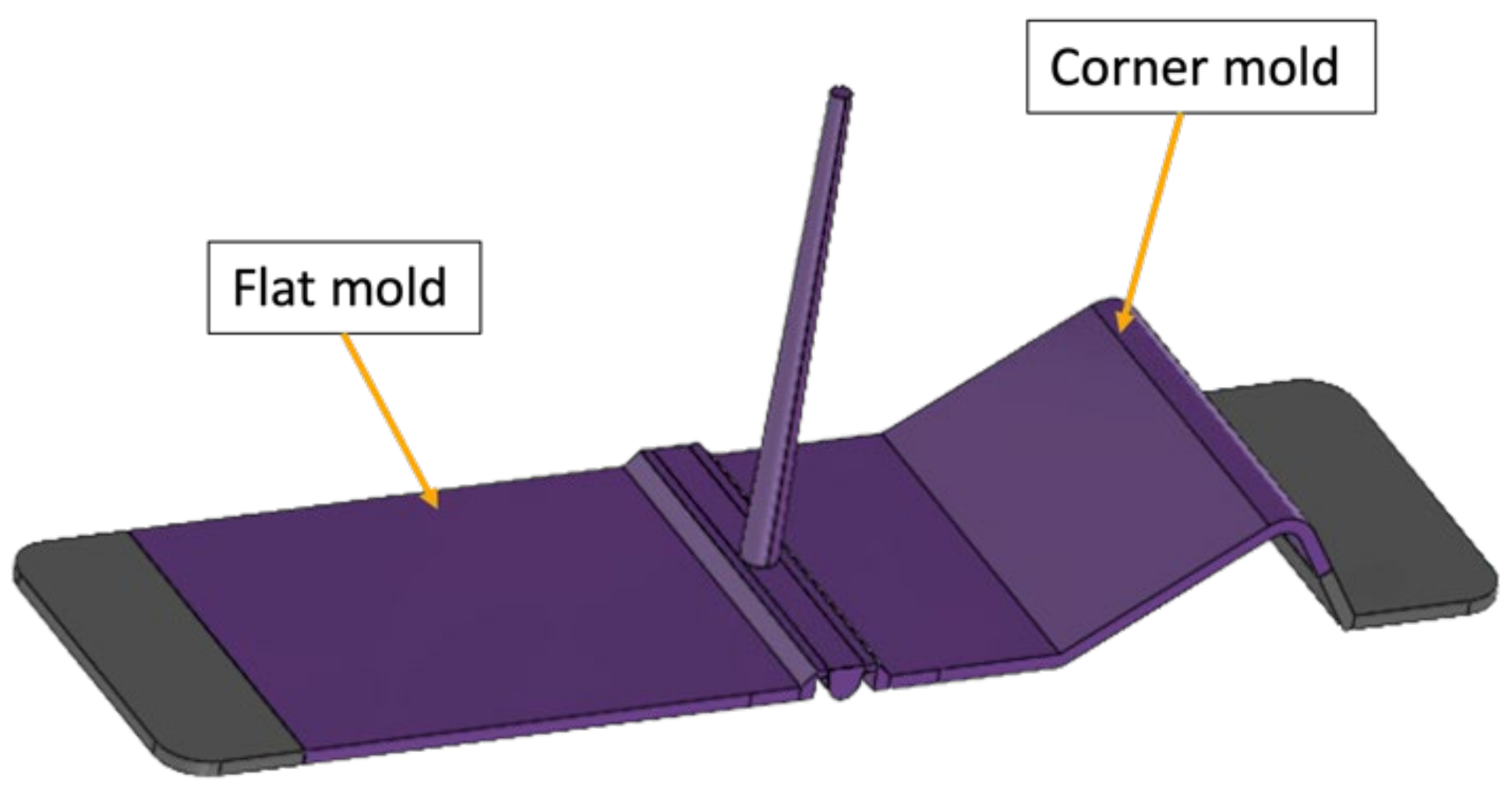
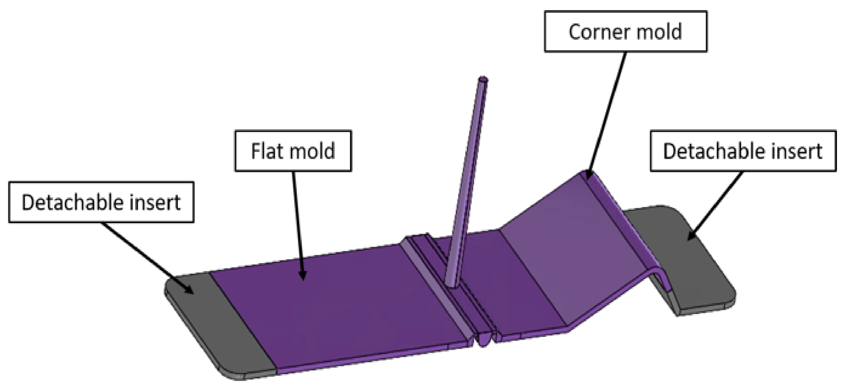
2.1. Mold Design
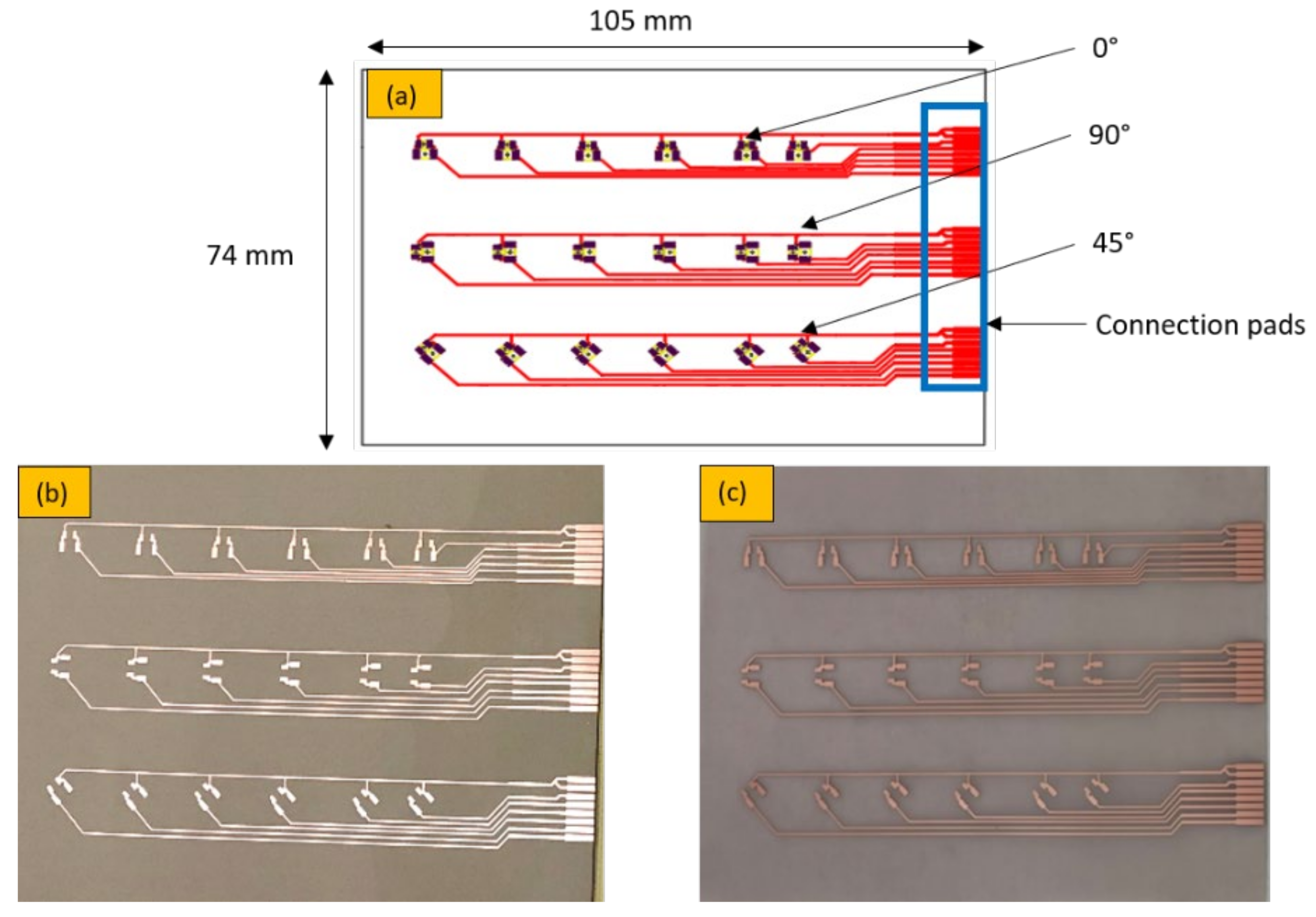
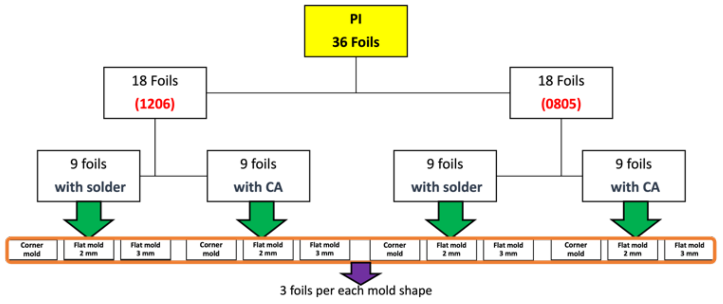
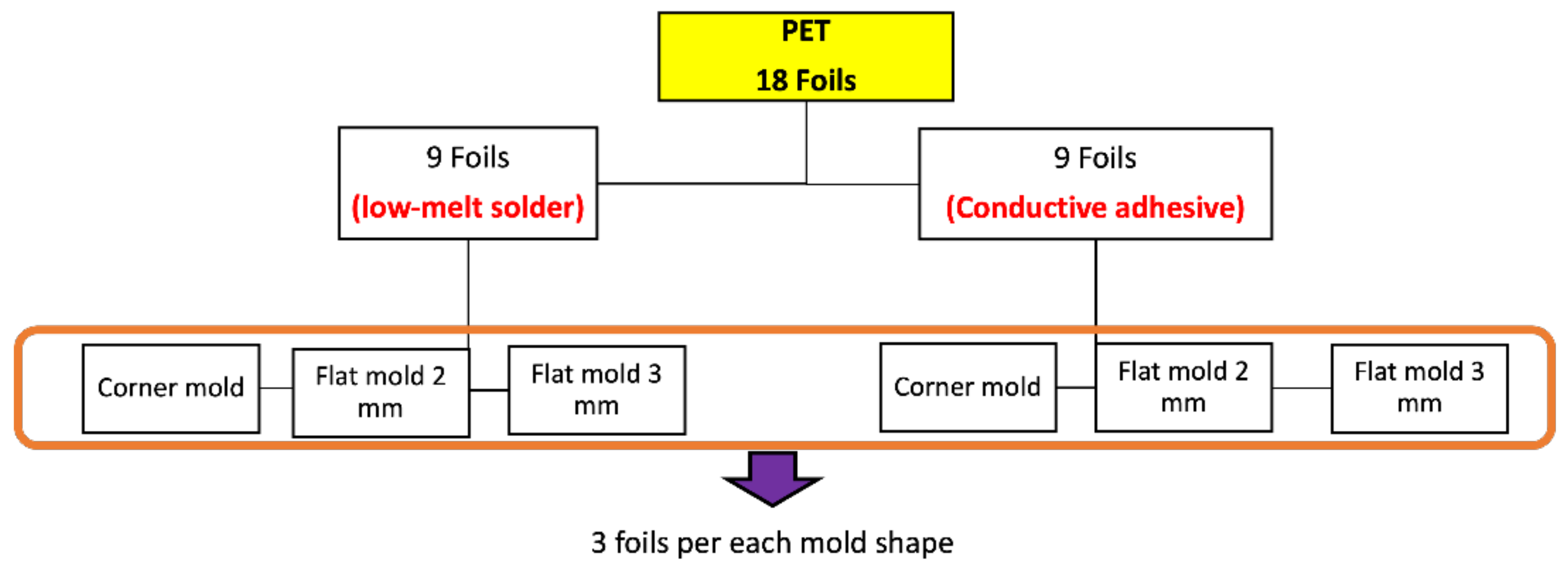
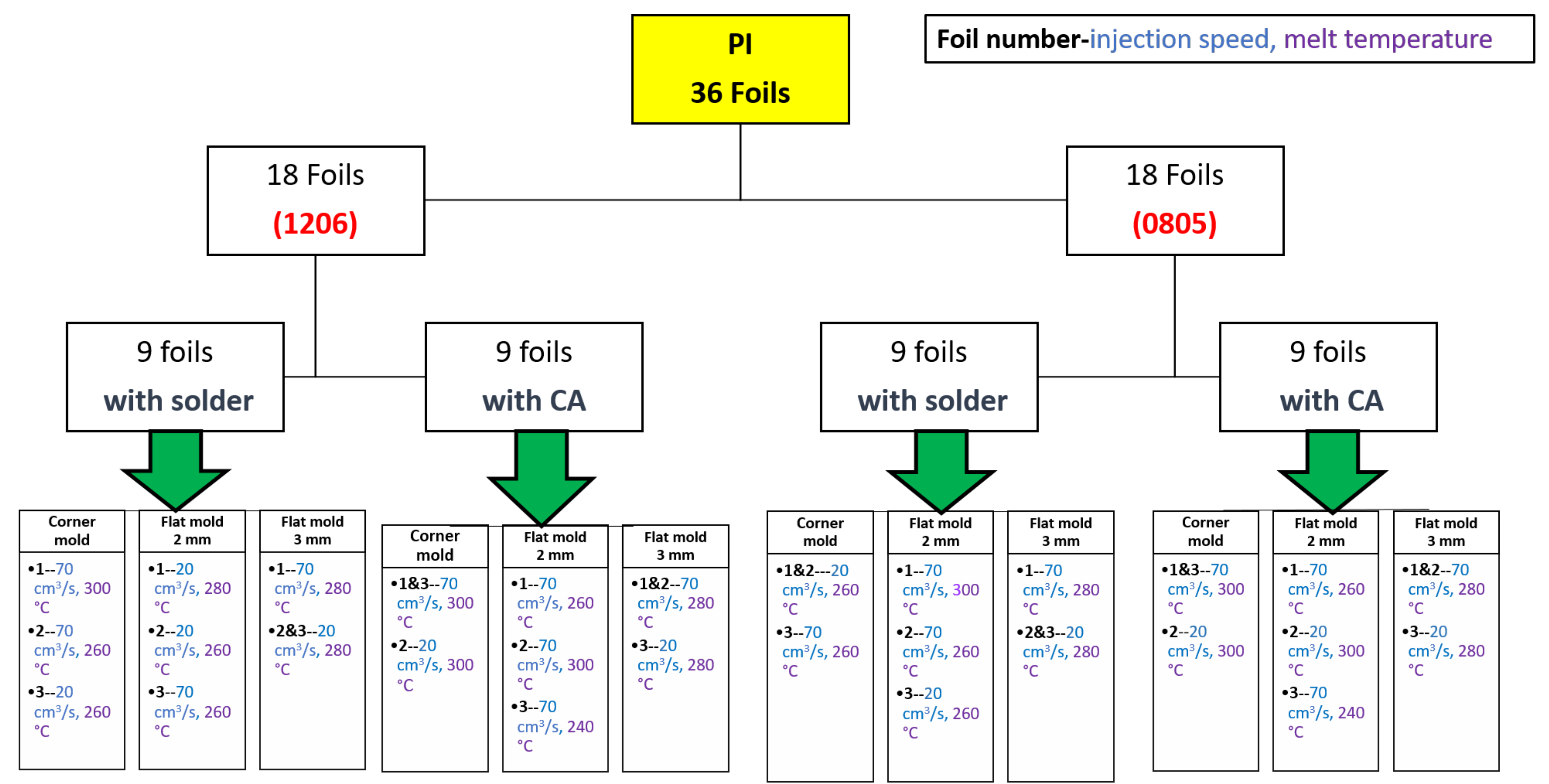
2.2. Foil Design
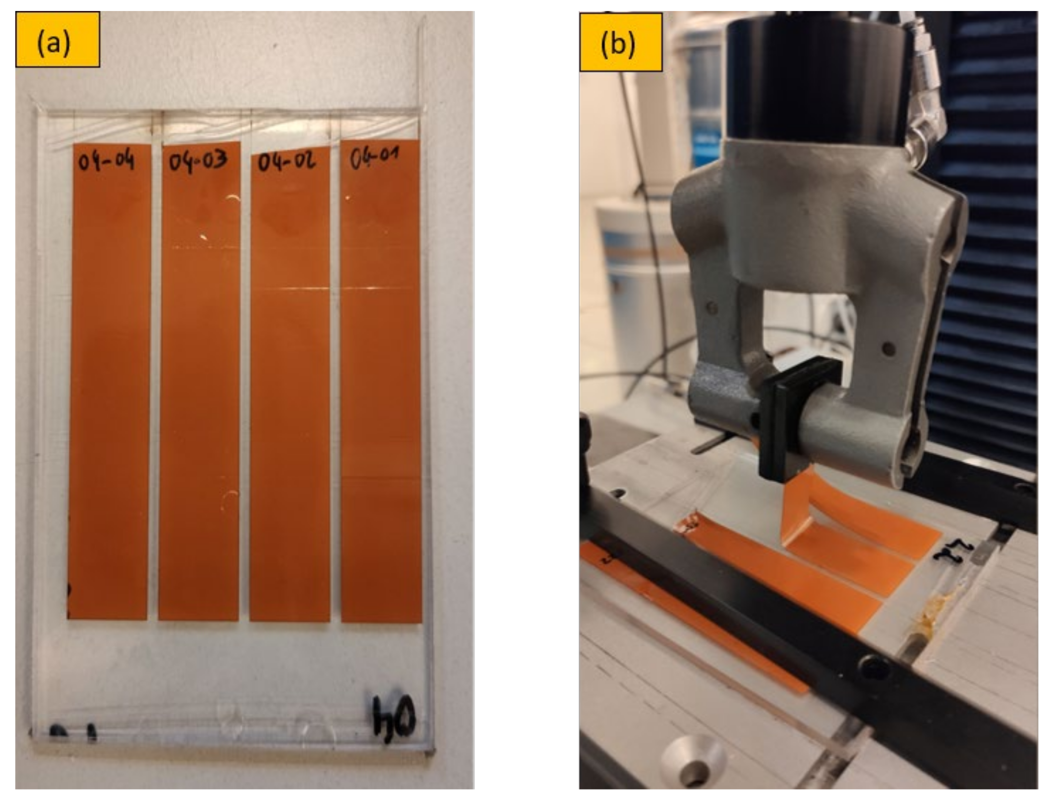
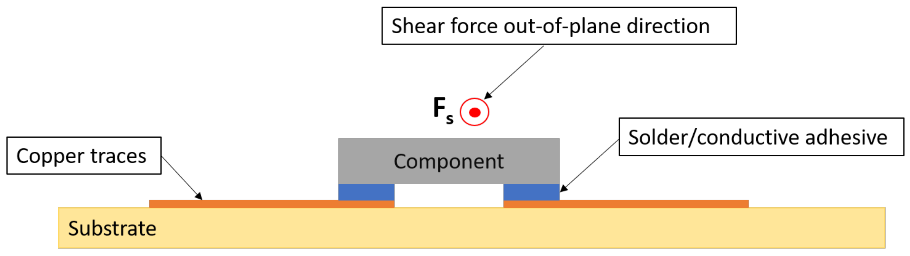
2.3. Adhesion and Peel Tests
2.4. Simulation
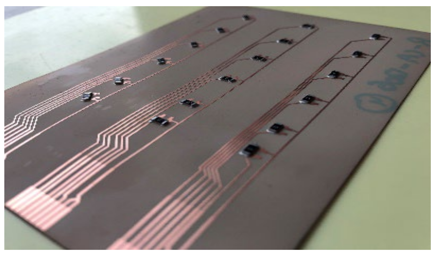
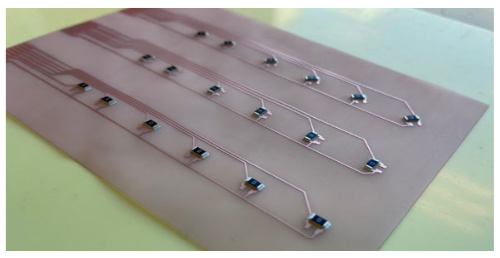
2.5. Foil Fabrication and Assembly
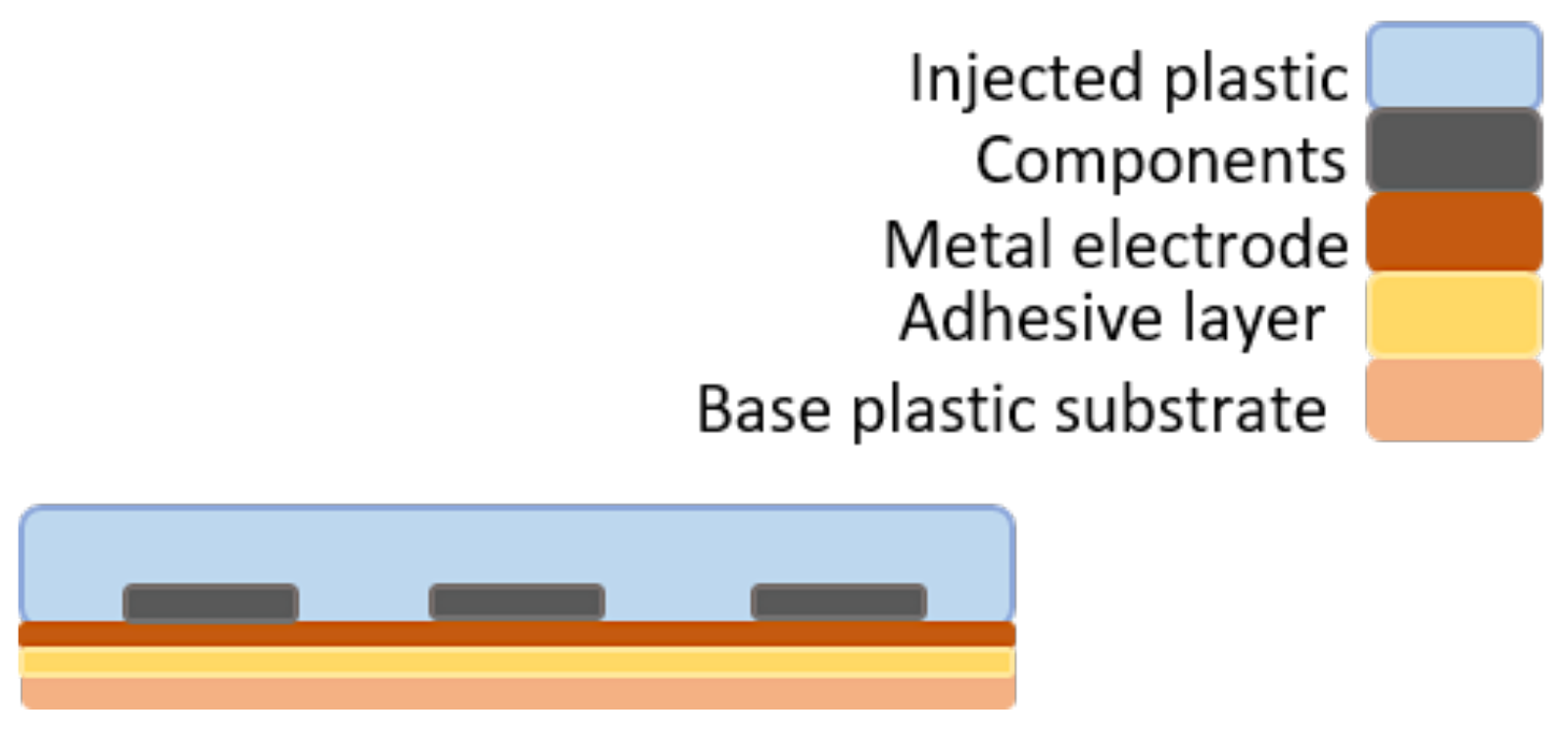
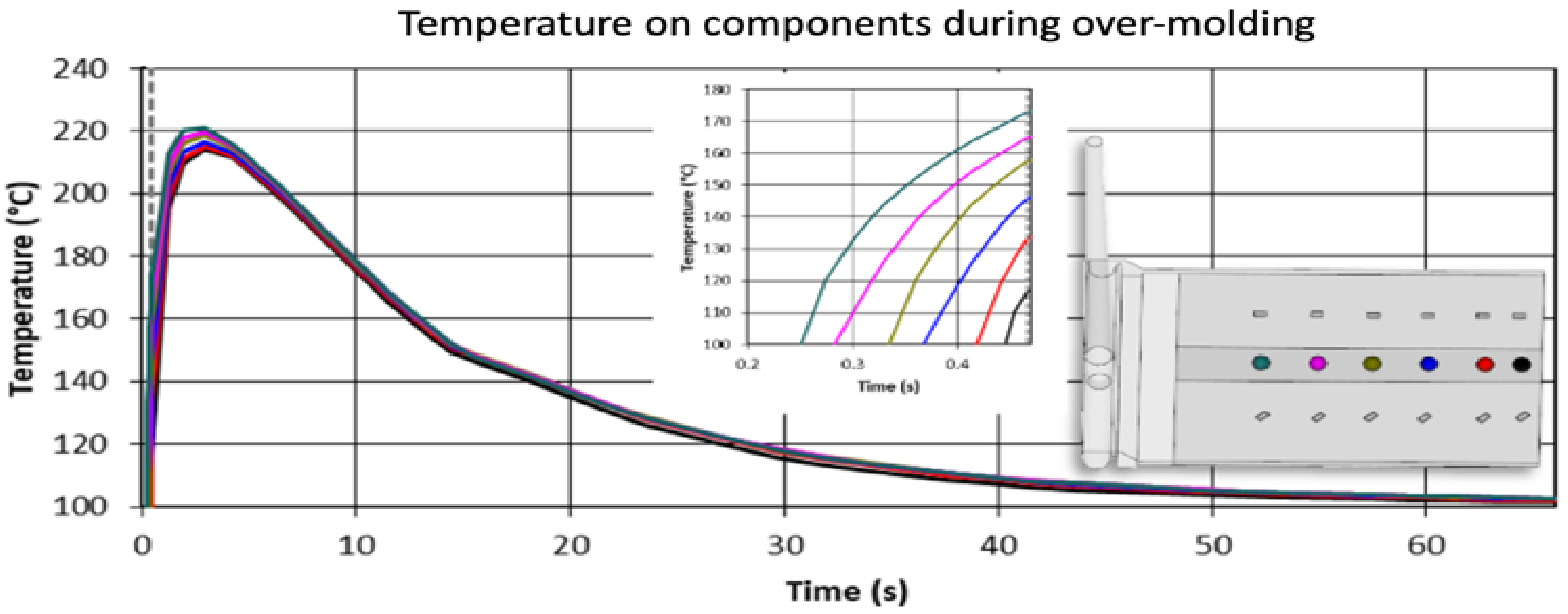
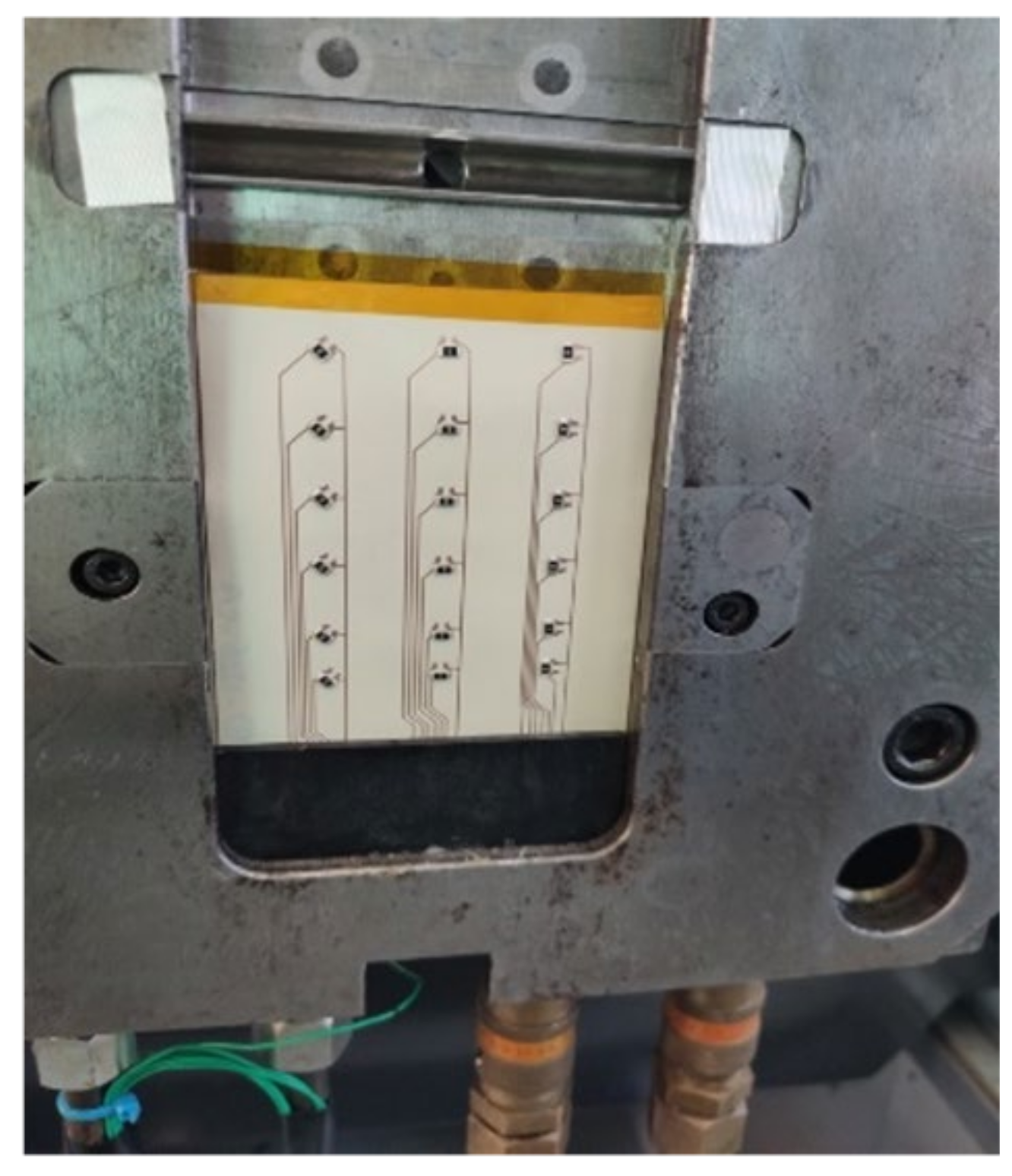
2.6. Over-Molding
3. Results
3.1. Shear Test
3.2. Foils Evaluation
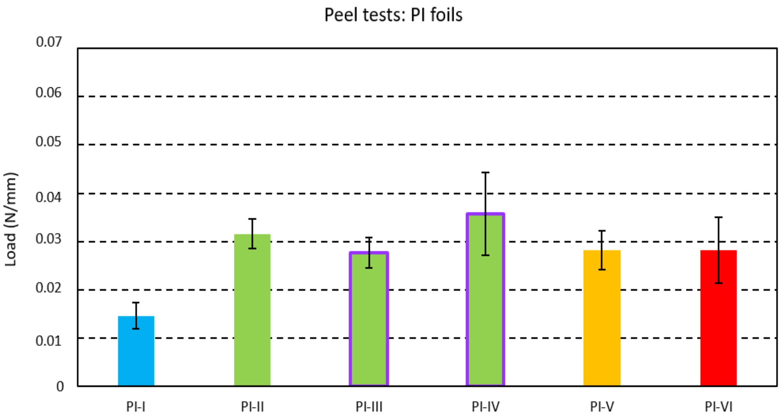
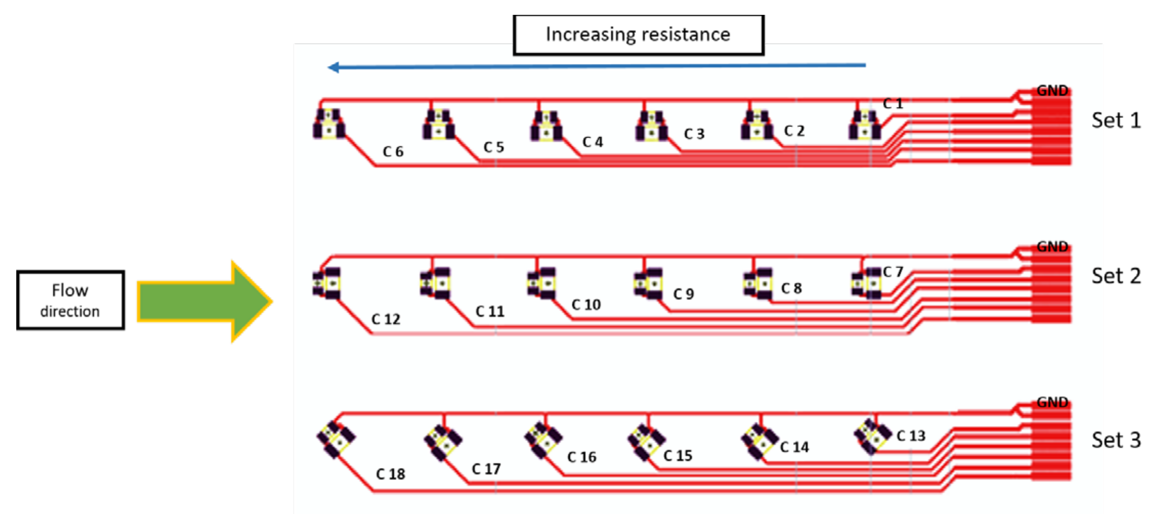
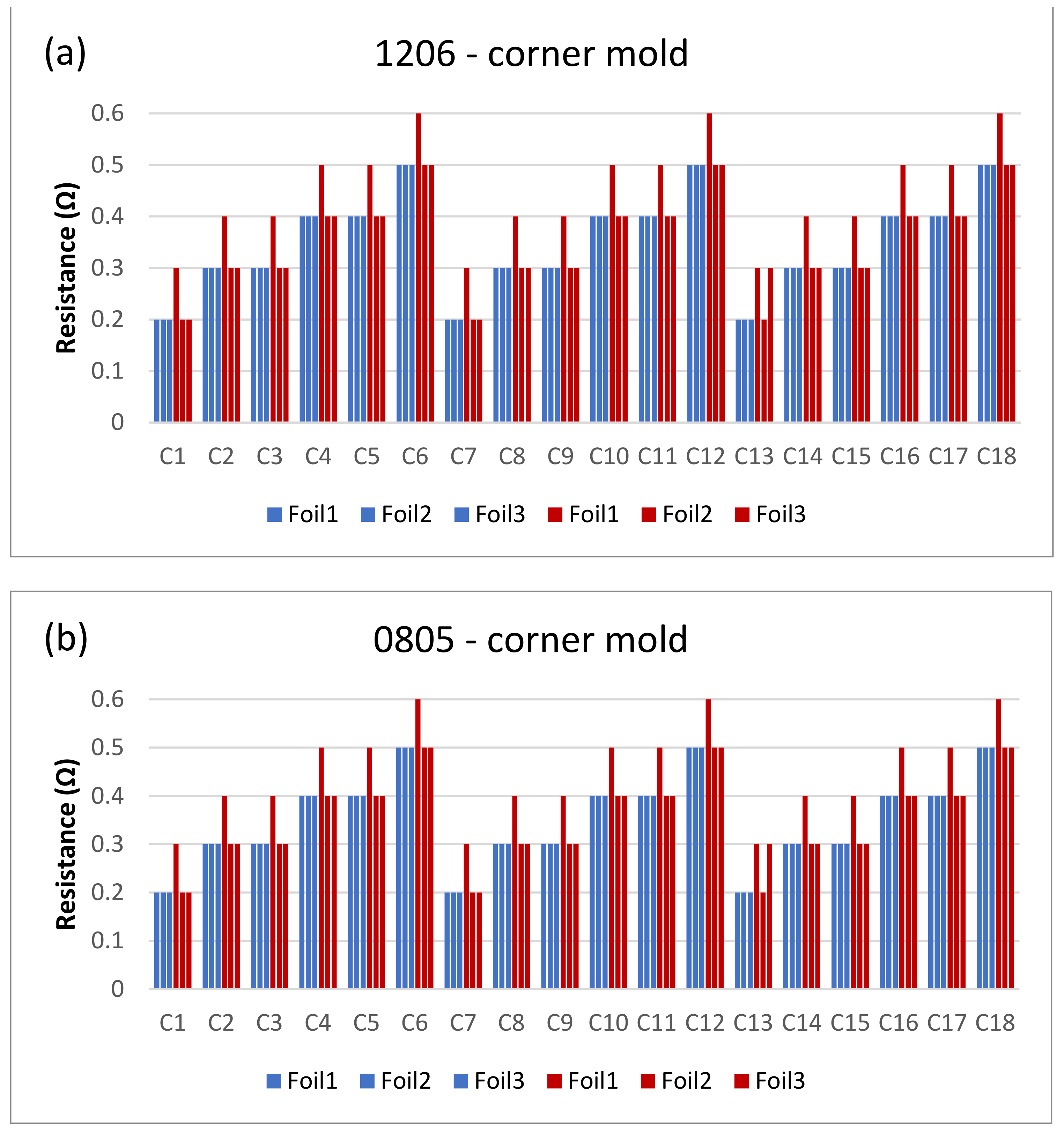
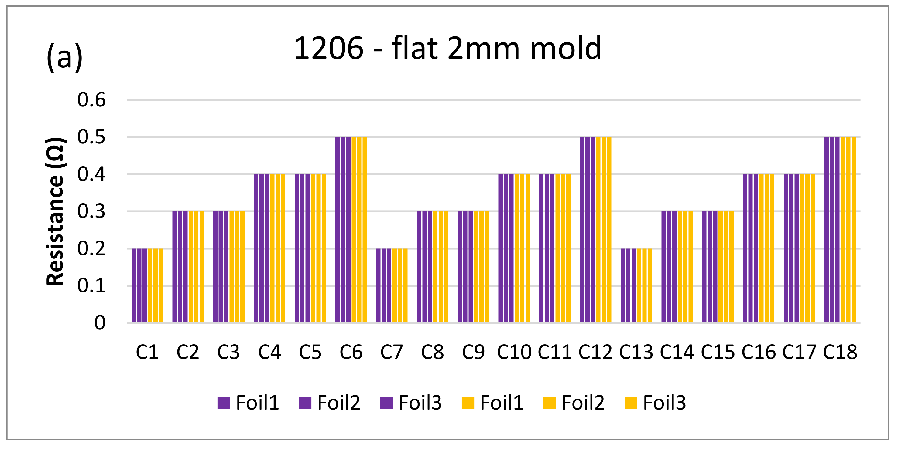
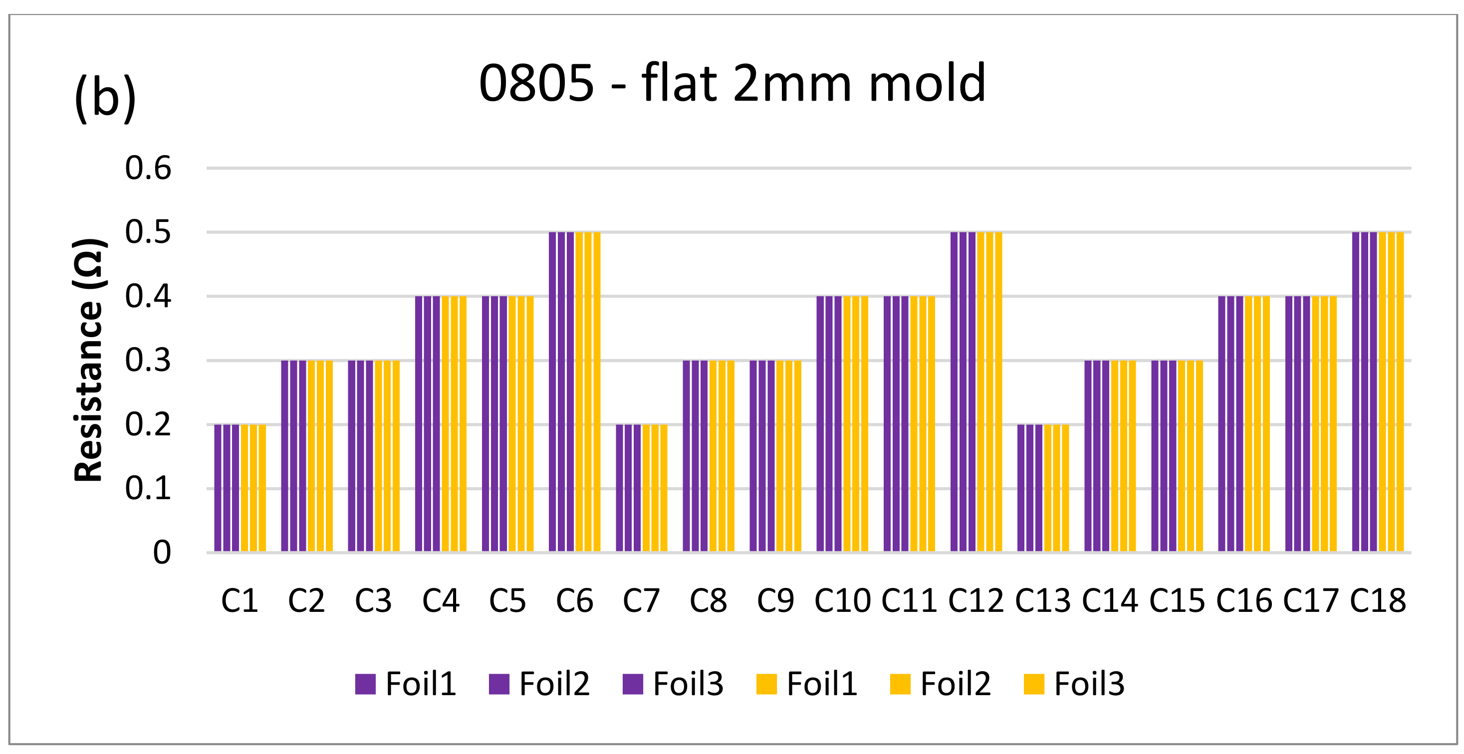
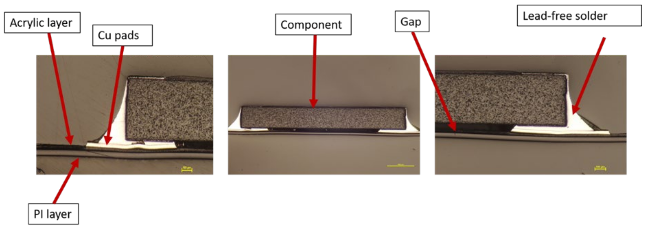
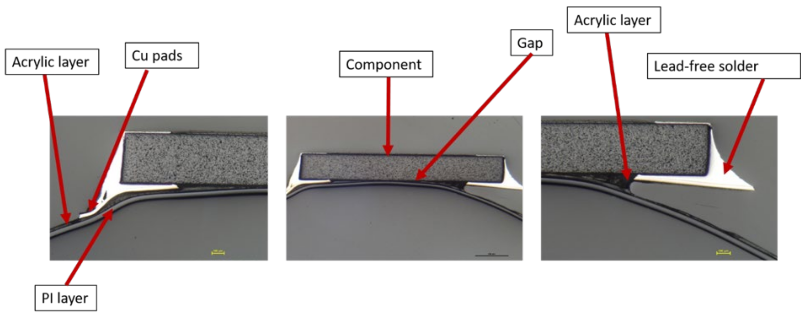
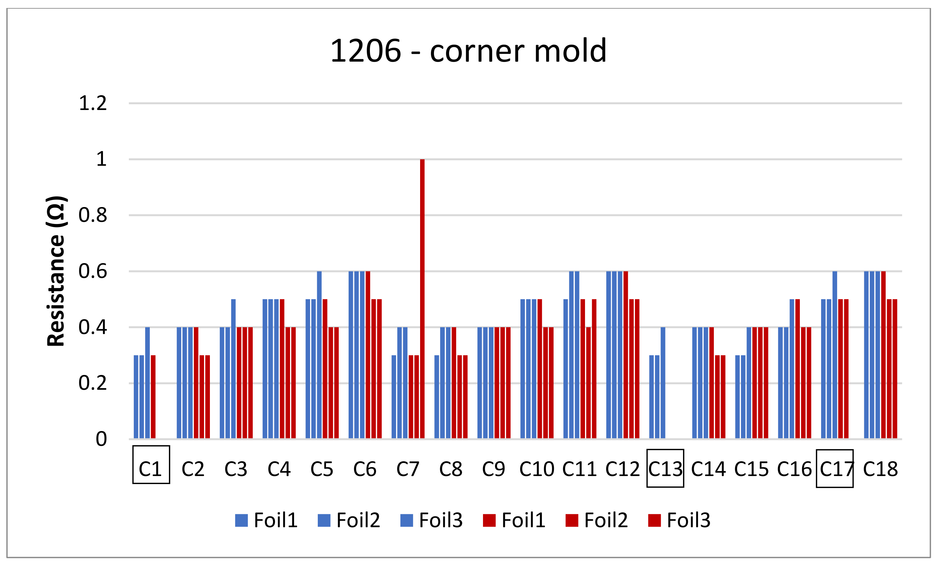
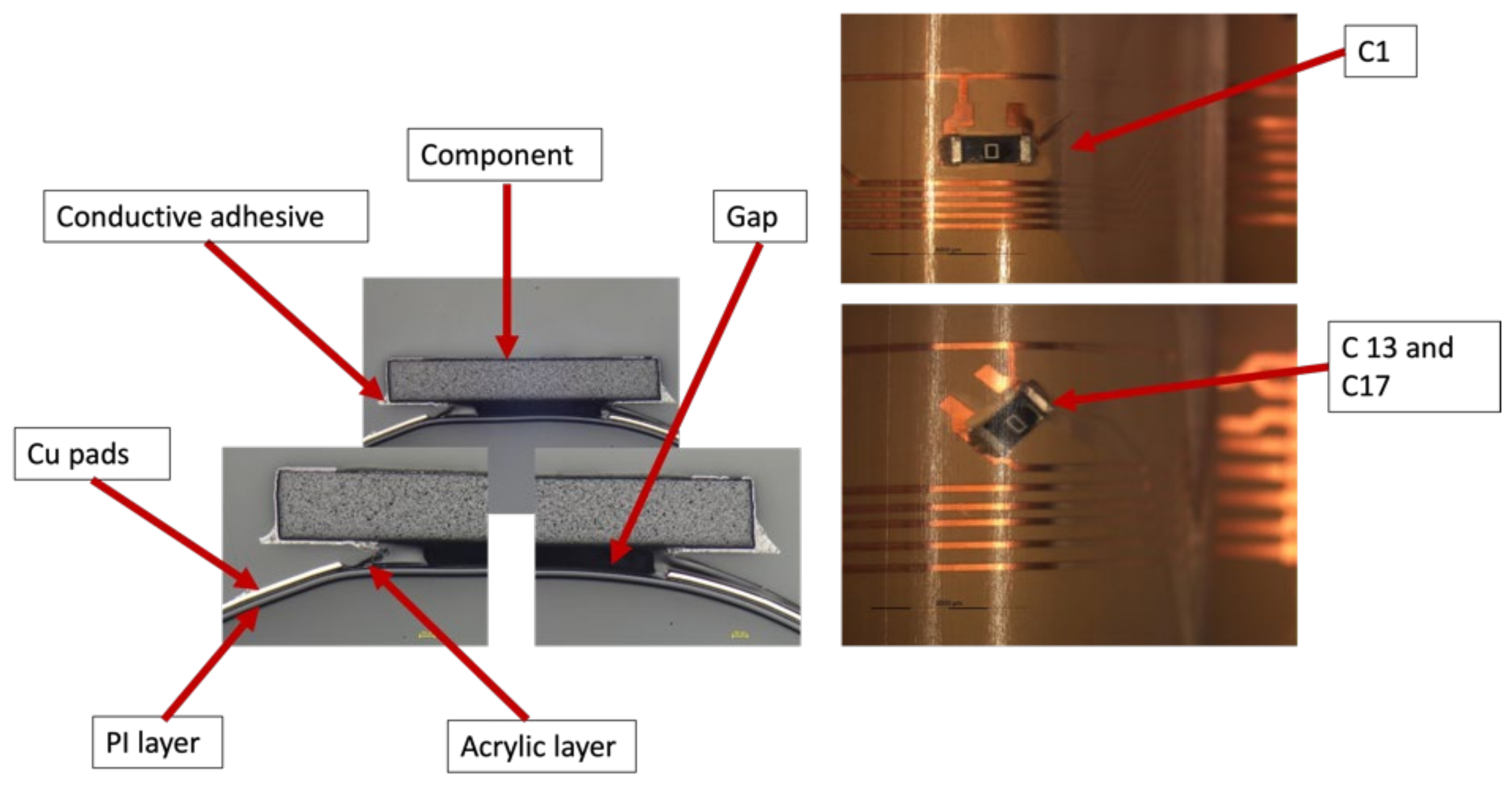
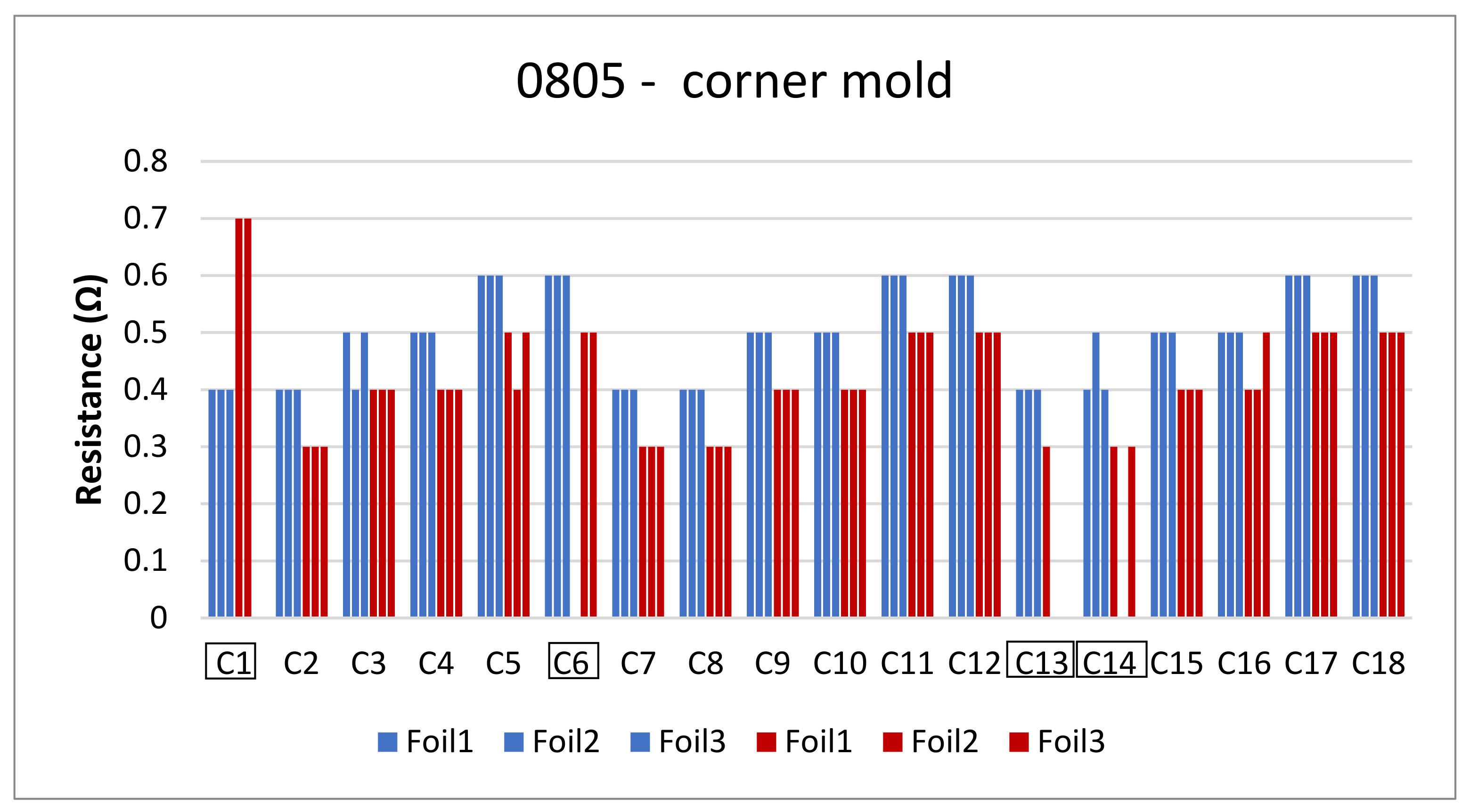
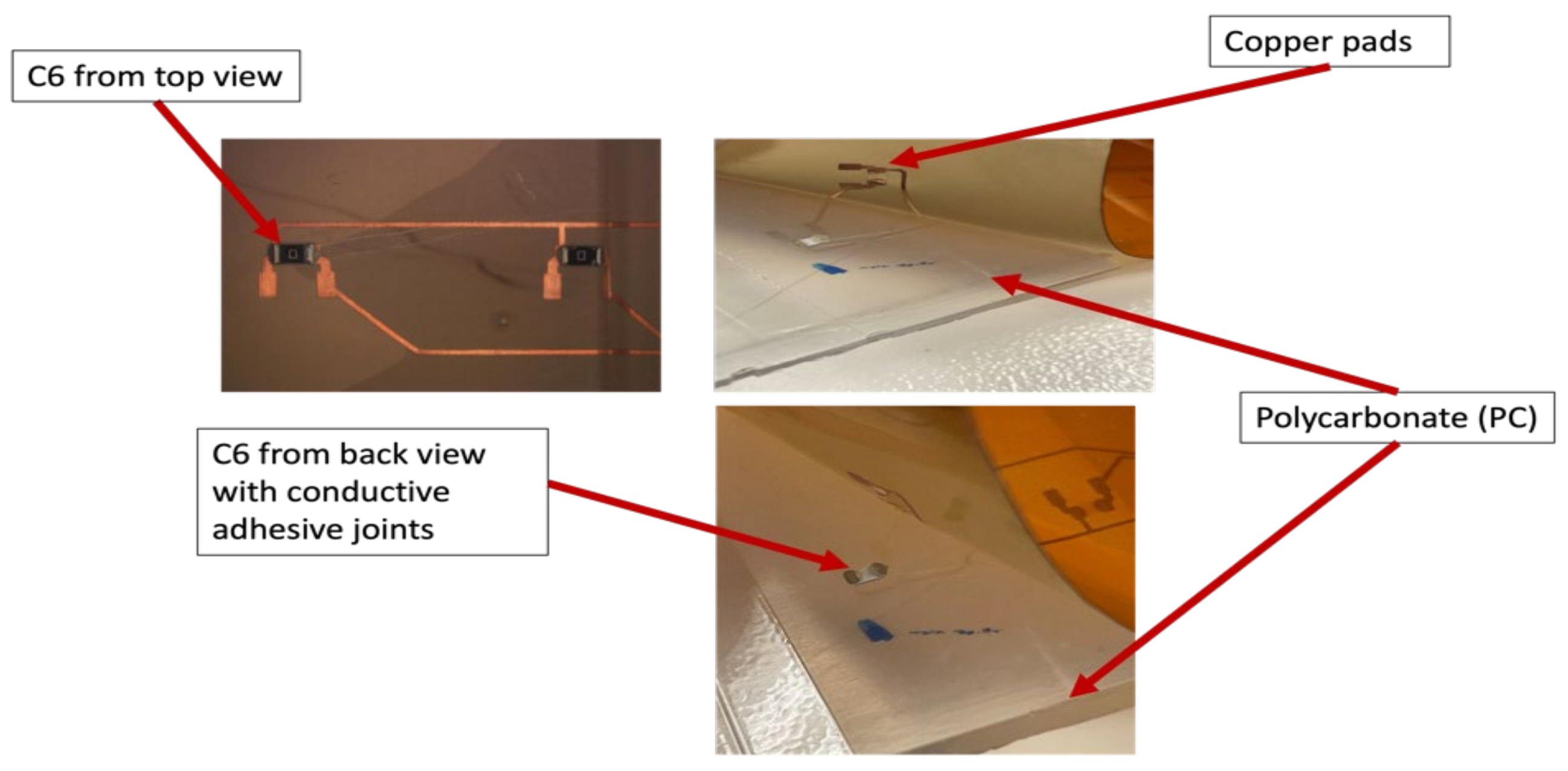
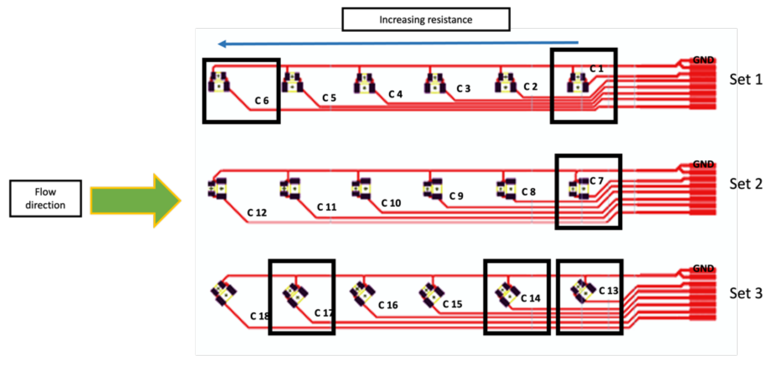
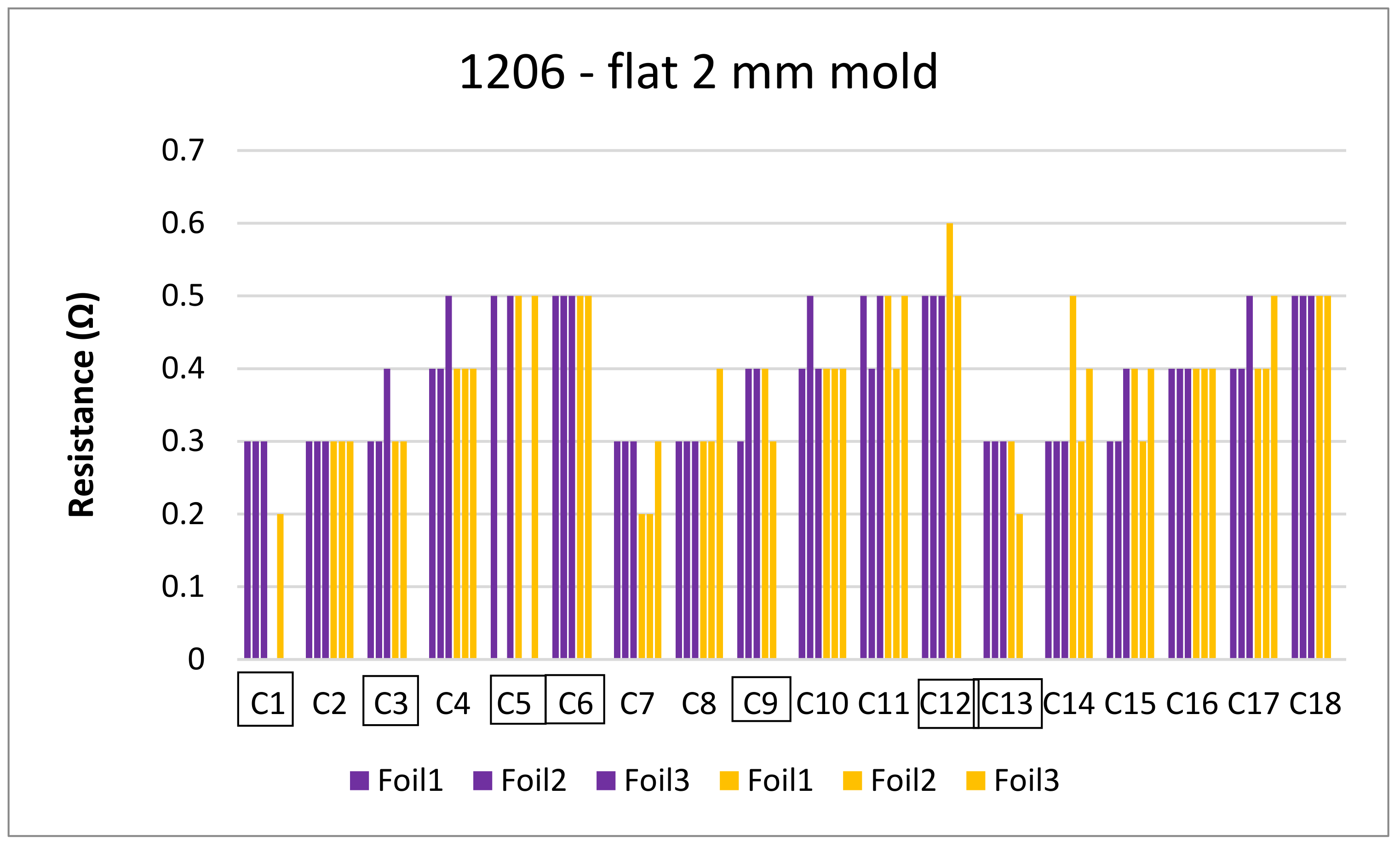
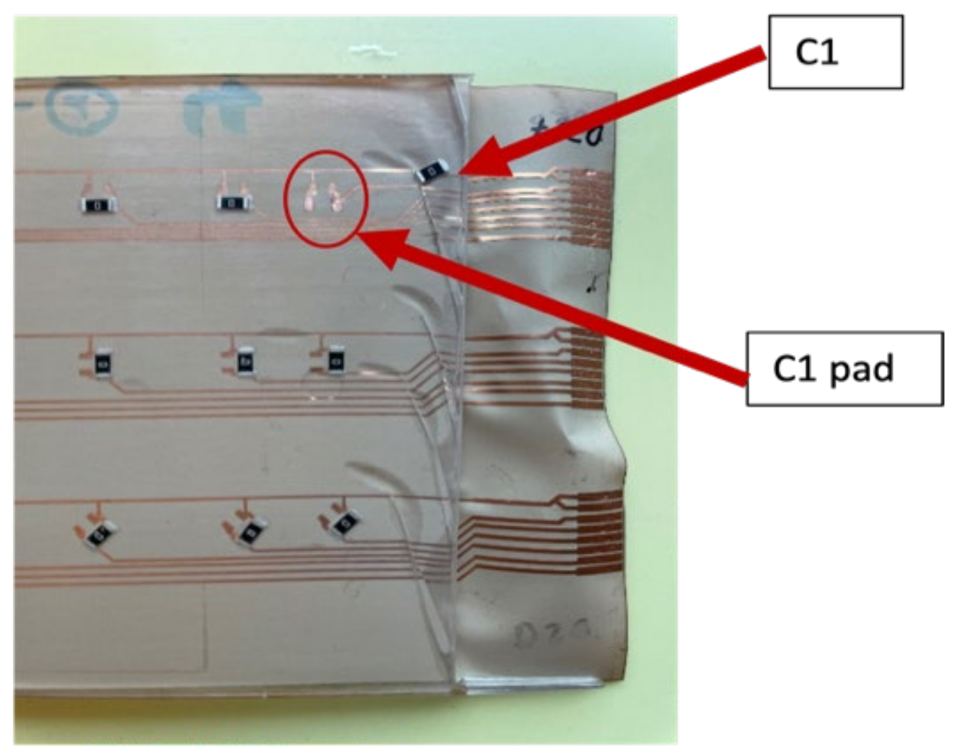
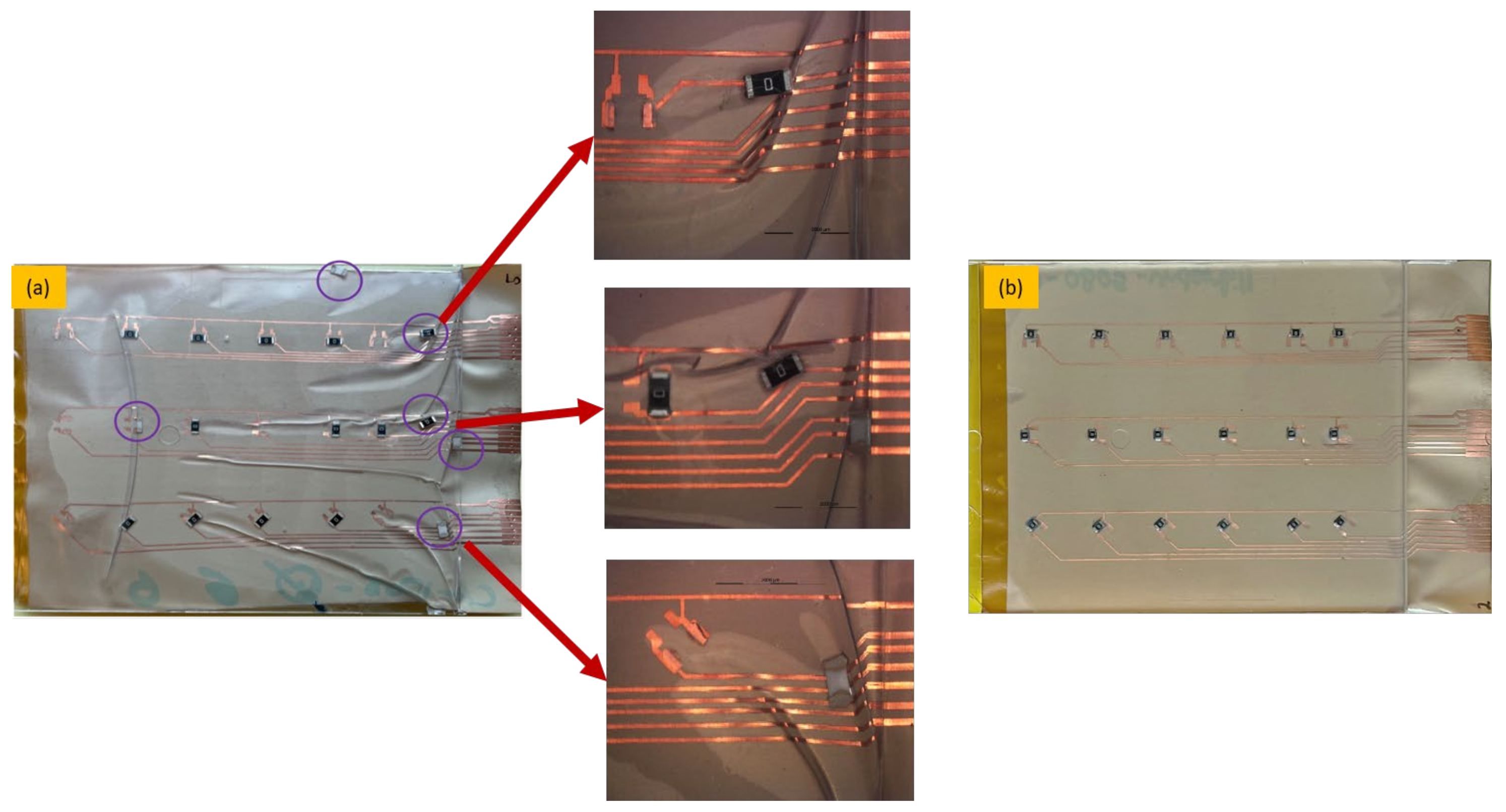
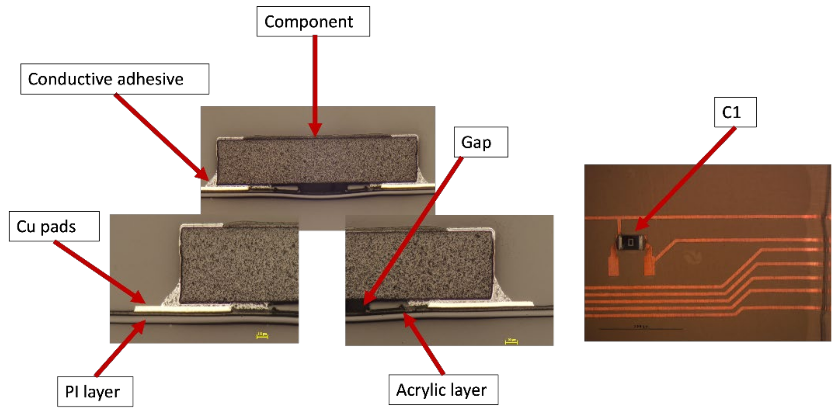
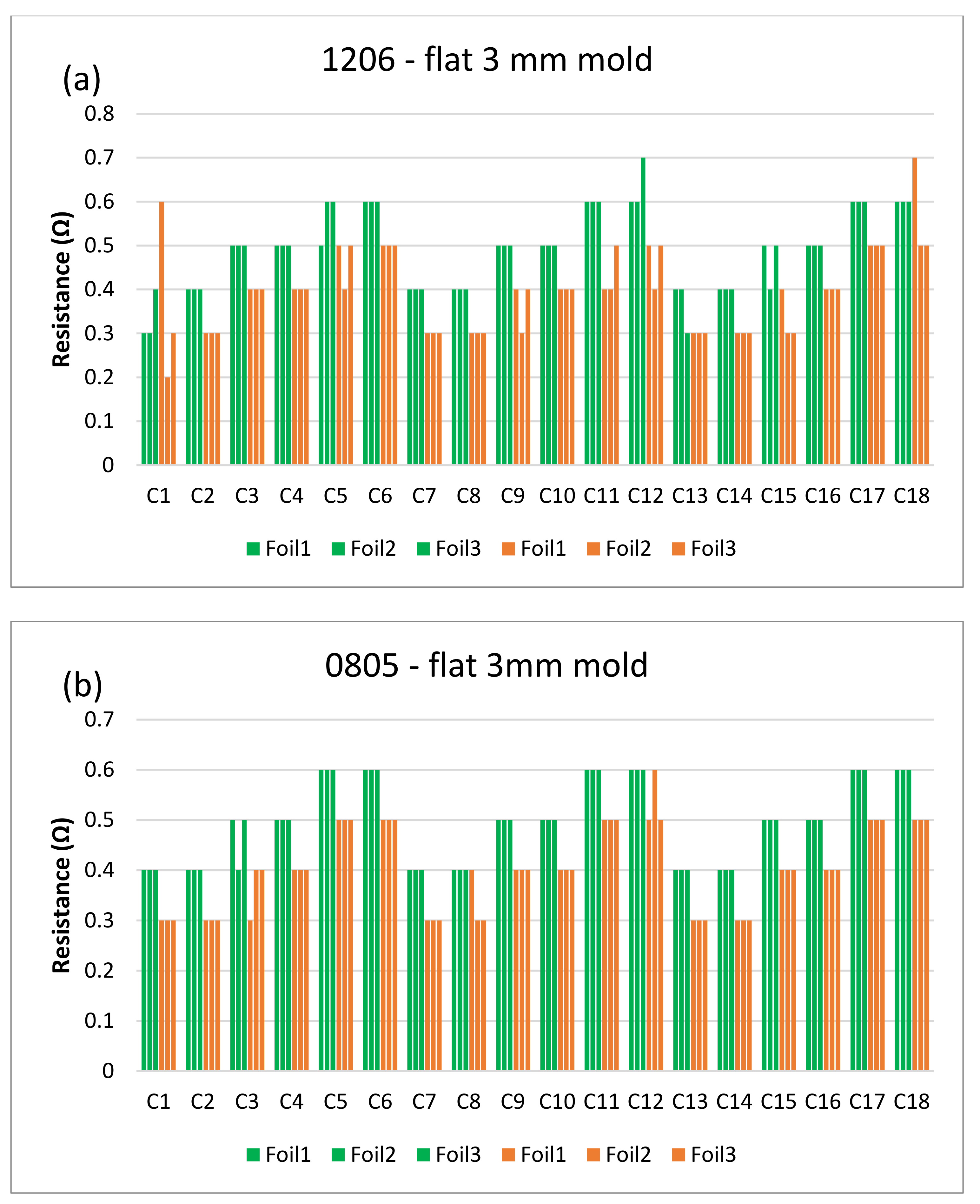
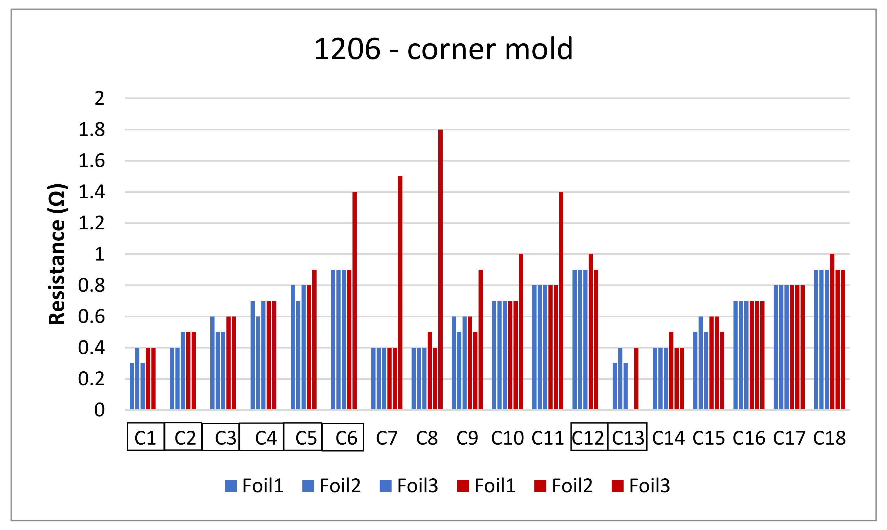
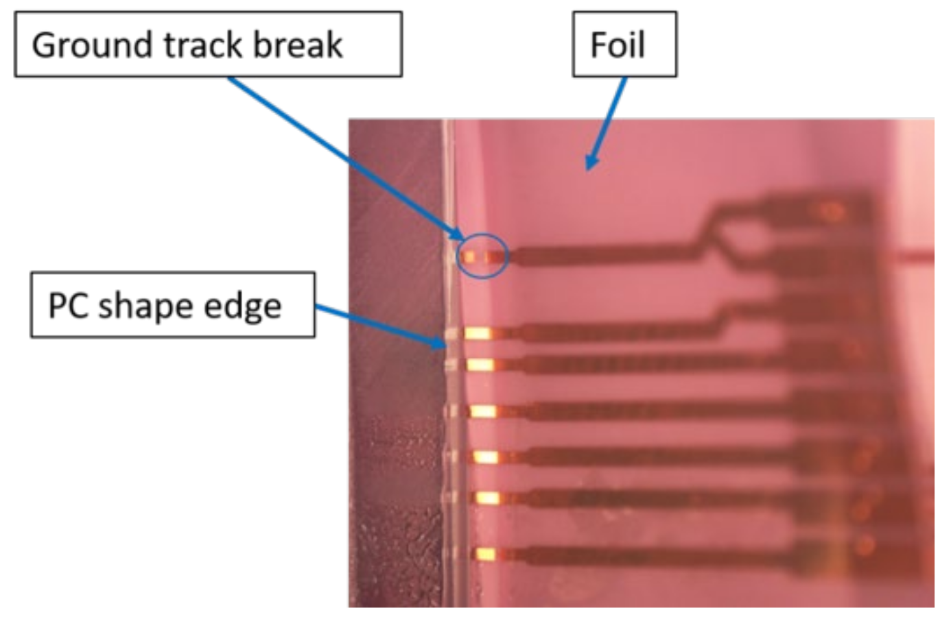
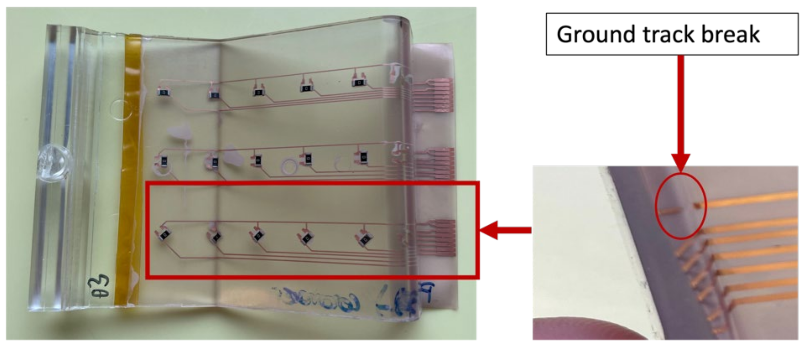
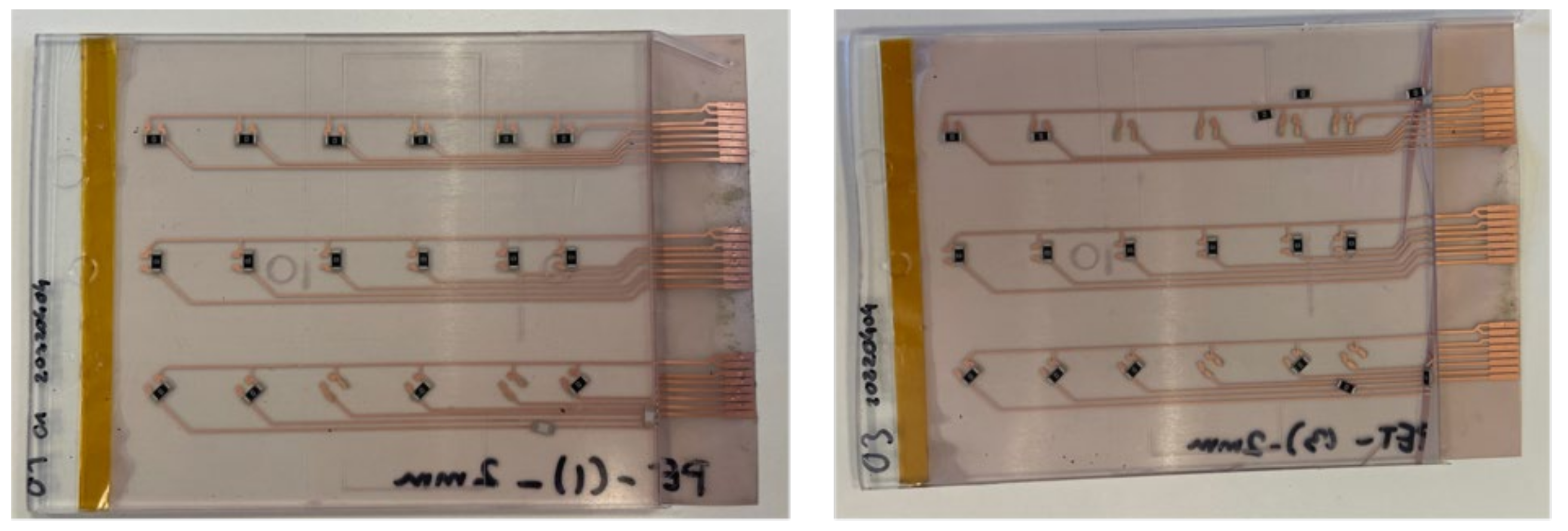
3.2.1. Measurements on PI-Cu Foils
Measurements on Samples Assembled with Lead-Free Solder
Measurements on Samples Assembled with Conductive Adhesive
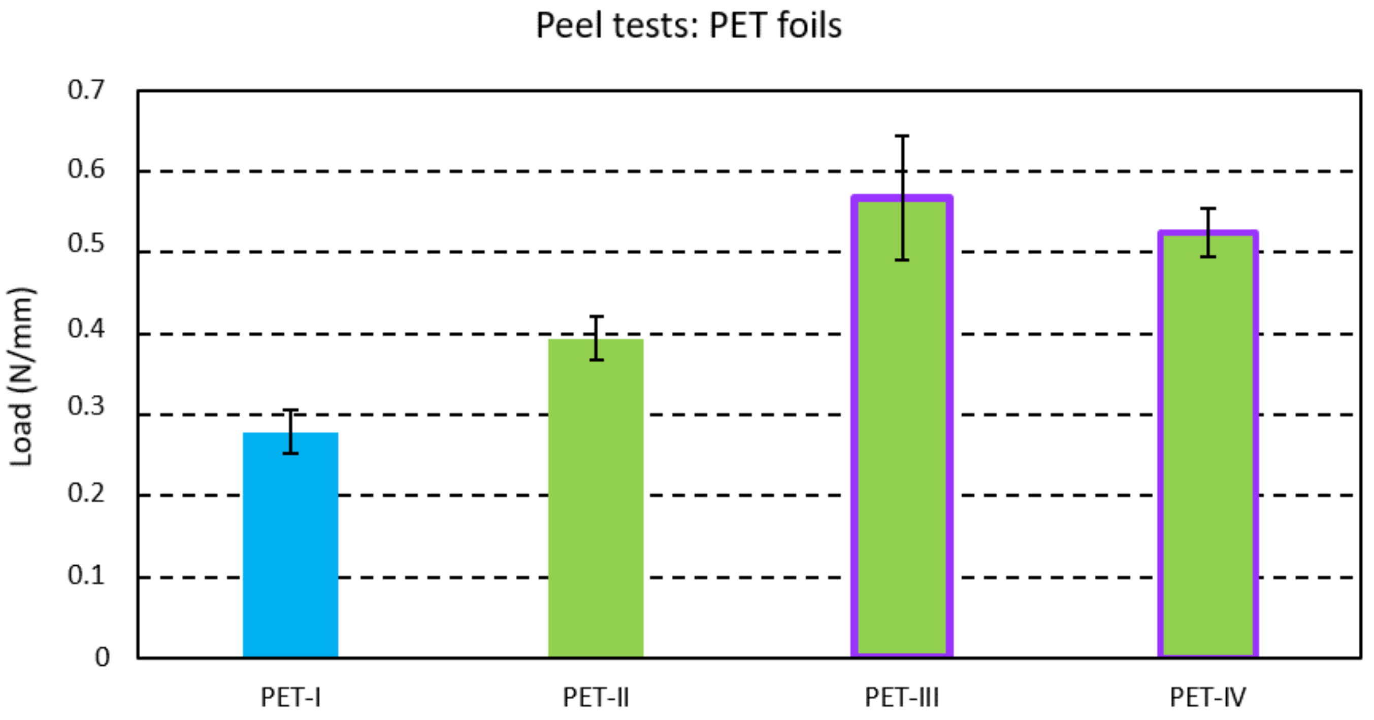
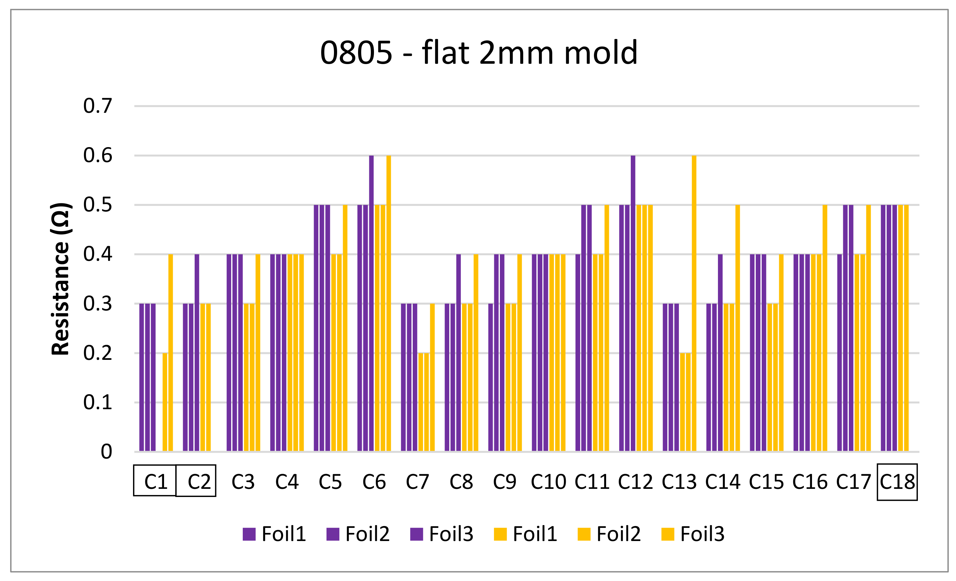
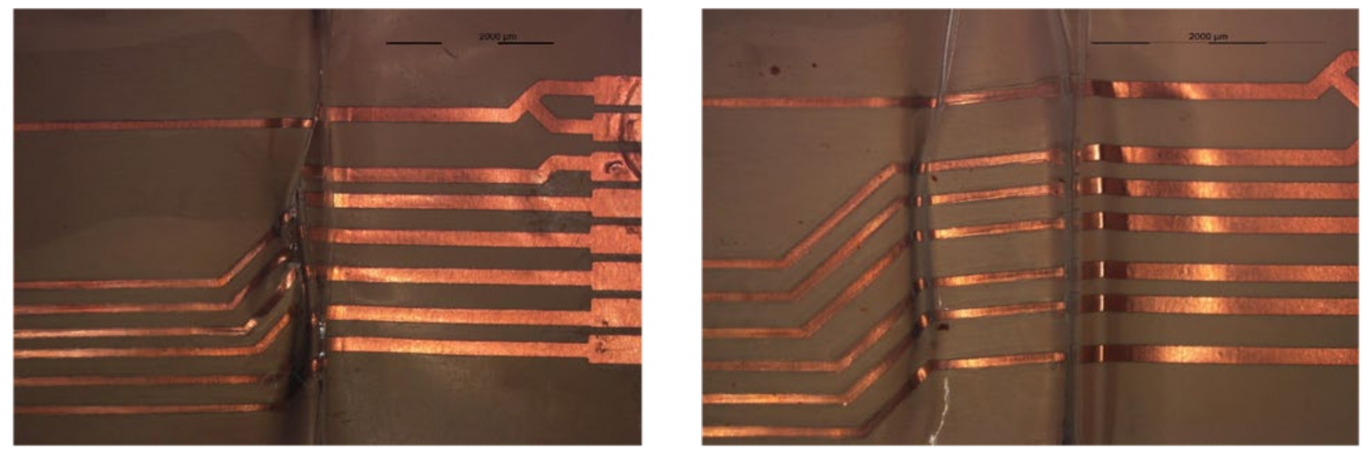
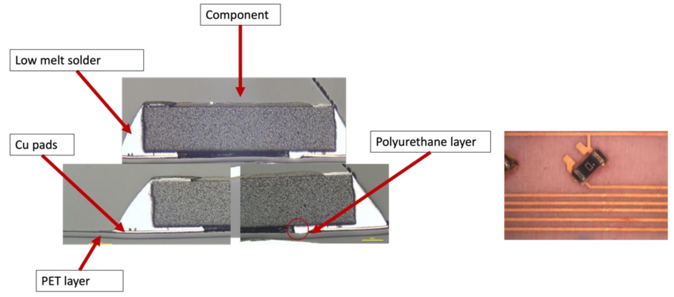
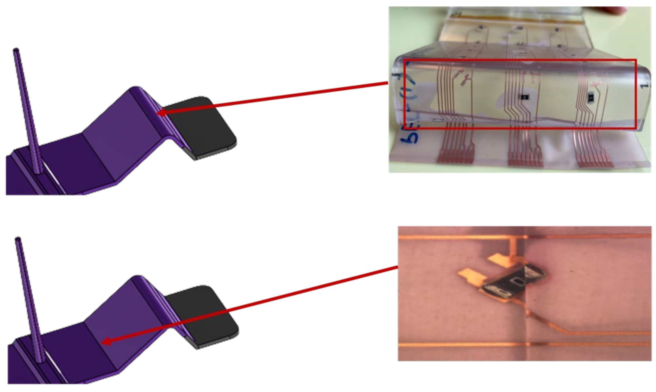
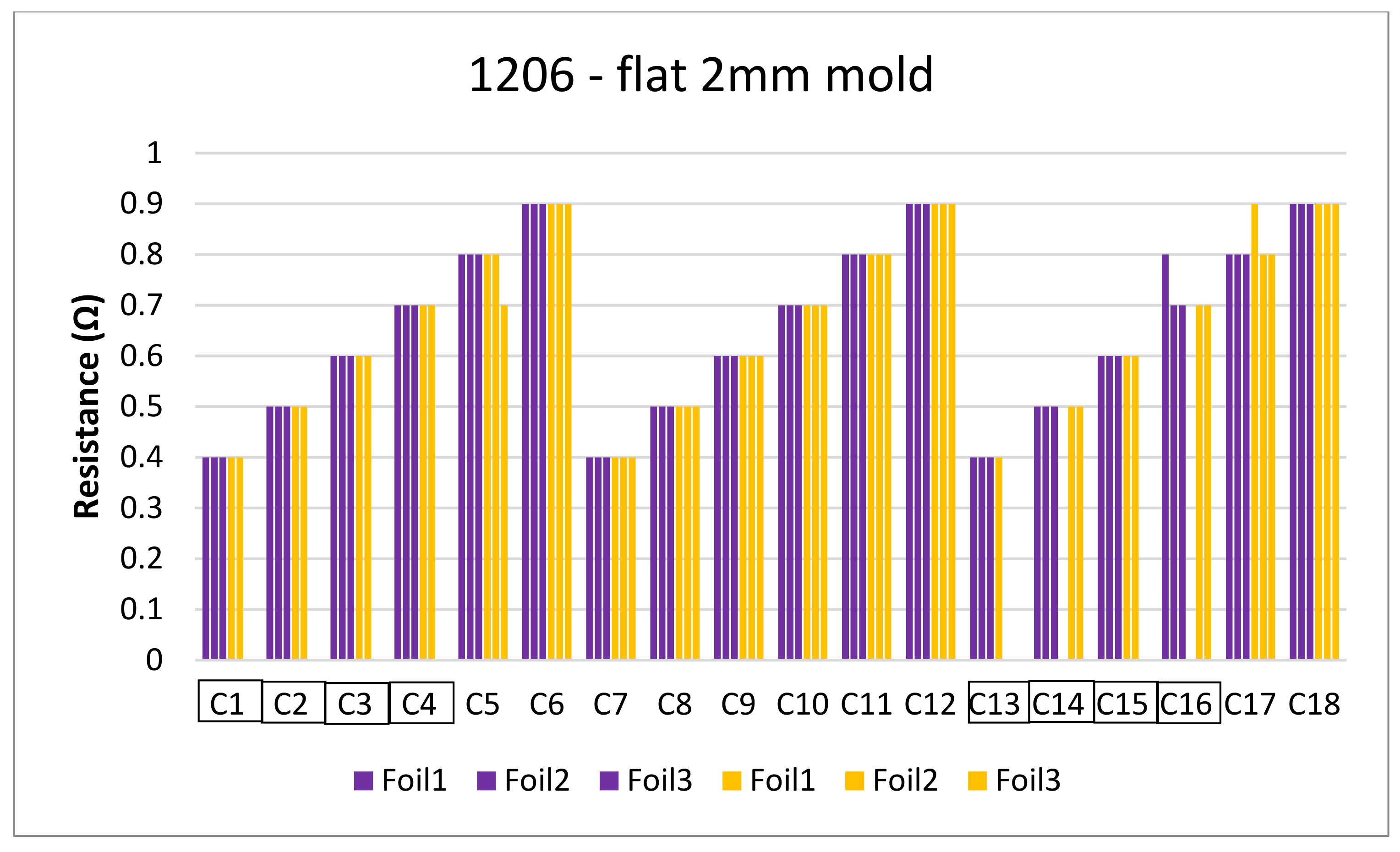
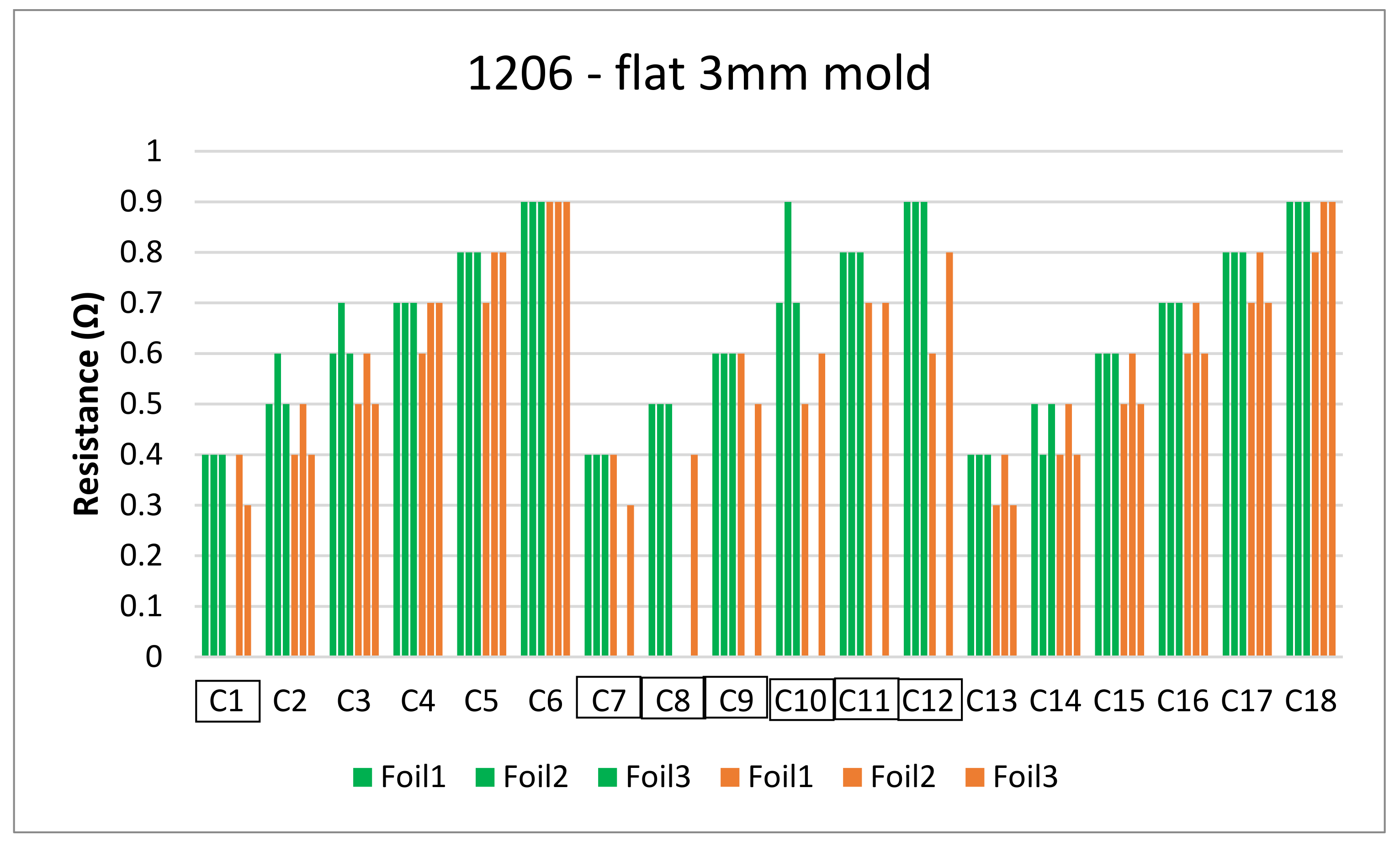
3.2.2. Measurements on PET-Cu Foils
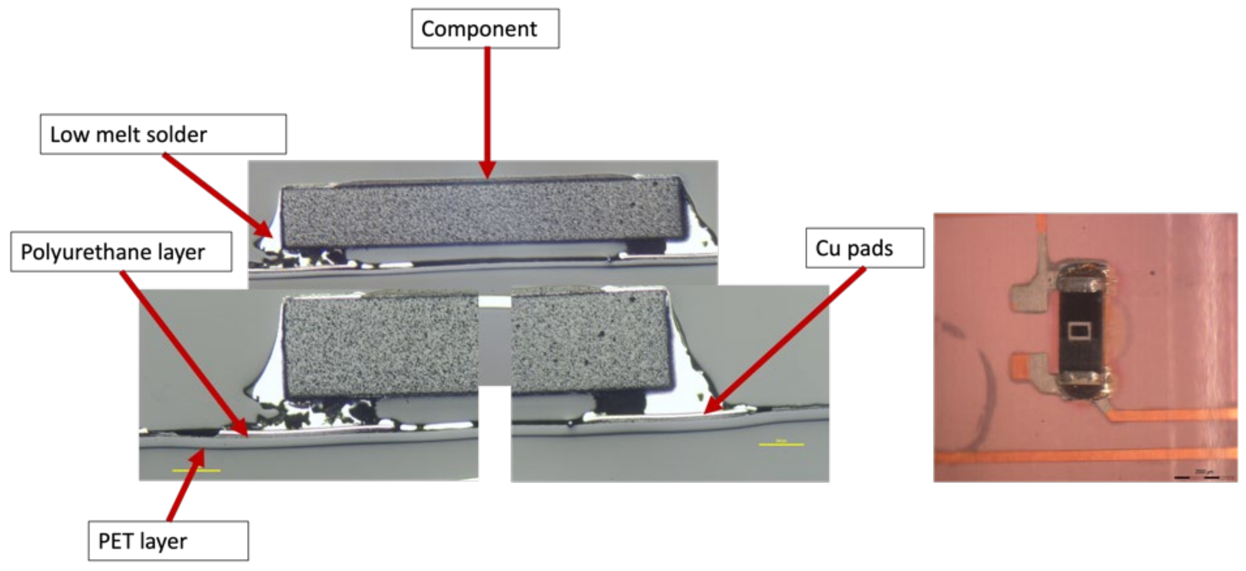
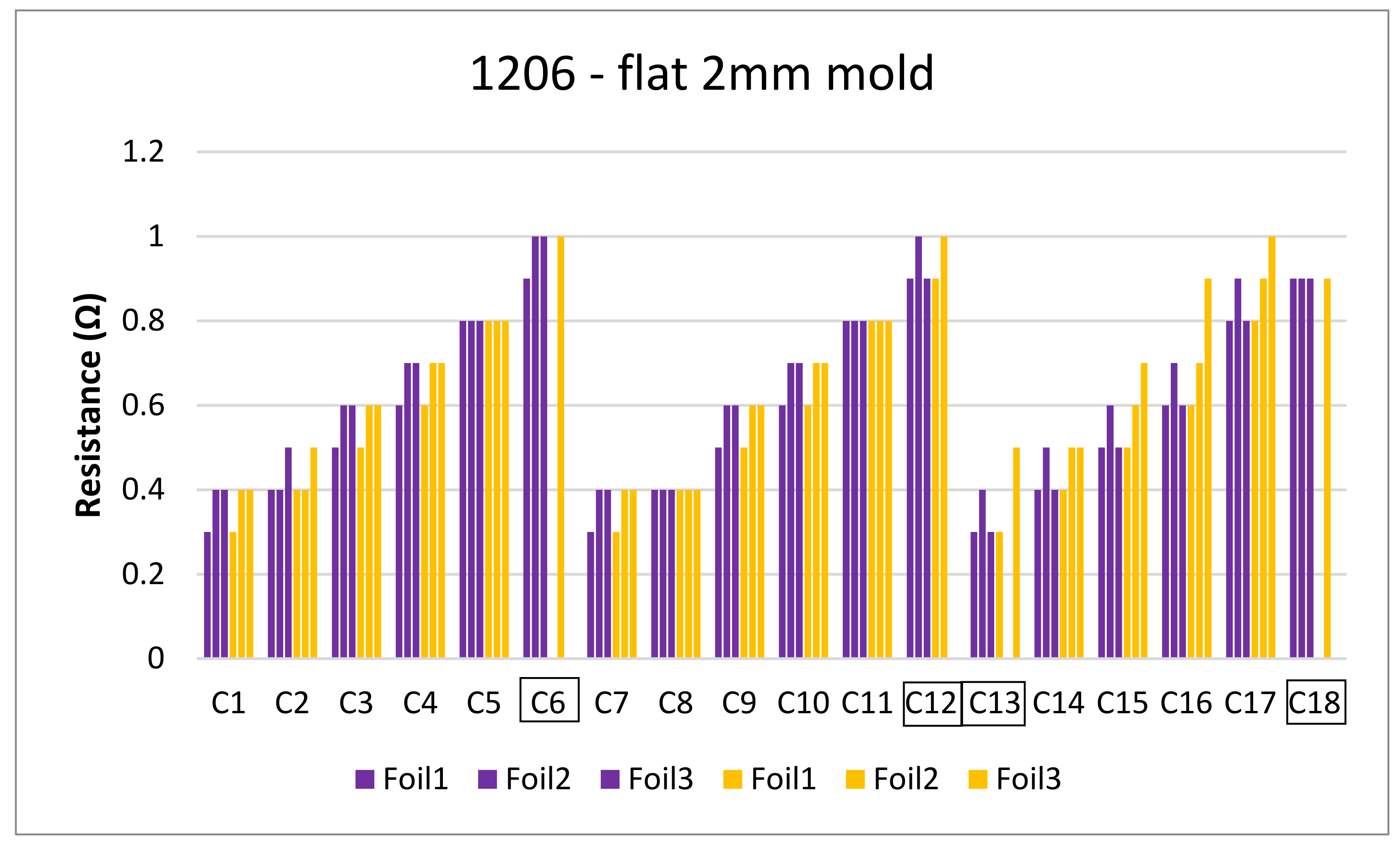
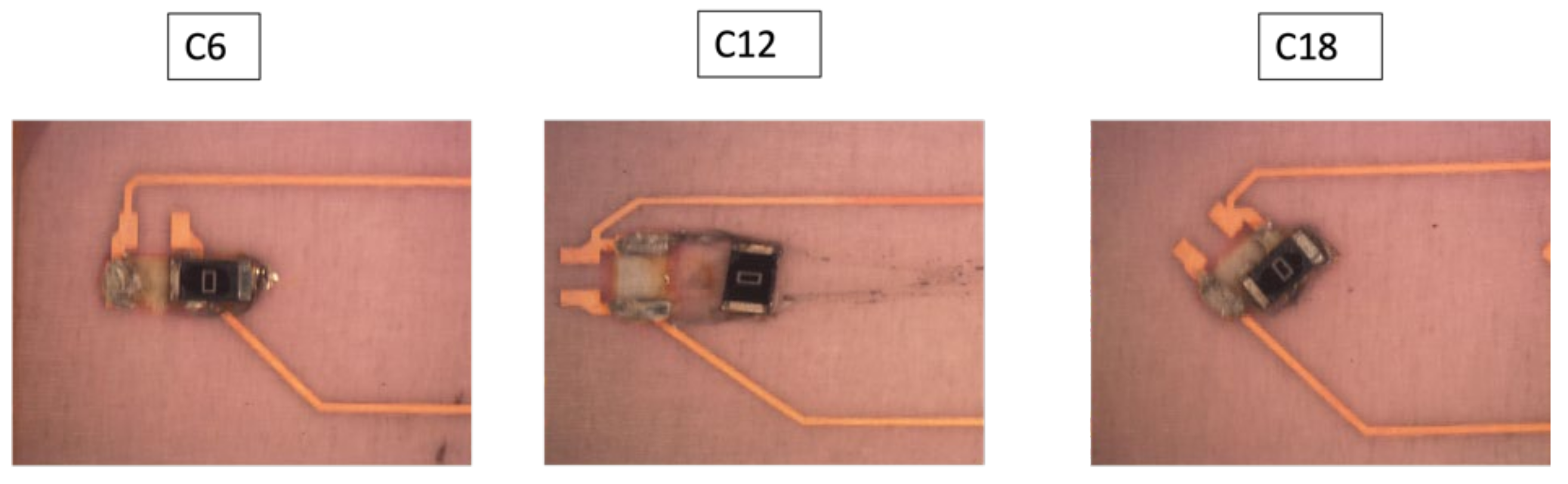
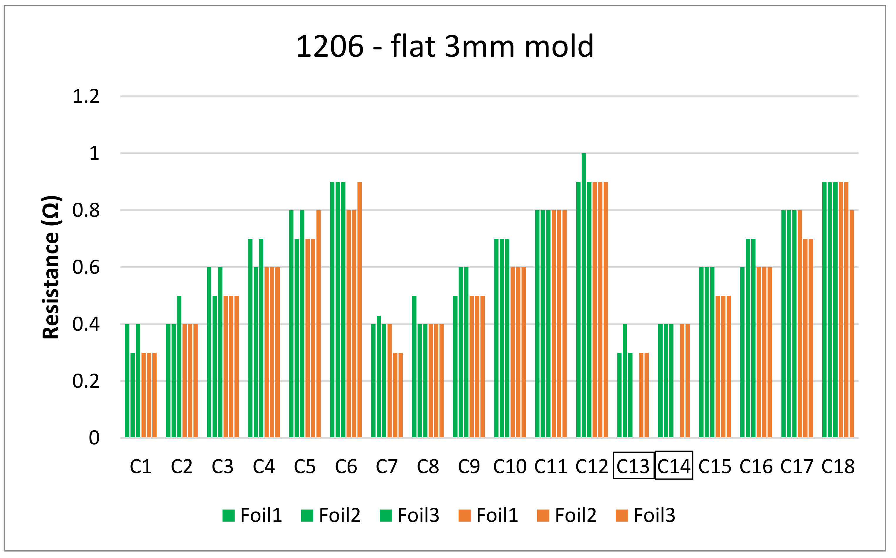
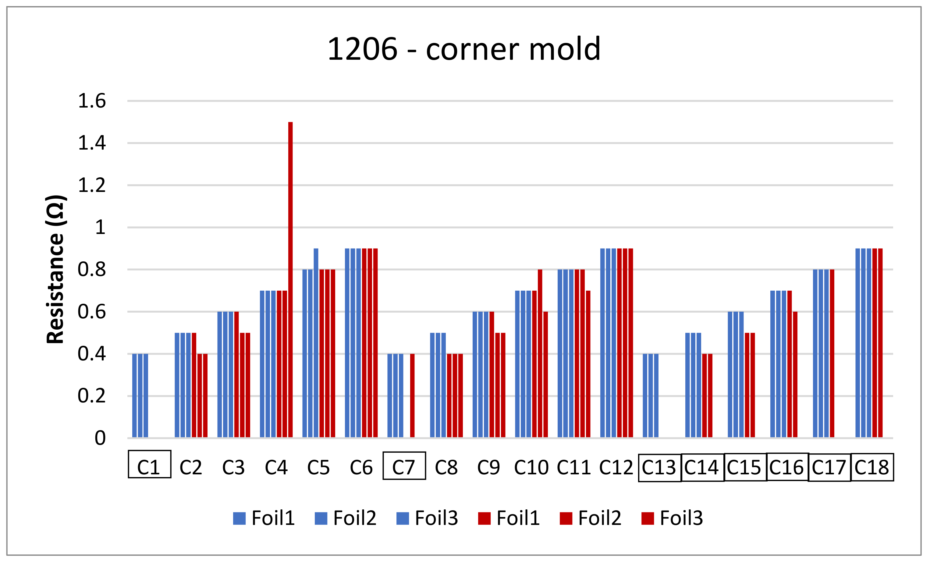
Measurements on Samples Assembled with Low-Temperature Solder
Measurements on Samples Assembled with Conductive Adhesive
4. Conclusion
Author Contributions
Funding
Institutional Review Board Statement
Informed Consent Statement
Data Availability Statement
Acknowledgments
Conflicts of Interest
References
- Pötsch, G.; Michaeli, W. Injection Molding: An Introduction; Carl Hanser Publishers: Munich, Germany, 2008. [Google Scholar]
- Singh, G.; Verma, A. A brief review on injection moulding manufacturing process. Mater. Today Proc. 2017, 4, 1423–1433. [Google Scholar]
- Teh, N.J.; Prosser, S.; Conway, P.P.; Palmer, P.J.; Kioul, A. Embedding of electronics within thermoplastic polymers using injection moulding technique. In Proceedings of the Twenty Sixth IEEE/CPMT International Electronics Manufacturing Technology Symposium (Cat. No.00CH37146), Santa Clara, CA, USA, 3 October 2000; pp. 10–18. [Google Scholar] [CrossRef]
- Bakr, M.; Bossuyt, F.; Vanfleteren, J. The integration of electronic circuits in plastics using injection technologies: A literature review. Flex. Print. Electron. 2022, 7, 023001. [Google Scholar] [CrossRef]
- Alajoki, T.; Matti, K.; Markus, T.; Mikko, H.; Antti, K.; Kimmo, K.; Jukka-Tapani, M.; Janne, A.; Kari, R. Hybrid in-mould integration for novel electrical and optical features in 3D plastic products. In Proceedings of the 4th Electronic System-Integration Technology Conference, Amsterdam, Netherlands, 17–20 September 2012; pp. 1–6. [Google Scholar] [CrossRef]
- Rusanen, O.; Simula, T.; Niskala, P.; Lindholm, V.; Heikkinen, M. Injection Molded Structural Electronics Brings Surfaces to Life. In Proceedings of the 2019 22nd European Microelectronics and Packaging Conference & Exhibition (EMPC), Pisa, Italy, 16–19 September 2019; pp. 1–7. [Google Scholar] [CrossRef]
- Juntunen, E.; Ihme, S.; Huttunen, A.; Mäkinen, J. R2R process for integrating LEDs on flexible substrate. In Proceedings of the 2017 IMAPS Nordic Conference on Microelectronics Packaging (NordPac), Gothenburg, Sweden, 18–20 June 2017; pp. 12–16. [Google Scholar] [CrossRef]
- Kololuoma, T.; Keränen, M.; Kurkela, T.; Happonen, T.; Korkalainen, M.; Kehusmaa, M.; Gomes, L.; Branco, A.; Ihme, S.; Pinheiro, C.; et al. Adopting Hybrid Integrated Flexible Electronics in Products: Case—Personal Activity Meter. IEEE J. Electron Devices Soc. 2019, 7, 761–768. [Google Scholar] [CrossRef]
- Bakr, M.; Bauwens, P.; Bossuyt, F.; Vanfleteren, J.; Chtioui, I.; Christiaens, W. Solar cells integration in over-molded printed electronics. In Proceedings of the 2020 IEEE 8th Electronics System-Integration Technology Conference (ESTC), Tønsberg, Norway, 15–18 September 2020; pp. 1–5. [Google Scholar] [CrossRef]
- Bakr, M.; Bossuyt, F.; Vanfleteren, J.; Su, Y. Flexible Microsystems Using Over-molding Technology. Procedia Manuf. 2020, 52, 26–31. [Google Scholar] [CrossRef]
- Wimmer, A.; Reichel, H.; Schmidt, S. New standards for 3D-userinterfaces-manufactured by a Film Insert Molding process. In Proceedings of the 2018 13th International Congress Molded Interconnect Devices (MID), Würzburg, Germany, 25–26 September 2018; pp. 1–5. [Google Scholar] [CrossRef]
- Gbotemi, O.; Myllymäki, S.; Jantunen, H.; Juuti, J.; Ihme, S.; Kurkinen, M.; Majava, V.; Tuhkala, M.; Kemppainen, J. Printed GNSS and Bluetooth Antennas Embedded on Flexible Low Loss Substrates for Wearable Applications. Prog. Electromagn. Res. M 2020, 94, 189–199. [Google Scholar] [CrossRef]
- Tuomikoski, M.; Ihme, S.; Huttunen, A.; Korkalainen, M.; Yrjänä, S. Indoor air quality sensing indicators. In Proceedings of the 2016 6th Electronic System-Integration Technology Conference (ESTC), Grenoble, France, 13–15 September 2016; pp. 1–6. [Google Scholar] [CrossRef]
- Nguyen, S.; Perez, C.J.; Desimone, M.; Pastor, J.M.; Tomba, J.P.; Carellaa, J.M. Adhesion control for injection overmolding of elastomeric propylene copolymers on polypropylene. Effects of block and random microstructures. Int. J. Adhes. Adhes. 2013, 46, 44–55. [Google Scholar] [CrossRef]
- Stan, F.; Fetecau, C. Experimental Investigation of the Adhesion Between Thermoplastic Polyurethane and Acrylonitrile-Butadiene-Styrene Substrate. In Proceedings of the ASME 2014 International Manufacturing Science and Engineering Conference collocated with the JSME 2014 International Conference on Materials and Processing and the 42nd North American Manufacturing Research Conference. Volume 2: Processing, Detroit, MI, USA, 9–13 June 2014. [Google Scholar] [CrossRef]
- Ott, C.; Wolf, M.; Drummer, D. Media-Tight Polymer-Polymer Assemblies By Means of Sintered Powder Layer in Assembly Injection Moulding. Procedia Manuf. 2020, 47, 362–367. [Google Scholar] [CrossRef]
- Leong, Y.W.; Ishiaku, U.S.; Kotaki, M.; Hamada, H.; Yamaguchi, S. Interfacial characteristics of film insert molded polycarbonate film/polycarbonate-acrylonitrile-butadiene-styrene substrate, part 1: Influence of substrate molecular weight and film thickness. Polym. Eng. Sci. 2006, 46, 1674–1683. [Google Scholar] [CrossRef]
- Leong, Y.W.; Ishiaku, U.S.; Kotaki, M.; Hamada, H.; Yamaguchi, S. Effect of crystallization and interface formation mechanism on mechanical properties of film-insert injection-molded poly(propylene) (PP) film/PP substrate. J. Appl. Polym. Sci. 2005, 98, 294–301. [Google Scholar]
- Chen, S.C.; Li, H.M.; Huang, S.T.; Wang, Y.C. Effect of decoration film on mold surface temperature during in-mold decoration injection molding process. Int. Commun. Heat Mass Transf. 2010, 37, 501–505. [Google Scholar] [CrossRef]
- Chen, H.L.; Chen, S.C.; Liao, W.H.; Chien, R.D.; Lin, Y.T. Effects of insert film on asymmetric mold temperature and associated part warpage during in-mold decoration injection molding of PP parts. Int. Commun. Heat Mass Transf. 2013, 41, 34–40. [Google Scholar] [CrossRef]
- Baldan, A. Adhesion phenomena in bonded joints. Int. J. Adhes. Adhes. 2012, 38, 95–116. [Google Scholar] [CrossRef]
- Awaja, F.; Gilbert, M.; Kelly, G.; Fox, B.; Pigram, P.J. Adhesion of polymers. Prog. Polym. Sci. 2009, 34, 948–968. [Google Scholar] [CrossRef]
- Creton, C.; Kramer, E.J.; Brown, H.R.; Hui, C.Y. Adhesion and Fracture of Interfaces Between Immiscible Polymers: From the Molecular to the Continuum Scal. In Molecular Simulation Fracture Gel Theory; Springer: Berlin/Heidelberg, Germany, 2001; pp. 53–136. [Google Scholar]
- Cole, P.J.; Cook, R.F.; Macosko, C.W. Adhesion between immiscible polymers correlated with interfacial entanglements. Macromolecules 2003, 36, 2808–2815. [Google Scholar] [CrossRef]
- Available online: https://www.campusplastics.com/campus/de/datasheet/Makrolon%C2%AE+2805/Covestro+Deutschland+AG/22/7541f4aa (accessed on 29 September 2022).
- LeGrand, D.G.; Bendler, J.T. Plastics engineering, Bd. 56. In Handbook of Polycarbonate Science and Technology; Marcel Dekker: New York, NY, USA, 2000. [Google Scholar]
- Available online: https://www.dupont.com/content/dam/dupont/amer/us/en/products/ei-transformation/documents/EI-10113-Pyralux-FR-CCL-Data-Sheet.pdf (accessed on 29 September 2022).
- Available online: https://www.gtsflexible.com/product-table/?tx_gtsproducts_products%5Baction%5D=list&tx_gtsproducts_products%5Bcontroller%5D=Products&cHash=b0ee19a0fdbc58db79b019bffba1c77c#productList (accessed on 29 September 2022).
- Available online: https://www.professionalplastics.com/professionalplastics/content/AcryliteFFDataSheet.pdf (accessed on 29 September 2022).
- Bath, J. Lead-Free Soldering; Springer: New York, NY, USA, 2007. [Google Scholar]
- Available online: https://www.henkel-adhesives.com/be/en/product/electrically-conductiveadhesives/loctite_ablestikce3103wlv.html (accessed on 29 September 2022).
- Available online: https://interflux.com/en/product/DP-5600 (accessed on 29 September 2022).
- Wimmer, A.; Reichel, H.; Rauch, B.; Schramm, R.; Hörber, J.; Hä:ßler, B. Manufacturing of sandwich structures for the integration of electronics in in mold labelling components. In Proceedings of the 2016 12th International Congress Molded Interconnect Devices (MID), Wuerzburg, Germany, 28–29 September 2016; pp. 1–4. [Google Scholar] [CrossRef]
- Alajoki, T.; Koponen, M.; Juntunen, E.; Petaja, J.; Heikkinen, M.; Ollila, J.; Sitomaniemi, A.; Kosonen, T.; Aikio, J.; Makinen, J.T. In-mould integration of electronics into mechanics and reliability of overmoulded electronic and optoelectronic components. In Proceedings of the 2009 European Microelectronics and Packaging Conference, Rimini, Italy, 15–18 June 2009; pp. 1–6. [Google Scholar]
- Koponen, M.; Alajoki, T.; Kosonen, T.; Petäjä, J.; Heikkinen, M.; Vuorinen, T.; Mäkinen, J.-T. Adhesion of Flexible Printed Circuit Substrate to Overmoulded Polymer and Characterization of Overmoulded Electronic Components. In IMAPS Nordic Annual Conference Denmark 2008; IMAPS Nordic: Oslo, Norway, 2008; pp. 207–212. [Google Scholar]
- Panowicz, R.; Konarzewski, M.; Durejko, T.; Szala, M.; Łazińska, M.; Czerwińska, M.; Prasuła, P. Properties of Polyethylene Terephthalate (PET) after Thermo-Oxidative Aging. Materials 2021, 14, 3833. [Google Scholar] [CrossRef] [PubMed]


| Foil Layers | FR9210 [27] | GTS5500 [28] |
|---|---|---|
| Polymer layer | 50 µm PI layer | 50 µm PET layer |
| Adhesive layer | 25 µm acrylic-based adhesive layer | 20 µm polyurethane-based adhesive layer |
| Copper (Cu) layer | 35 µm | 18 µm |
| No. | Foil | Mold Temperature (°C) | Residual Cooling Time (s) | Surface Treatment |
|---|---|---|---|---|
| PI-I | FR9120 | 80 | 50 | - |
| PI-II | FR9120 | 100 | 50 | - |
| PI-III | FR9120 | 100 | 50 | - |
| PI-IV | FR9120 | 100 | 50 | Corona |
| PI-V | FR9120 | 100 | 20 | Oxygen plasma |
| PI-VI | FR9120 | 120 | 50 | - |
| PET-I | GTS | 80 | 50 | - |
| PET-II | GTS | 100 | 50 | - |
| PET-III | GTS | 100 | 50 | Corona |
| PET-IV | GTS | 100 | 50 | Oxygen plasma |
| Shear Force and Standard Deviation | 1206 | 0805 |
|---|---|---|
| Solder on PI foils | 62 ± 4 N | 41 ± 5 N |
| Low-melt solder on PET foils | 43 ± 3 N | 31 ± 1 N |
| CA on PI foils | 39 ± 8 N | 29 ± 6 N |
| Components | Resistance Values (Rmeasured) | |||||
|---|---|---|---|---|---|---|
| C1 to C6 | R1 = 0.2 Ω | R2 = 0.3 Ω | R3 = 0.3 Ω | R4 = 0.4 Ω | R5 = 0.4 Ω | R6 = 0.5 Ω |
| Length between Resistor and Contact Pad | Rmeasured | Rtheoretical | |
|---|---|---|---|
| R1 | 32.5 mm | 0.2 Ω | 0.305 Ω |
| R2 | 41.24 mm | 0.3 Ω | 0.33 Ω |
| R3 | 54.78 mm | 0.3 Ω | 0.37 Ω |
| R4 | 68.45 mm | 0.4 Ω | 0.42 Ω |
| R5 | 82.3 mm | 0.4 Ω | 0.46 Ω |
| R6 | 97.4 mm | 0.5 Ω | 0.52 Ω |
Publisher’s Note: MDPI stays neutral with regard to jurisdictional claims in published maps and institutional affiliations. |
© 2022 by the authors. Licensee MDPI, Basel, Switzerland. This article is an open access article distributed under the terms and conditions of the Creative Commons Attribution (CC BY) license (https://creativecommons.org/licenses/by/4.0/).
Share and Cite
Bakr, M.; Hubmann, M.; Bossuyt, F.; Vanfleteren, J. A Study on Over-Molded Copper-Based Flexible Electronic Circuits. Micromachines 2022, 13, 1751. https://doi.org/10.3390/mi13101751
Bakr M, Hubmann M, Bossuyt F, Vanfleteren J. A Study on Over-Molded Copper-Based Flexible Electronic Circuits. Micromachines. 2022; 13(10):1751. https://doi.org/10.3390/mi13101751
Chicago/Turabian StyleBakr, Mona, Martin Hubmann, Frederick Bossuyt, and Jan Vanfleteren. 2022. "A Study on Over-Molded Copper-Based Flexible Electronic Circuits" Micromachines 13, no. 10: 1751. https://doi.org/10.3390/mi13101751