Article

SiGe/Si Multi-Quantum-Well Micro-Bolometer Array Design and Fabrication with Heterogeneous Integration

1
School of Mechanical Engineering, Nanjing University of Science and Technology, Nanjing 210094, China
2
School of Mechanical Engineering, Zhejiang Industry & Trade Vocational College, Wenzhou 325000, China
3
Quality Inspection and Testing Center, China Electronic Product Reliability and Environmental Testing Research Institute, Guangzhou 510610, China
*
Author to whom correspondence should be addressed.
Micromachines 2021, 12(12), 1553; https://doi.org/10.3390/mi12121553
Submission received: 28 November 2021 / Revised: 11 December 2021 / Accepted: 12 December 2021 / Published: 13 December 2021
(This article belongs to the Special Issue Micro- and Nano-Systems for Manipulation, Actuation and Sensing)

Abstract

:
The micro-bolometer is important in the field of infrared imaging, although improvements in its performance have been limited by traditional materials. SiGe/Si multi-quantum-well materials (SiGe/Si MQWs) are novelty thermal-sensitive materials with a significantly high TCR and a comparably low 1/f noise. The application of such high-performance monocrystalline films in a micro-bolometer has been limited by film integration technology. This paper reports a SiGe/Si MQWs micro-bolometer fabrication with heterogeneous integration. The integration with the SiGe/Si MQWs handle wafer and dummy read-out circuit wafer was achieved based on adhesive wafer bonding. The SiGe/Si MQWs infrared-absorption structure and thermal bridge were calculated and designed. The SiGe/Si MQWs wafer and a 320 × 240 micro-bolometer array of 40 µm pitch L-type pixels were fabricated. The test results for the average absorption efficiency were more than 90% at the wavelength of 8–14 µm. The test pixel was measured to have a thermal capacity of 1.043 × 10⁻⁹ J/K, a thermal conductivity of 1.645 × 10⁻⁷ W/K, and a thermal time constant of 7.25 ms. Furthermore, the total TCR value of the text pixel was measured as 2.91%/K with a bias voltage of 0.3 V. The SiGe/Si MQWs micro-bolometer can be widely applied in commercial fields, especially in early medical diagnosis and biological detection.

1. Introduction

Infrared (IR) imaging detectors have been widely used in military and commercial fields, such as threat detection, target recognition, surveillance, medical diagnosis and automotive night-vision [1]. Since the 2019-nCoV outbreak, the demand for infrared imaging detectors for the early detection of suspected cases has vastly increased [2].
In recent decades, uncooled thermal detectors, represented by micro-bolometers, have become the most important type in the field of infrared imaging. The performance of micro-bolometers has greatly improved, with this advance being driven primarily by the development of the micro-fabrication process [3]. One of the evaluation parameters for a high-performance micro-bolometer is the thermal coefficient resistance (TCR).
The SiGe/Si multi-quantum-well materials (SiGe/Si MQWs) is a new-generation thermal-sensitive 2D material based on energy band engineering [4]. This material consists of several monocrystalline SiGe/Si quantum-well layers and two thick stress-buffer layers that are used to prevent structural failure in a high-temperature environment during the epitaxial process. Each SiGe/Si quantum-well contains a p-doped monocrystalline Si layer as the barrier and a p-doped monocrystalline SiGe layer as the quantum well. Compared with the traditional materials applied in the micro-bolometer, it has a comparably high TCR (2.8–5.5%/K) by controlling the Ge content of the monocrystalline SiGe layer [5,6]. Moreover, this material has a low 1/f noise due to its monocrystalline structure [7].
However, the SiGe/Si multi-quantum-well materials, despite these advantages, face difficulties in the integration process, which limit their application in micro-bolometer fabrication. In the conventional micro-bolometer manufacturing process, a thermal coefficient resistance film is deposited on the CMOS read-out circuit wafer, and the thermal insulation micro-bridge structure is constructed by the micro-fabrication process. The SiGe/Si MQWs are based on alternating epitaxial-grown monocrystalline Si layers and monocrystalline SiGe layers, in which the process temperature is above 575 centigrade and the epitaxial-grown substrate must be monocrystalline Si. However, the CMOS read-out circuit wafers were tolerant of neither process temperatures above 475 centigrade nor monocrystalline epitaxy [8]. The application of such high-performance monocrystalline films in a micro-bolometer has been limited by film integration technology.
In recent years, due to the development of 3D integration technology, silicon on integrated-circuit wafers can easily be fabricated by the wafer bonding of the material wafer and CMOS circuit wafer [9,10]. This technique has increased the variety of high-performance monocrystalline thin-film applications, facilitating the fabrication of complicated microstructures integrated with IC wafers. Through the 3D integration technology, the SiGe/Si multi-quantum-well material can be used in the fabrication of a high-performance micro-bolometer.
In this paper, we report a micro-bolometer array based on the SiGe/Si multi-quantum-well materials. The SiGe/Si MQWs infrared-absorption structure and thermal bridge were analyzed by the simulation, and the structure of the micro-bolometer was designed. Based on adhesive wafer bonding, a heterogeneous integration with the SiGe/Si MQWs handle wafer and dummy read-out circuit wafer was achieved. The SiGe/Si MQWs handle wafer and a 320 × 240 micro-bolometer array of 40 µm pitch L-type pixels were fabricated. A thermal response-measured system was built to evaluate the performance of the test pixels. Finally, the TCR, thermal capacity, thermal conductivity, and thermal time constant of the micro-bolometer pixel were tested by the measuring system.

2. Materials and Methods

2.1. The Energy Band Analysis of SiGe/Si MQWs and TCR Calculation

The SiGe/Si multi-quantum-well materials consist of an alternating monocrystalline SiGe layer and an Si layer (as shown in Figure 1). As the bandgap of the SiGe layer is narrower than that of the Si layer, the valence band of these materials is discontinuous. The SiGe layer forms potential wells that will trap the holes, and these holes can only move perpendicularly to the SiGe layer plane. The holes in the SiGe potential wells become free carriers with thermal excitation. The concentration of free carriers is correlated with the temperature, so the SiGe/Si multi-quantum-well materials have a high-resistance temperature coefficient. The thermal coefficient resistance (TCR) of this material can be calculated by [11]:
T C R ( T ) = 1 k T 2 3 2 k T + E f E v
Here, TCR (T) is the thermal coefficient resistance of this material, Ef is the Fermi level of this material, Ev is the valence-band edge of this material, k is the Boltzmann constant, and T is the absolute temperature. The Ge content in the SiGe layer directly affects the value of Ef − Ev and the TCR of this material. The value of Ef − Ev can be calculated with the Schrodinger equation, Poisson equation, and current-continuity equation [12,13,14,15]. The theoretical calculation values with different Ge concentrations in the SiGe layer are listed in Table 1 (when the boron concentration in the SiGe layer and Si layer is 1 × 18 cm−3, the thickness of the SiGe layer is 10 nm, and the thickness of the Si layer is 30 nm). When the Ge concentration in the SiGe layer increases to more than 10%, the TCR value of the material greatly improved.
However, a too high Ge content will lead to an increase in dislocations during the material-epitaxy process. The Ge content in the epitaxial growth process of the SiGe/Si MQWs needs to be optimized according to the process capability.

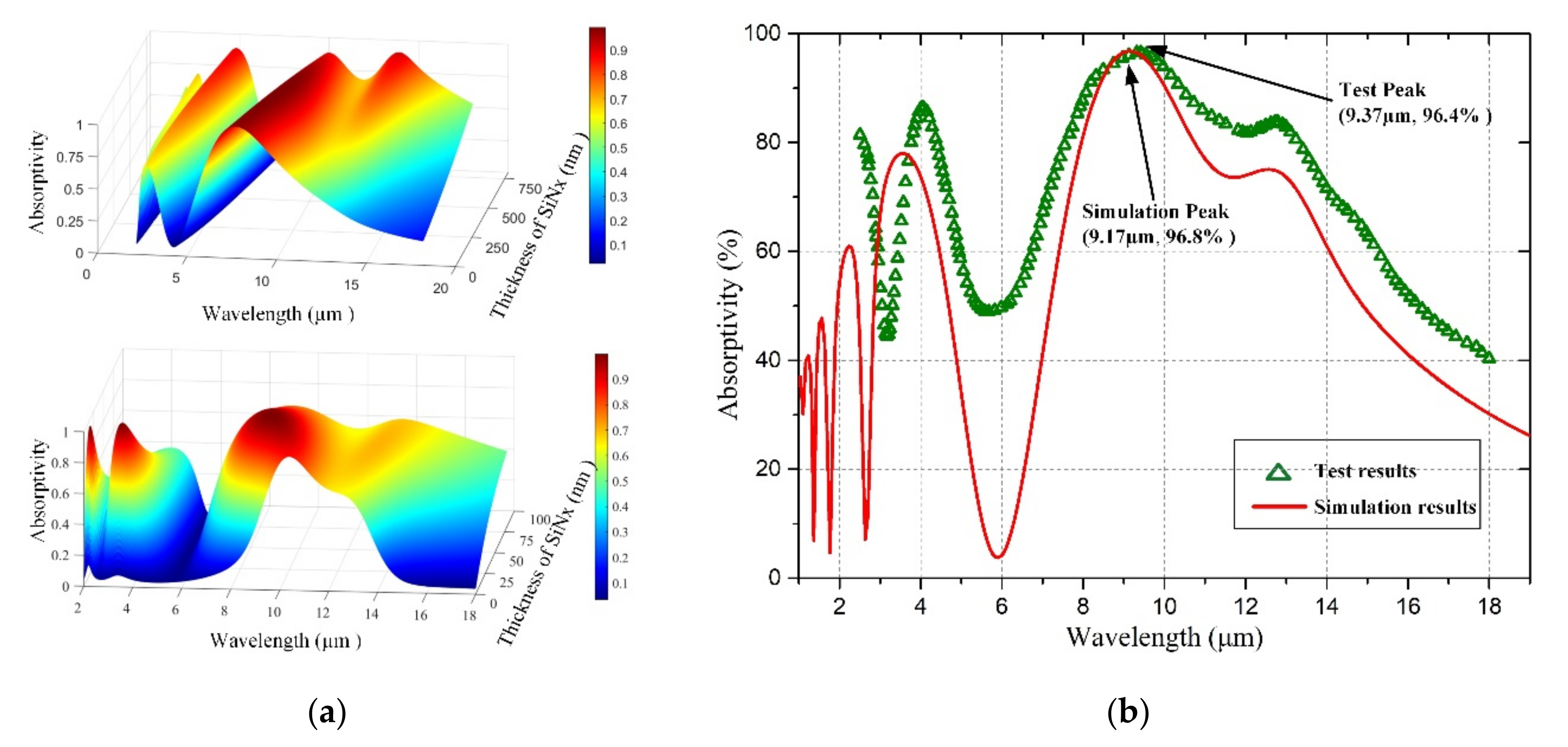
2.2. The Infrared-Absorption Structure Design

As shown in Figure 2, the micro-bolometer pixel consists of four function-based layers: (a) the molybdenum silicide infrared-absorption film, (b) the SiGe/Si multi-quantum-well thermistor layer, (c) the silicon nitride structure layer, (d) the aluminum infrared reflection layer. These layers formed a Fabry–Perot resonant optical cavity to absorb the incident infrared radiation, resulting in a temperature change in the resonant optical cavity. These temperature changes were detected by the SiGe/Si multi-quantum-well thermistor, and the changes were converted into an electrical signal by the read-out circuits. Then, the image of the incident infrared radiation was obtained by processing the read-out electrical signal. The performance of the micro-bolometer was greatly affected by the infrared absorptivity of the resonant optical cavity, which was within the specified wavelength.
Based on the optical thin-film theory, an optical matrix for the multi-layer film system is defined (shown in Equation (2)) for the resonant optical cavity [16,17]
B C = j = 1 k cos δ j η j 1 sin δ j i η j sin δ j cos δ j 1 η j + 1 ,
where [B C] T is the characteristic matrix for the multi-layer film system, k is the number of layers in the system, ηj is the optical admittance of film layer j, and ηj+1 is the optical admittance of the next layer. Here, only the normal incidence of infrared radiation is considered. Moreover, the phase thickness δj of layer j can be calculated by:
δ j = 2 π λ η j d j .
Here, λ is the wavelength of the incident radiation, dj is the film thickness of layer j. The p-like and s-like of the film’s optical admittance ηj is defined as
η j p = n j / cos θ j ,
η j s = n j × cos θ j .
where nj is the complex refractive index of layer j; θj is the infrared radiation incident angle of layer j. The transmissivity T and reflectivity R of the multi-layer film system can be derived as:
T = 4 η 0 η j + 1 ( η 0 B + C ) ( η 0 B + C ) ,
T = 4 η 0 η j + 1 ( η 0 B + C ) ( η 0 B + C ) .
Here, η0 is the optical admittance of the vacuum. In summary, the absorption ratio A of the resonant optical cavity can be calculated as follows:
A = 1 T R .
In the application, the infrared radiation in the atmosphere has a high-transmittance window at the wavelength of 8–14 µm. To achieve a better performance, the resonant optical cavity is optimized to obtain a high absorption efficiency within the working wavelength range.
According to the film’s optical parameters, applied in Table 2, the infrared-absorption surface plot of the resonant optical cavity was obtained by the MATLAB simulation [18,19]. The dependence of the resonant optical cavity on the normal incident infrared wavelength and critical layer thickness is shown in Figure 3a. Considering the fabrication error, the infrared-absorption structure is designed with an average absorption efficiency of 90%, in a wavelength of 8–14 µm. The optimized thickness range of the MoSi2 infrared-absorption layer is 15–35 nm; the optimized thickness range of the SiNx structure layer is 300–400 nm. The test structure of the resonant optical cavity is fabricated to test the infrared absorptivity of the micro-bolometer. The respective layer thickness of the test structure is shown in Table 2.
The infrared-absorption simulation of the test structure is shown as the solid red line in Figure 3b. The test result of the infrared absorption is shown as triangular datapoints in Figure 3b. The average absorption efficiency of the test structure achieves more than 90% at the wavelength of 8–14 µm. The measured result is consistent with the calculated result, and the measured result has a higher average absorption efficiency within the working wavelength range.

2.3. The Bolometer Pixel Thermal Bridge Analysis

The micro-bolometer pixel absorbs the infrared radiation, and the infrared-absorption structure is heated by these incident infrared radiations. The temperature will rise following the infrared-absorption structure of the micro-bolometer pixel and is finally transmitted to the substrate through the cantilever and Au pillar. The performance of the micro-bolometer is greatly affected by the parameters of the pixel thermal bridge.
The temperature field changes in a micro-bolometer pixel can be characterized by the heat balance Equation (9) [20]:
C d T d t = Q G T T s .
Here, Ts is the initial temperature (substrate temperature), Q is the heat input, C is the thermal capacity of the pixel, and G is the thermal conductivity of the pixel.
The thermal conductivity G of the pixel can be derived as
G = G l e g + G r a d i a t i o n + G g a s + G c o n v e c t i o n .
where Gleg is the thermal conductivity of the cantilever, Gradiation is the thermal conductivity caused by thermal radiation, Ggas is the thermal conductivity of the atmosphere, and Gconvection is the thermal conductivity caused by thermal convection. Ggas can be calculated by [21]:
G g a s = β p i x e l A p i x e l / d λ g a s 1 + γ g a s p d 1 .
Here, βpixel is the fill factor of the micro-bolometer, Apixel is the micro-bolometer pixel area (pixel pitch), p is the gas pressure, d is the distance between the infrared-absorption structure and the substrate (about 3 μm), λgas is the pressure-independent thermal conductivity of the gas in the high-pressure regime (λa = 0.024 W/K·m for standard atmospheric pressure), and γgas is the thermal conductivity per unit pressure and length in the low-pressure regime (γa = 1.9 m/K·s for standard atmospheric pressure). Under vacuum and room temperature, the thermal conductivity of cantilever Gleg is several orders of magnitude greater than other thermal conductivities (Ggas + Gconvection + Gconvection) of a micro-bolometer pixel. The thermal conductivity of cantilever Gleg can be calculated by
G l e g = λ l e g m A l e g m / l l e g .
where λleg-m is the thermal conductivity coefficient of the cantilever material, Aleg-m is the cross-section area of the cantilever, and lleg is the length of the cantilever. The thermal conductivity of the micro-bolometer pixel calculation is shown in Table 3. The total thermal conductivity of the micro-bolometer pixel is approximately 1.64 × 10⁻⁷ W/K.
The thermal capacity Cp of the pixel can be defined as:
C p = V 1 ρ 1 c 1 + V 2 ρ 2 c 2 + . .
Here, Vx is the volume of layer x, ρx is the density of layer x, and cx is the specific thermal capacity of layer x. The micro-bolometer pixel thermal capacity calculation is shown in Table 4. The total thermal capacity of the micro-bolometer pixel is approximately 1.2574 × 10⁻¹⁹ J/K.
The thermal response time of the micro-bolometer pixel is determined by the thermal capacity of the pixel and the thermal conductivity between the infrared-absorption structure and substrate. The thermal time constant τp of the pixel can be calculated by [21]:
τ p = C p / G .
With the thermal capacity of 1.2574 × 10⁻⁹ J/K and thermal conductivity of 1.64 × 10⁻⁷ W/K, the thermal time constant τp of the micro-bolometer pixel is 7.67 ms.

3. Results

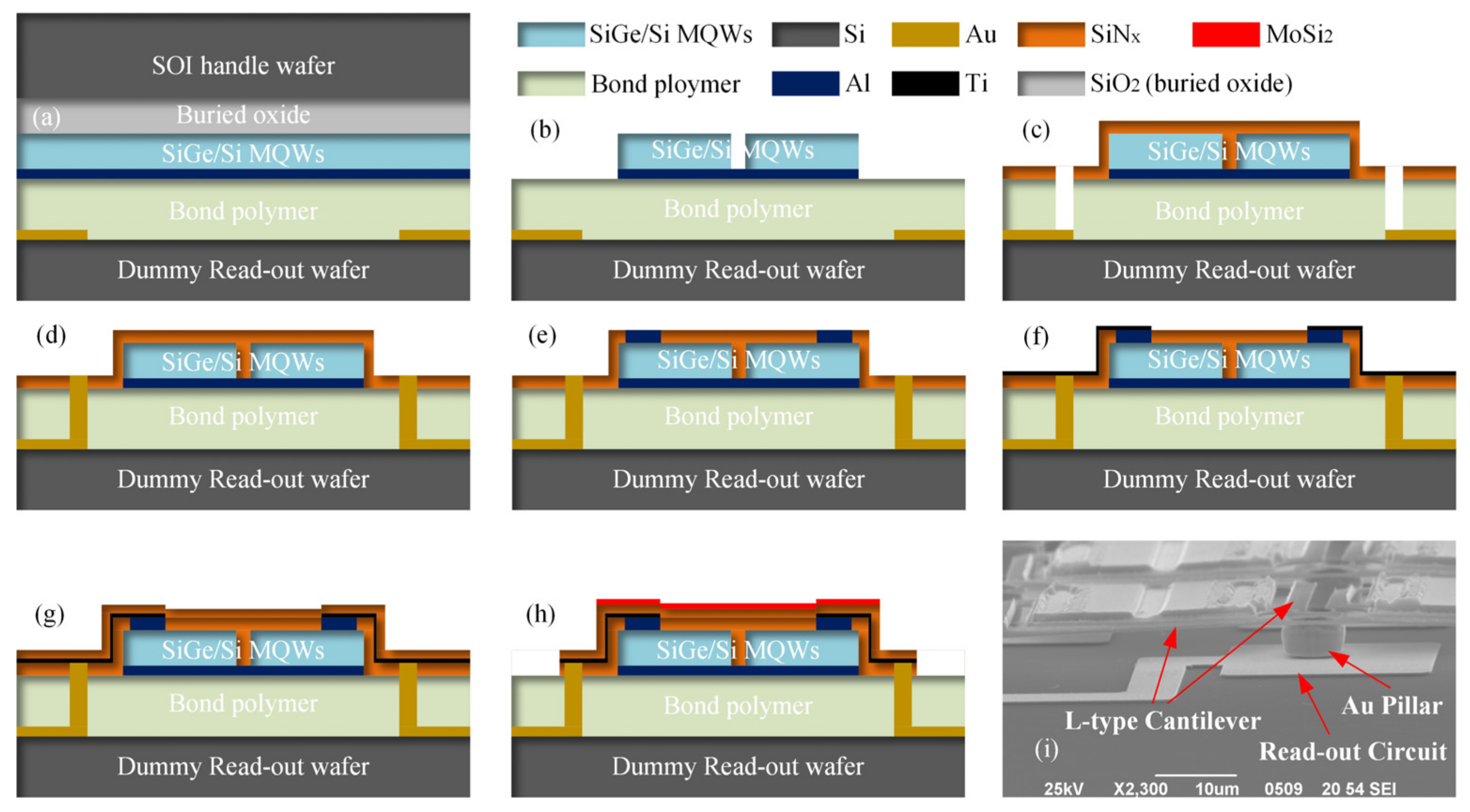
3.1. Adhesive Wafer Bonding and Micro-Bolometer Fabrication

A 100 mm SOI wafer was used as the handle wafer for the SiGe/Si MQWs epitaxial growth. The buried layer of this wafer was 1.5 µm ±10% and the SOI layer of this wafer was 180 nm ± 5%. The SiGe/Si MQWs were deposited in the reduced-pressure chemical vapor deposition (RPCVD, Epsilon 2000, ASM, Versterkerstraat, The Netherlands) reactor with the process condition of pressure 2600 Pa and a temperature of 650 centigrade. A total thickness of 370 nm monocrystalline membrane was deposited on the SOI layer (shown in Figure 4a). Considering the lattice dislocation during the epitaxial process, the Ge concentration of the SiGe layer in SiGe/Si MQWs was 30%. A 20 nm-thick Ti and 75 nm-thick Al were sputtered (LAB18, Kurt J. Lesker, Jefferson Hills, PA, USA) on top of the SiGe/Si MQWs to define the micro-bolometer pixel backside reflection layer.
The dummy read-out circuit wafer used a 100 mm Si wafer (100) as the substrate. The Au lines and Au pads of the read-out wafer were fabricated by magnetron sputtering and the lift-off process. These were used to electrically address the test pixel in the micro-bolometer arrays for characterization purposes and provided a current path during the electroplating of Au via pillars (shown in Figure 4b). The read-out wafer had a surface topography of about 300 nm, which is similar to most commercial CMOS wafers. The dummy read-out was used to replace the CMOS read-out IC wafer for fabrication experiments.
Both the SiGe/Si MQWs wafer and read-out wafer were spin-coated at 1500 rpm for 30 s with the adhesive-bonding polymer layers (mr-I 9100 m, Micro-resist Technology, BerlinGER). After that, the wafers were soft-baked at 100 centigrade for 15 min to remove the solvent and polymer pre-curing. The thickness of each adhesive-bonding polymer layer was about 1400 nm, and the total thickness of the polymer layer was about 2800 nm. The bonding defects caused by particles and topography were reduced at this thickness. Then, the wafers were heterogeneously integrated using back-alignment adhesive wafer bonding (BA6/CB-6L, SUSS Micro-Tec, Garching, GER). Figure 4c was the ultrasonic micrograph of the heterogeneous integration wafer. Several bonding defects caused by particles and three unbonded areas caused by three bonder spacers were found. The test was operated in a public laboratory, and the heterogeneous integration yield will have a higher estimate in Fab.
The Si handle layer of the SiGe/Si MQWs wafer (shown in Figure 5a) was removed by the SF6-based inductively coupled plasma (ICP) etching (MPX HRM System, STS, Wells, UK and self-stopped at the buried oxide layer. The buried oxide was removed by the buffered HF (10:1) and stopped at the SOI layer. As shown in Figure 5b, the SiGe/Si MQWs layer was patterned by lithography (MA6/BA6, SUSS Micro-Tec, Garching, GER) and CF4-based reaction ion etch (RIE, Tegal 903e, Tegal, Petaluma, CA, USA), while the Al reflection layer was etched by Ar-based ion beam etch (IBE, IBE-A-150, BCT, Beijing, PRC). Then, the first SiNx layer, 200 nm thick, was deposited by plasma-enhanced vapor deposition (PECVD, Plasmalab System 100, OxFord Instrument, Oxford, UK) with the process conditions of a pressure of 230 Pa and temperature of 200 degrees centigrade.
Figure 5c shows that the via-holes through the SiNx layer and polymer layer were etched by RIE (Plasmalab System 80, OxFord Instrument, Oxford, UK). The Au pillars were constructed by electroplating to fill the via-holes (shown in Figure 5d). Then, the Al contact pads were defined with lithography and lift-off processes (shown in Figure 5e). A 50 nm-thick Ti layer was deposited and patterned by magnetron sputtering and IBE etching. The second SiNx layer of 175 nm and the MoSi2 layer of about 20 nm were deposited, as shown in Figure 5g,h). After that, the cantilevers and the infrared-absorption structure were defined by lithography and the dry-etching process (shown in Figure 5h). Finally, the polymer layer was completely removed by isotropic oxygen plasma etching (shown in Figure 5i), and the contact resistances between the Si and Al layers were decreased by annealing in an Ar atmosphere.

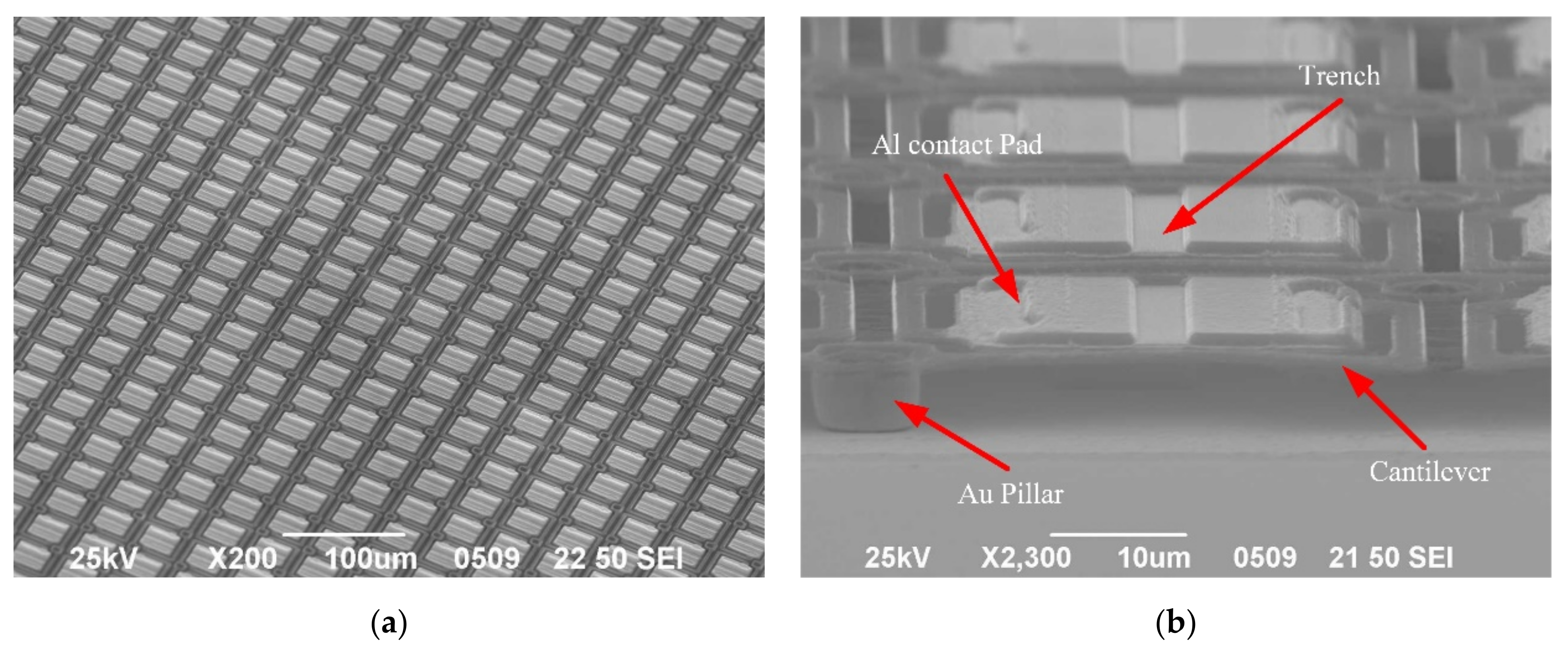
3.2. Structural Characterization of Micro-Bolometer Array

The structures after the fabrication processes are indicated in Figure 6. Each micro-bolometer die consisted of several test pixels and 320 × 240 pixels of a 40 × 40 µm pitch (shown in Figure 6a). A pixel constituted two Au pillars, two L-type cantilevers, and one infrared-absorption structure (shown in Figure 6a). The L-type cantilevers supported the pixel freestanding on the substrate, while the thermal infrared-absorption structure only supported conductive coupling to the substrate through the cantilevers and Au pillars in a vacuum. The electrical path of the pixel was connected to the Au pillars, while Ti connected the layer of the cantilevers, Al contact pads, SiGe/Si MQWs thermistor, and the Al reflection layer. The electrical connection structure of the pixel was intact. A 100 mm wafer had 30 micro-bolometer dies. Dies with a pixel-integrity ratio of more than 95% accounted for more than 70% of the total through the structural characterizations and statistics.

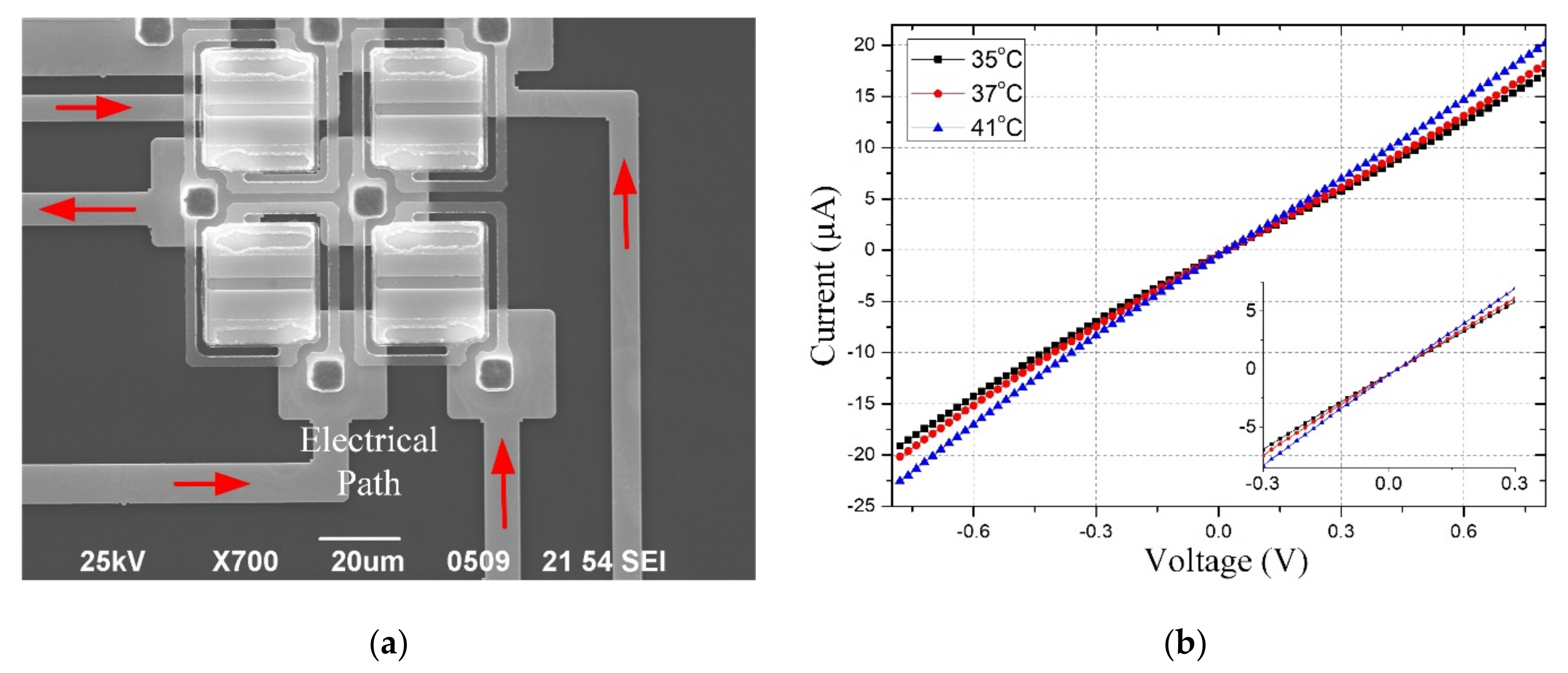
3.3. Electrical Characterization of Micro-Bolometer Pixel

The micro-bolometer die was packaged in a metal shell. Au wires connected the die electrodes and the pads of the shell. Each micro-bolometer die had several test pixels, where the die electrodes and the Au pillars of the test pixels connected via a read-out circuit. The electrical path of the test pixels is shown in Figure 7a. The I-V curves with different temperatures are shown in Figure 7b. The TCR of the test pixels can be calculated as [22]:
T C R = 2 × R 2 R 1 R 2 + R 1 × T 2 T 1 .
where R1 is the resistance of test pixels at temperature T1, and R2 is the resistance of test pixels at temperature T2.
The average TCR of pixels was approximately 2.62%/K, with an applied voltage ±0.8 V. When the applied voltage decreased to ±0.3 V, the average TCR of pixels was increased to about 2.91%/K.
A thermal response-measured system was built to evaluate the performance of the test pixels. The measuring system was formed by a vacuum pump, Wheatstone bridge, and data acquisition board (NIUSB-6366, National Instruments, Austin, TA, USA). During the test, the vacuum pump was used to ensure that the pressure in the metal shell was less than 1.3 Pa. Then, the bias voltage of 0.3 V square pulses was applied to the Wheatstone bridge, and the data acquisition board collected the responding voltage data (shown in Figure 8). According to Equation (9), the relation between the thermal time constant τp and thermal steady-state time τ0 can be derived as [22]:
τ p τ 0 = 1 e 1 1 0.63 .
As shown in Figure 8, the thermal time constant of the test pixel is 7.25 ms. The thermal conductivity G of the test pixel can be calculated by [22,23]
G = I × V 0 × T C R × R s R 0 .
Where I is the bias current, V0 is the thermal steady-state voltage, Rs is the resistance of the pixel at the start point, and R0 is the resistance of the pixel at the thermal steady state. The thermal conductivity of the test pixel was 1.645 × 10⁻⁷ W/K, according to calculations. According to Equation (13), the thermal capacity of the test pixel was 1.043 × 10⁻⁹ J/K.

4. Discussion and Conclusions

This paper presents a SiGe/Si MQWs micro-bolometer array designed and fabricated based on heterogeneous integration. The SiGe/Si MQWs materials were analyzed and deposited. The infrared-absorption structure and the thermal bridge of the micro-bolometer were calculated and designed. The infrared-absorption structure was designed with an average absorption efficiency of 90% in the wavelength range of 8–14 µm. The micro-bolometer pixel was designed with a thermal capacity of 1.2574 × 10⁻⁹ J/K, a thermal conductivity of 1.64 × 10⁻⁷ W/K, and a thermal time constant of 7.67 ms.
Based on adhesive wafer bonding, a heterogeneous integration with the SiGe/Si MQWs handle wafer, and the dummy read-out circuit wafer was achieved. A 320 × 240 micro-bolometer array of 40 µm pitch L-type pixels was fabricated. The test pixel was measured with a thermal capacity of 1.043 × 10⁻⁹ J/K, a thermal conductivity of 1.645 × 10⁻⁷ W/K, and a thermal time constant of 7.25 ms. The infrared absorption of the micro-bolometer was measured with an average absorption efficiency of 90% in the wavelength range of 8–14 µm. This proves the effectiveness of the micro-bolometer structural design. The total TCR value of the text pixel was measured as 2.91%/K, with a bias voltage of 0.3 V, which is significantly higher than traditional materials. The SiGe/Si MQWs micro-bolometer can be widely applied in commercial fields, especially in early medical diagnosis and biological detection, with continuous improvements in its performance and fabrication efficiency.

Author Contributions

Conceptualization, Z.F. and Y.H.; formal analysis, Z.F., Z.C. and Y.S.; investigation, Z.C. and J.J.; supervision, Y.H.; Writing—original draft, Z.F.; writing—review and editing, Z.F. and X.P. All authors have read and agreed to the published version of the manuscript.

Funding

This research was funded by National Natural Science Foundation (51375244, 11504173, 11502118 and 62001223), China.

Conflicts of Interest

The authors declare no conflict of interest.

References

  1. Kimata, M. Uncooled infrared focal plane arrays. IEEJ Trans. Electr. Electron. Eng. 2018, 13, 4–12. [Google Scholar] [CrossRef] [Green Version]
  2. Strojnik, M.; D’Acunto, M.; Rogalski, A. Advanced Infrared Technology and Applications 2020: Introduction to the feature issue. Appl. Opt. 2020, 59, AIT1–AIT6. [Google Scholar] [CrossRef] [PubMed]
  3. Rogalski, A.; Kopytko, M.; Martyniuk, P. 2D material infrared and terahertz detectors: Status and outlook. Opto-Electron. Rev. 2020, 28, 107–154. [Google Scholar]
  4. Wissmar, S.G.E.; Radamsson, H.H.; Yamamoto, Y.; Tillack, B.; Vieider, C.; Andersson, J.Y. SiGe quantum wells for uncooled long wavelength infra-red radiation (LWIR) sensors. J. Phys. Conf. Ser. 2008, 100, 042029. [Google Scholar] [CrossRef] [Green Version]
  5. Andersson, J.Y.; Ericsson, P.; Radamson, H.H.; Wissmar, S.G.E.; Kolahdouz, M. SiGe/Si quantum structures as a thermistor material for low cost IR microbolometer focal plane arrays. Solid-State Electron. 2011, 60, 100–104. [Google Scholar] [CrossRef]
  6. Kaynak, C.B.; Yamamoto, Y.; Göritz, A.; Korndörfer, F.; Zaumseil, P.; Kulse, P.; Schulz, K.; Wietstruck, M.; Shafique, A.; Gurbuz, Y.; et al. High performance thermistor based on Si1−x Gex/Si multi quantum wells. IEEE Electron Device Lett. 2018, 39, 753–756. [Google Scholar] [CrossRef]
  7. Kolahdouz, M.; Ostling, M.; Radamson, H.H. A low cost multi quantum SiGe/Si/Schottky structure for high performance IR detectors. In Proceedings of the European Solid-State Device Research Conference (ESSDERC), Helsinki, Finland, 12–16 September 2011; pp. 327–330. [Google Scholar]
  8. Kaynak, C.B.; Goeritz, A.; Krueger, P.; Voss, T.; Yamamot, Y.; Heinrich, P.; Saarow, U.; Wiestruck, M.; Kaynak, M. Layer transfer process development for SiGe based microbolometer integration. In Proceedings of the IEEE 8th Electronics System-Integration Technology Conference (ESTC), Tøsberg, Norway, 15–18 September 2020; pp. 1–4. [Google Scholar]
  9. Niklaus, F.; Decharat, A.; Forsberg, F.; Roxhed, N.; Lapisa, M.; Populin, M.; Stemme, G. Wafer bonding with nano-imprint resists as sacrificial adhesive for fabrication of silicon-on-integrated-circuit (SOIC) wafers in 3D integration of MEMS and ICs. Sens. Actuators A Phys. 2009, 154, 180–186. [Google Scholar] [CrossRef]
  10. Bleiker, S.J.; Dubois, V.; Schröder, S.; Stemme, G.; Niklaus, F. Adhesive wafer bonding with ultra-thin intermediate polymer layers. Sens. Actuators A Phys. 2017, 260, 16–23. [Google Scholar] [CrossRef]
  11. Forsberg, F.; Lapadatu, A.; Kittilsland, G.; Martinsen, S.; Roxhed, N.; Fischer, A.C.; Stemme, G.; Samel, B.; Ericsson, P.; Høivik, N.; et al. CMOS-integrated Si/SiGe quantum-well infrared microbolometer focal plane arrays manufactured with very large-scale heterogeneous 3-D integration. IEEE J. Sel. Top. Quantum Electron. 2015, 21, 30–40. [Google Scholar] [CrossRef] [Green Version]
  12. Wissmar, S.; Höglund, L.; Andersson, J.; Vieider, C.; Savage, S.; Ericsson, P. High signal-to-noise ratio quantum well bolometer materials. In Proceedings of the Optical Materials in Defence Systems Technology III, International Society for Optics and Photonics, Stockholm, Sweden, 29 September 2006; p. 64010N. [Google Scholar]
  13. Melnikov, M.Y.; Shashkin, A.A.; Dolgopolov, V.T.; Kravchenko, S.V.; Huang, S.H.; Liu, C.W. Effective electron mass in high-mobility SiGe/Si/SiGe quantum wells. JETP Lett. 2014, 100, 114–119. [Google Scholar] [CrossRef] [Green Version]
  14. Kuo, Y.H.; Lee, Y.K.; Ge, Y.; Ren, S.; Roth, J.E.; Kamins, T.I.; Miller, D.A.B.; Harris, J.S. Quantum-confined Stark effect in Ge/SiGe quantum wells on Si for optical modulators. IEEE J. Sel. Top. Quantum Electron. 2006, 12, 1503–1513. [Google Scholar] [CrossRef] [Green Version]
  15. Foreman, B.A. Effective-mass Hamiltonian and boundary conditions for the valence bands of semiconductor microstructures. Phys. Rev. B 1993, 48, 4964. [Google Scholar] [CrossRef] [PubMed]
  16. Parsons, A.D.; Pedder, D.J. Thin-film infrared absorber structures for advanced thermal detectors. J. Vac. Sci. Technol. A Vac. Surf. Film. 1988, 6, 1686–1689. [Google Scholar] [CrossRef]
  17. Wang, Q.; Lim, K.P. Dual-layer ultrathin film optics: I. Theory and analysis. J. Opt. 2015, 17, 035613. [Google Scholar]
  18. Mei, J.J.; Chen, H.; Shen, W.Z.; Dekkers, H.F.W. Optical properties and local bonding configurations of hydrogenated amorphous silicon nitride thin films. J. Appl. Phys. 2006, 100, 073516. [Google Scholar] [CrossRef] [Green Version]
  19. Koerner, R.; Oehme, M.; Gollhofer, M.; Schmid, M.; Kostecki, K.; Bechler, S.; Widmann, D.; Kasper, E.; Schulze, J. Electrically pumped lasing from Ge Fabry-Perot resonators on Si. Opt. Express 2015, 23, 14815–14822. [Google Scholar] [CrossRef] [PubMed]
  20. Langer, H.; Steinbicker, A.; Meister, H.; Zauner, C. Integrated thermal FE analyses and testing of prototype components for the ITER bolometer diagnostic. Fusion Eng. Des. 2015, 96, 821–825. [Google Scholar] [CrossRef] [Green Version]
  21. Fan, L.; Khodadadi, J.M. Thermal conductivity enhancement of phase change materials for thermal energy storage: A review. Renew. Sustain. Energy Rev. 2011, 15, 24–46. [Google Scholar] [CrossRef]
  22. Niklaus, F.; Decharat, A.; Jansson, C.; Stemme, G. Performance model for uncooled infrared bolometer arrays and performance predictions of bolometers operating at atmospheric pressure. Infrared Phys. Technol. 2008, 51, 168–177. [Google Scholar] [CrossRef]
  23. Wissmar, S.G.E.; Radamsson, H.H.; Yamamoto, Y.; Tillack, B.; Vieider, C.; Andersson, J.Y. SiGe quantum well thermistor materials. Thin Solid Films 2008, 517, 337–339. [Google Scholar] [CrossRef]
Figure 1. SEM photograph of the SiGe/Si MQWs with the 30% Ge content and diagram of its energy band.
Micromachines 12 01553 g001
Figure 2. L-type SiGe/Si MQWs micro-bolometer and its infrared-absorption structure sketch.
Micromachines 12 01553 g002
Figure 3. (a) The infrared-absorption surface plot of the resonant optical cavity; (b) The infrared-absorption simulation results and test results of the resonant optical cavity test structure.
Micromachines 12 01553 g003
Figure 4. Sketch of the heterogeneous integration between SiGe/Si MQWs wafer and read-out wafer: (a) The cross-section of SiGe/Si MQWs wafer; (b) The overview of dummy read-out circuit wafer; (c) The ultrasonic micrograph of bonded wafers.
Micromachines 12 01553 g004
Figure 5. Micro-bolometer fabrication process: (a) The heterogeneous integration; (b) The SiGe/Si MQWs thermistor defined; (c) The SiNx layer deposited and the etched via-holes; (d) The Au pillar electroplate; (e) The Al contact pads that were defined; (f) The patterned Ti connect layer; (g) The deposited SiNx layer; (h) The deposited MoSi2 layer and the defined pixel; (i) The final pixel.
Micromachines 12 01553 g005
Figure 6. (a) The SEM graph of the partial micro-bolometer array; (b) The SEM graph of several L-type pixels of the micro-bolometer array.
Micromachines 12 01553 g006
Figure 7. (a) The electrical path of test pixel; (b) The I–V curves of test pixels with different temperatures.
Micromachines 12 01553 g007
Figure 8. The test pixel thermal response curve of a micro-bolometer array.
Micromachines 12 01553 g008
Table 1. The TCR calculation results of the SiGe/Si MQWs with different Ge concentrations.
Ge Content10%20%25%30%35%50%
EfEv (eV)0.0990.1520.1820.2140.2480.358
TCR (%/K)1.782.472.853.263.695.12
Table 2. The film optical parameters of the infrared-absorption structure.
Refractive Index nExtinction Coefficient κThickness (nm)
MoSi2 14.75.321
SiNx2κSiN 2375
Si 33.40510
Si0.7Ge0.3 33.58040
Al256875
1 The refractive index and extinction coefficient of MoSi2 is measured by Infrared Ellipsometer (M-2000DI, J.A. Woollam, Lincoln, Dearborn, MI, USA). 2 The doping level of the SiGe/Si MQWs is 1 × 1018 cm−3. 3 The extinction coefficient of SiNx is defined as: κSiN = 0.1 + 1.76exp {−0.5[(λ − 11.45)/1.25]2}.
Table 3. The calculation of the micro-bolometer pixel thermal conductivity.
λleg-m (W/(m·K))Aleg-m (μm2)lleg (μm)Gleg (10−8 W/K)
SiNx3.22 × 0.75568.58
Ti21.92 × 0.1567.82
Total16.40
Table 4. The calculation of the micro-bolometer pixel thermal conductivity.
Thickness (nm)Vx (μm3)ρx (kg/m3)cx (W/(m·K))Capacity (10−9 J/K)
SiNx375270.734407100.6612
Si18078.4123297130.1302
Doped Si14079.723297130.1323
Si0.7Ge0.34022.83331578.60.0439
Doped Si190108.123297130.1795
Al7546.427028800.1103
Total1.2574
Publisher’s Note: MDPI stays neutral with regard to jurisdictional claims in published maps and institutional affiliations.

