Article

High-Order Sliding-Mode Control Strategy for Improving Robustness of Three-Phase Interleaved Bidirectional Converter

1
School of Information Science and Engineering, Northeastern University, Shenyang 110819, China
2
State Grid Shandong Electric Power Company, Yantai 264000, China
3
China North Vehicle Research Institute, Beijing 100072, China
*
Author to whom correspondence should be addressed.
Sustainability 2023, 15(12), 9720; https://doi.org/10.3390/su15129720
Submission received: 27 May 2023 / Revised: 16 June 2023 / Accepted: 17 June 2023 / Published: 18 June 2023

Abstract

:
In response to the era background of “comprehensive electrification” and “dual carbon plan” of electric vehicles, DC/DC converters have a good performance in terms of weight, volume, and efficiency and are widely used in fields such as solar power generation, UPS, communication, computers, and electric vehicles. At present, the DC bus voltage is an important indicator for measuring the safe and stable operation of high-voltage DC power systems in electric vehicles. Therefore, regulating the stability of bus voltage through converters has good economic benefits for the sustainable development of electric vehicles in terms of maintenance costs and effective energy management. In order to solve the problem of bus voltage resonance instability caused by negative impedance characteristics of constant power load in an electric vehicle DC power system, a sliding-mode control design strategy of three-phase interleaved bidirectional converter under constant power load was proposed. Firstly, a GPI observer was designed to estimate the state and concentrated disturbances of the system. Then, the estimated value was introduced into the controller for feedforward compensation, thereby achieving fast-tracking of the output voltage to the reference voltage. Finally, the simulation results show that the controller can effectively maintain the influence of disturbances and better improve tracking characteristics and robustness to disturbances and uncertainties.

1. Introduction

With the research boom of renewable DC power sources, research on DC microgrids is gradually expanding. Because of the obvious advantages of DC microgrid technology, its application in the field of vehicle power system is becoming more and more extensive. In the DC microgrid of electric vehicles, converters are often used to realize voltage conversion between the DC bus and load. For DC power systems, maintaining the stability of the DC bus voltage is the foundation for ensuring the stable operation of vehicles. The application of a large number of power conversion devices subject to strict closed-loop control leads to an increase in the proportion of constant power loads in the system, which greatly reduces the stability of the system when the power of such loads fluctuates [1]. The research shows that the constant power load always exhibits negative-impedance characteristics and brings an instability effect to the system. The negative-impedance characteristics of a constant power load can cause significant voltage oscillations in the system when there are significant changes in the CPL (constant power load), thereby reducing power quality and posing safety hazards [2,3].
Therefore, how to keep the DC bus voltage of electric vehicles quickly adjusted and stable is the key problem with the DC microgrid. The DC microgrid of electric vehicles is a system composed of many parts, its instability phenomena are various, and the mechanism of the system instability is also complicated. Since most distributed power generations, energy storage devices, and loads in the DC microgrid need to be connected with the DC bus through converters, and these power electronic converter devices have nonlinear characteristics, the power electronic system composed by them also has nonlinear characteristics [4].
In practical applications, the system model will be affected by various disturbances, such as the uncertainty of inductance and magnetic characteristics, the instability of input voltage, the disturbance of load, etc. At present, many advanced nonlinear control methods have been applied to the converter, such as active disturbance rejection control, adaptive control, sliding-mode control, etc. The sliding-mode control has the advantages of simple operation, high precision, good stability, and robustness in practical applications. Sliding-mode control technology and a DC-DC converter work well together because they are both based on a variable-switching strategy [5]. For the SMC (slide-mode control) method, Reference [6] ensured large signal stability and a fast dynamic response. In order to further improve the transient dynamics of the system, a simple finite-time convergence SMC method is adopted in the converter system [7,8]. However, it is difficult to maintain high accuracy in the event of external disturbances or changes in internal components. Therefore, modern advanced control methods are studied, such as sliding-mode control, adaptive control, optimal control, predictive control, etc. The above control method basically solves the problem of output-voltage instability. However, these methods cannot quickly track and suppress interference. For closed-loop systems, it is difficult to achieve a good voltage output performance under interference.
Considering the perturbations and uncertainties existing in practical applications, it is difficult to measure them with actual sensors, but the designed observer can achieve accurate estimation and compensation of perturbations. In Reference [9], an expanded state observer was designed to realize the estimation of load changes, and a sliding-mode controller was designed to improve the anti-interference performance of the system. Reference [10] designed the unknown input observer, which has low sensitivity to noise and only needs to adjust one parameter, which is easy to implement in the actual system. Reference [11] proposed a sliding-mode control method based on the disturbance observer, which can converge to the neighborhood near the reference voltage in a finite time. However, the above observer can only accurately estimate the slow time-varying perturbations [12]. The perturbations in the actual system are more complex, and there may be higher-order polynomial perturbations. Reference [13] proposed a passive controller based on interconnection and damping allocation, which is robust and easy to implement. However, it can lead to a slow transient response.
In Reference [14], the GPI (generalized proportional integral) observer was designed to achieve an accurate estimation of slow and fast time-varying disturbances, and it was combined with the backstepping method to deal with the unmatched load disturbance. The basic idea of the backstepping method is to decompose a complex system into multiple subsystems, which are recursive from backward to forward through the design of the virtual control law. Interference factors are designed into each subsystem, but in the design process, there may be a high-order derivative of the virtual control function in the controller, which is more complicated to calculate.
In these controllers, in order to maintain the stability of the output voltage, the switch gain is required to be greater than the upper limit of the disturbance. However, in some low-order sliding-mode control laws, an excessive switching gain can lead to significant voltage fluctuations, resulting in unstable output voltage in the practical-implementation literature [15,16]. The interference estimation and compensation technology provide a feasible method to alleviate the chattering phenomenon in Reference [17]. In Reference [18], the nonlinear disturbance observer was used to estimate the uncertain power change, which provides a new way of thinking for dealing with CPL problem. It is difficult for the observer to obtain satisfactory estimation accuracy when dealing with a fast time-varying CPL. There is also no consideration of supply voltage fluctuations. Performance degradation is caused by these factors. Reference [19] proposes a distributed current-sharing control method. The outer loop is the voltage droop control with the purpose of embedding virtual impedance, while the inner loop is the PI control, which can improve the dynamic and steady-state performance of the system. References [20,21] compensated for the virtual impedance coefficient by actively detecting line impedance to achieve current equalization, and they improved the voltage drop through voltage observer feedforward compensation control. Reference [22] proposed an algorithm for compensating for a current imbalance caused by resistance mismatch. By perturbing the duty cycle of one phase and measuring the deviation of other phase duty cycles, the degree of parameter mismatch is estimated, and current balance is achieved through appropriate compensation coefficients.
There are many effective error estimation methods, including the unknown input observer (UIO) [23], disturbance observer (DOB) [24], and extended state observer (ESO) [25]. The disturbance-observer-based control (DOBC) has been proven to effectively reduce unknown external disturbances and system uncertainty. Due to the fact that these observer techniques are model based, a large amount of information needs to be considered when establishing interference observers. However, both DOB and ESO can only estimate constant and stage constant perturbations and cannot estimate polynomial perturbations.
Due to the uncertainty of converter parameters and the influence of concentrated disturbances, there is an increasing amount of research on the precise estimation of disturbances, using the estimated values as feedforward compensation to improve the anti-interference performance of control. Disturbance-observer-based control (DOBC) considers the parameter changes, load changes, and input voltage fluctuations of the filter as external disturbances to the system. The disturbance observer is used to nominal the controlled object and observe these disturbances through the disturbance observer. The observed values are then fed forward to the output of the voltage control loop to counteract the impact of disturbances on the system. Another disturbance estimation technique is the extended state observer (ESO), which treats both internal uncertainties and external disturbances as total disturbances, treats the total disturbance as a new system state, estimates the system state and disturbances through internal calculations, and then designs the controller by combining the estimated values with the improved sliding-mode control method, so that the output voltage of the converter can track the reference signal quickly [26].
In order to suppress load resistance interference and input voltage changes, an SMC method based on GPI observer for three-phase interleaved parallel DC/DC converter is proposed. Estimate the disturbance and state of the system by designing a GPI observer [27]. Then, based on the estimated values obtained from the GPI observer, a composite controller is constructed using SMC technology, which enables the output voltage to asymptotically track the reference voltage [
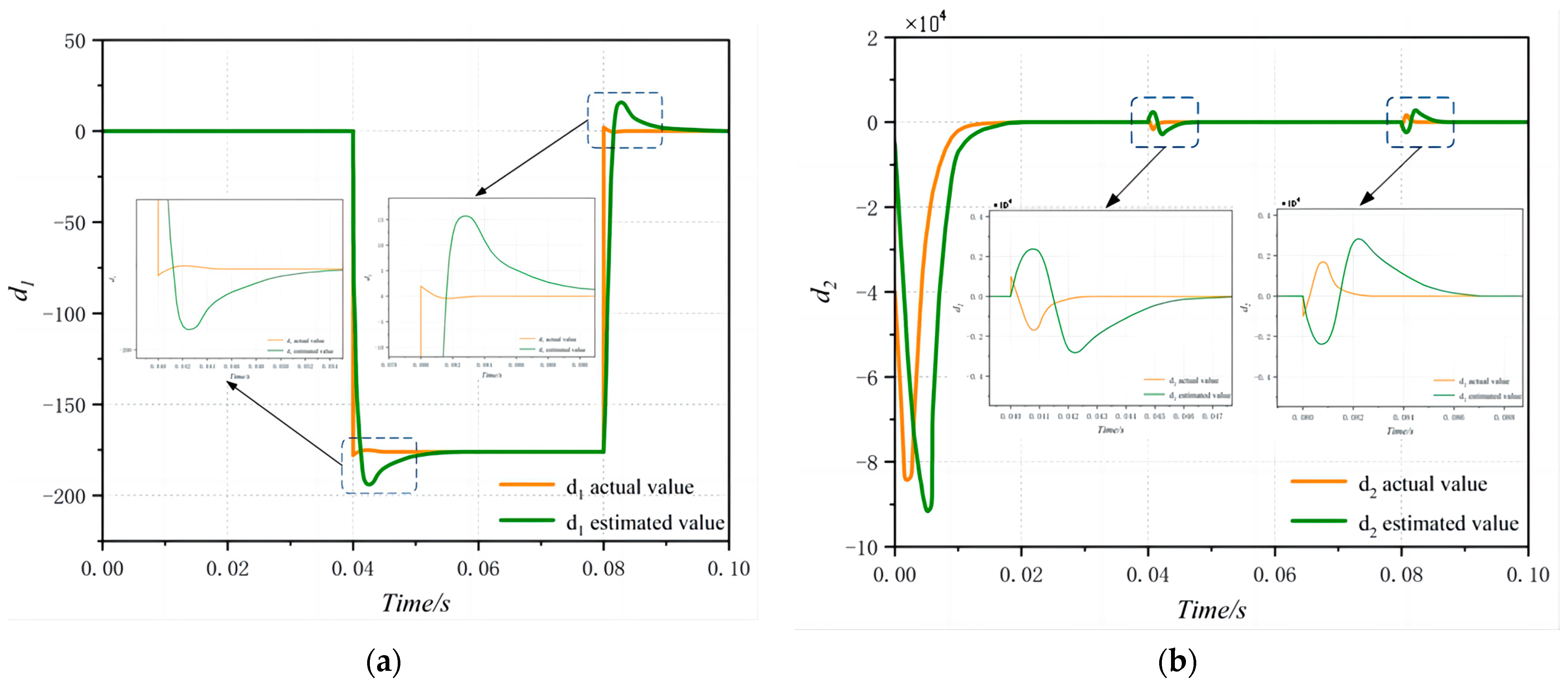
28]. The simulation results show that, compared with the sliding-mode control method based on NDO, this control method can track the reference value faster and improve the steady-state performance of the system. Meanwhile, this method reduces costs in practical systems.
The GPI observer sliding-mode control method based on the second-order sliding-mode algorithm proposed in this article can achieve small switching gain without sacrificing interference suppression by combining interference estimation, ensuring the stability of the output voltage. Compared with other observer control methods, it has strong robustness against disturbances.
The main work content of this paper is divided into three parts:
  • The stability of three-phase interleaved parallel DC/DC converter supplying CPL in electric vehicle DC power system is analyzed, and its mathematical model is established.
  • The sliding-mode control strategy based on the GPI observer can effectively reduce the switching gain by compensating the lumped disturbance accurately.
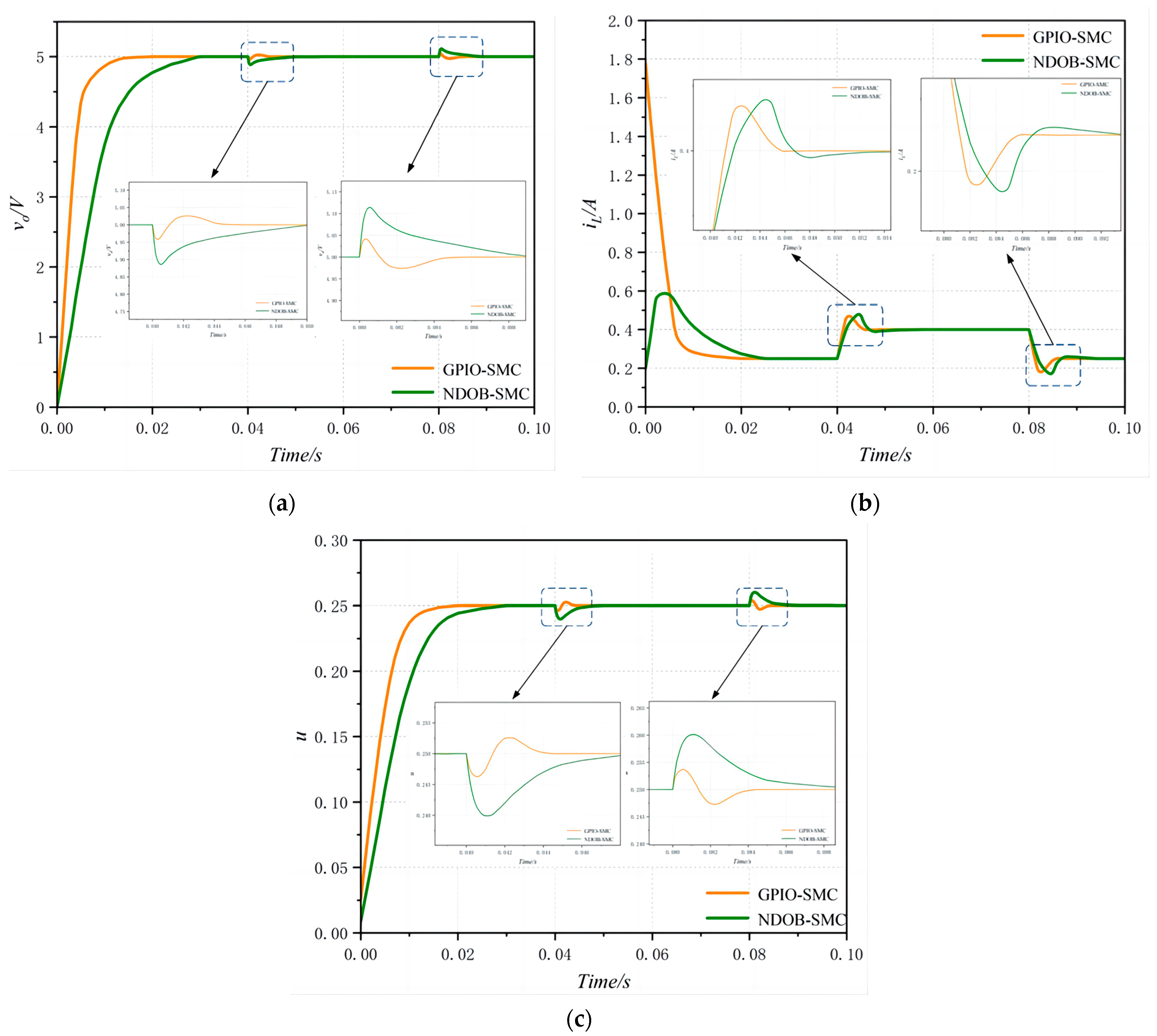
  • Through the simulation study of MATLAB/Simulink in the interference of input voltage and CPL power and the evaluation of the proposed composite controller, the correctness of the proposed controller is proved.

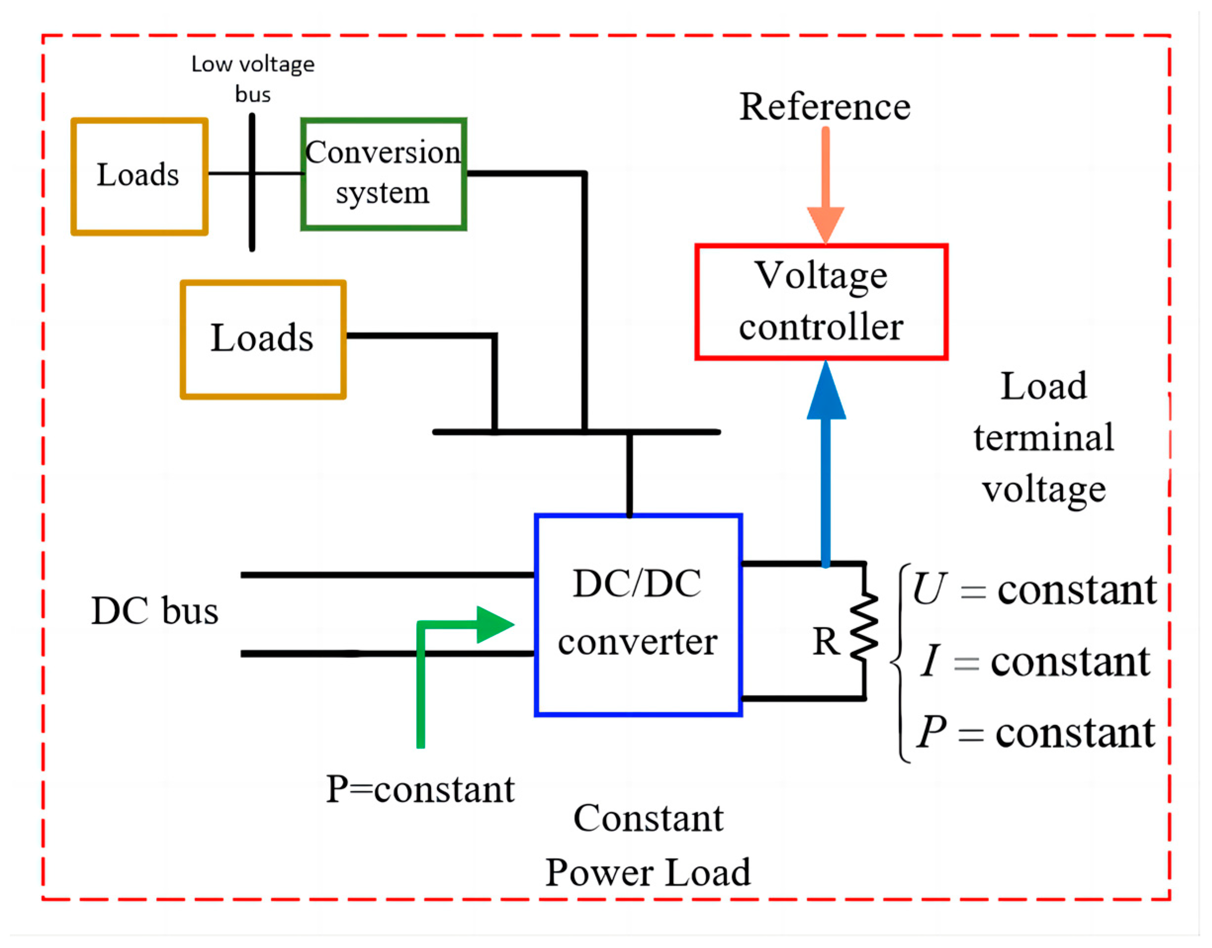
2. Stability Analysis of DC Power System for Electric Vehicles

The DC power system of electric vehicles is mainly composed of a power generation unit, generator set, energy storage unit, AC/DC load, and power converter connected to each unit module. As shown in Figure 1, in a power generation unit, the energy flows in one direction, the battery is connected to the DC bus by a DC/DC converter, and the generator set provides energy to the bus by an AC/DC converter.
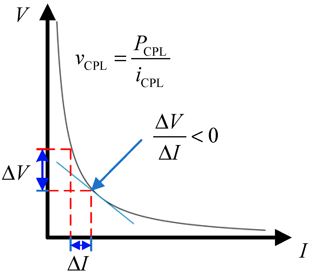
All kinds of power electronic devices in the power system of electric vehicles are connected to the on-board high-voltage power supply system of electric vehicles in the form of a cascade, and most of these power electronic devices adopt closed-loop control; when the bus voltage changes, the output power can remain constant. When the input voltage changes, the input current changes in the opposite trend; constant power load has negative impedance characteristics. It is therefore said to have a negative impedance characteristic (ΔV/ΔI < 0) constant power load.
In a constant power load, P is constant. Thus, as shown in Figure 2, as the voltage at both ends of a constant power load increases/decreases, its current decreases/increases. Because the incremental impedance of CPL is negative (ΔV/ΔI < 0), in this case, the system will deviate from its stable region, resulting in CPL negative impedance instability [29]. Interaction with other devices may affect the dynamic characteristics and stability of the system.
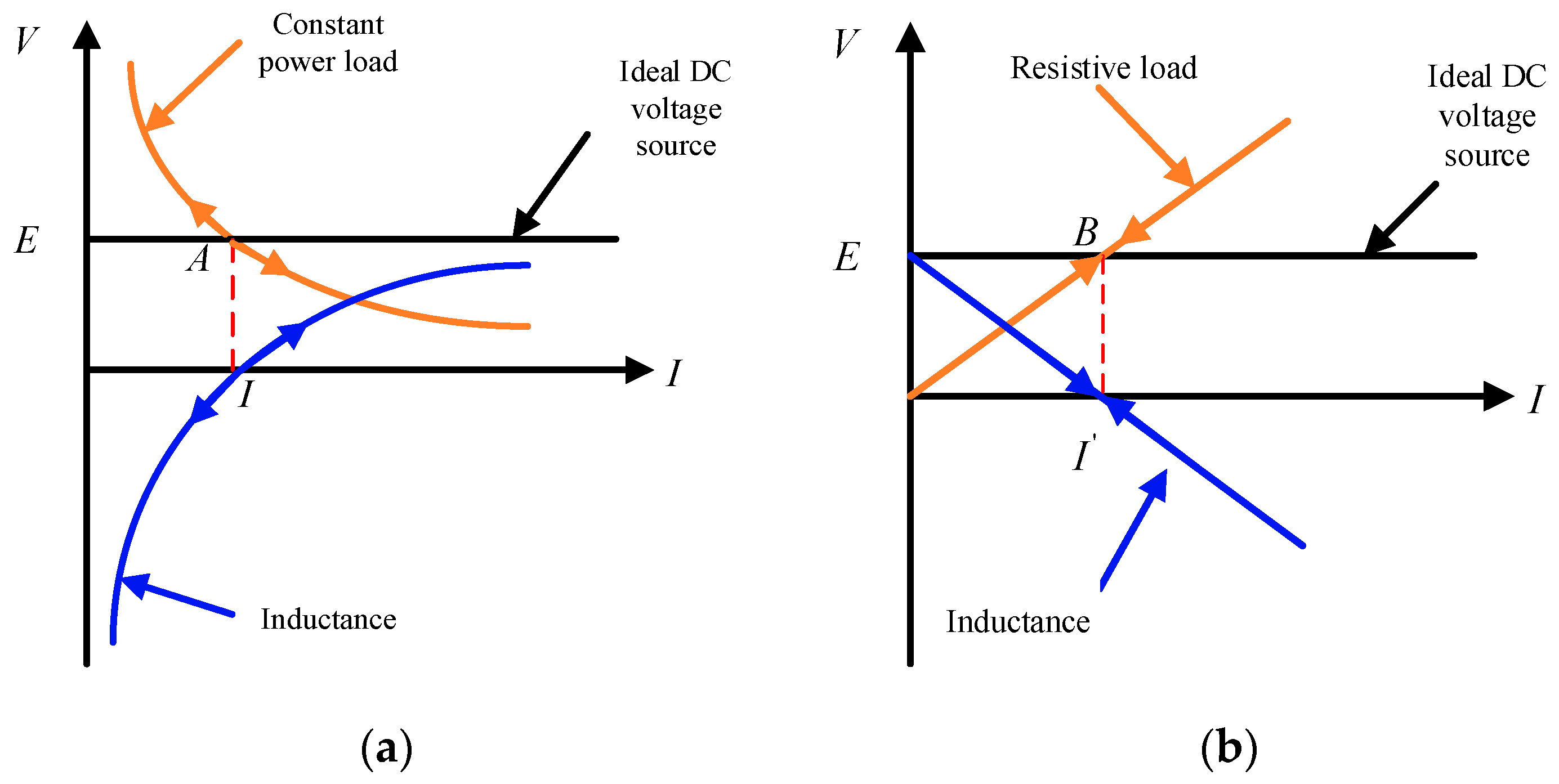
As shown in Figure 3a. The midpoint is the initial stable operating point of the system. When the system is subjected to external disturbances causing an increase in the input current of the CPL, as can be seen from Figure 3a, the voltage at both ends of the CPL is at this time, and according to KVL, the voltage at both ends of the filtering inductor is at this time. At this point, the inductance current will further increase, causing the system to move away from the stable operating point. On the contrary, when the input current of the CPL decreases due to external disturbances in the system, the voltage at both ends of the CPL is reduced. From KVL, it can be seen that the voltage at both ends of the filter inductor is reduced, and the inductor current will further decrease, thus keeping the system away from the stable operating point. The obtained volt ampere characteristic curve is shown in Figure 3b for when the load is a pure resistive load, where the point is the initial stable operating point of the system. When external disturbances increase the input current, there is a filter inductance voltage, which can be determined by KVL. At this time, the current will correspondingly decrease, so the system can return to the initial stable operating point; that is, the system is stable. CPL negative impedance was obtained via a small signal analysis [30]. In Reference [30], the equivalent model of CPL was extracted through a small signal analysis and a large signal analysis.
In order to analyze the three-phase interleaved parallel DC/DC converter system supplying CPL, the conjugated model and circuit were extracted for a small signal analysis. Based on the analysis of Reference [3], the destabilizing effect and limit of CPL negative impedance on converter were explained. Since the root of the characteristic equation is on the right-hand side, there is negative impedance instability in the output voltage of the system. In addition, the control performance is severely degraded due to the inevitable voltage fluctuations in the DC supply voltage [31].
According to the research of Reference [3], through the small signal analysis of the system equation of state, the transfer function of the system can be obtained as follows:
G s = 1 d U bus I L Ls LCs 2 + L R L s + 1 d 2 ,
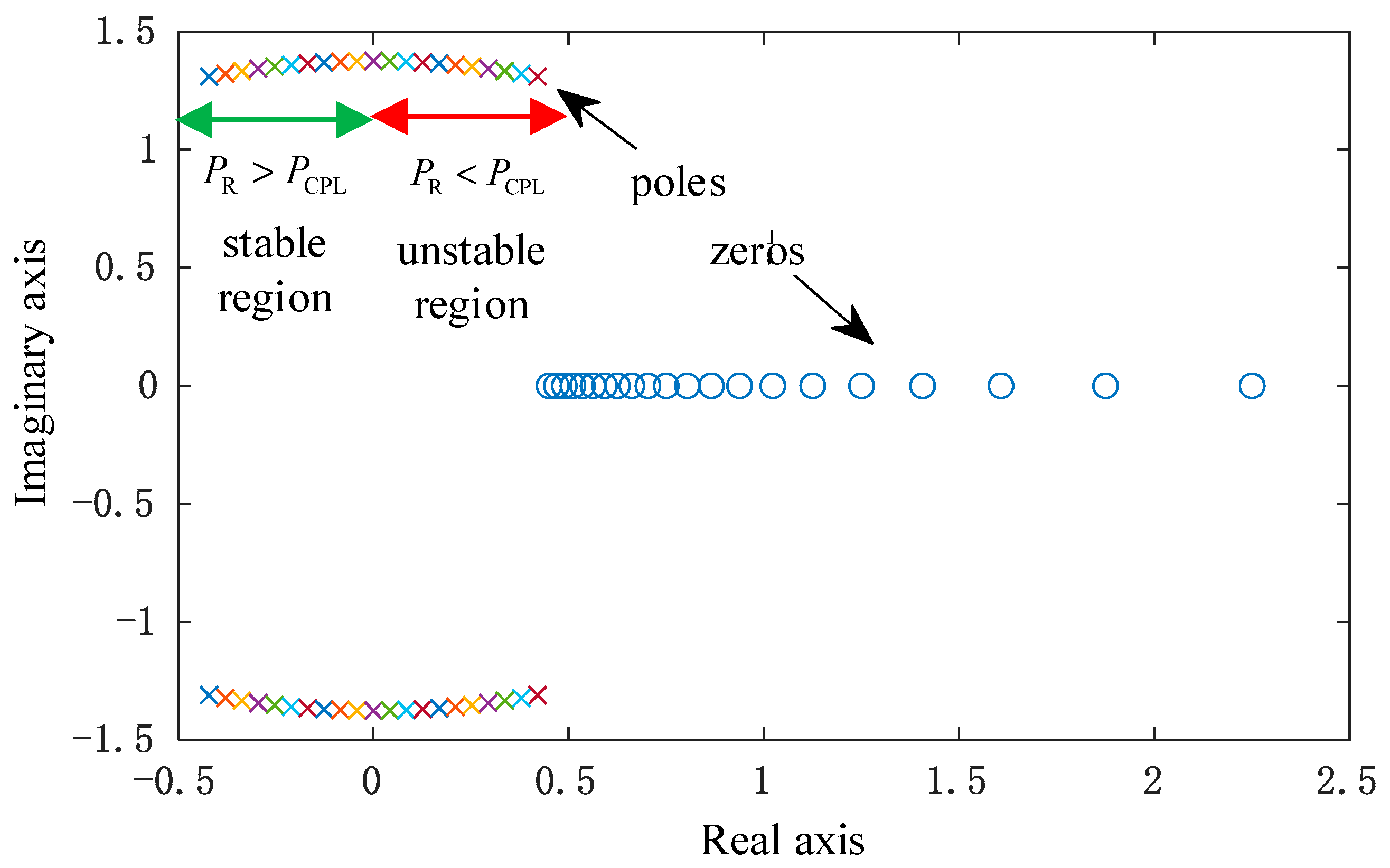
From the transfer function, with the increase of CPL power, the negative incremental resistance characteristic of CPL becomes more obvious, and the root of the system characteristic equation begins to move to the right of the complex plane. As shown in Figure 4, once the power consumed by CPL exceeds the power consumed by resistive loads, that is, P C P L > P R , CPL plays a dominant role in the system. The damping coefficient of the corresponding system is less than 0, and the slope of the output characteristic curve is negative. In this case, the DC bus voltage will be in an oscillating state. When the power consumption of CPL is less than that of resistive load, that is, P C P L < P R , the resistive load plays a dominant role in the system, the damping coefficient of the corresponding system is greater than 0, and the slope of the output characteristic curve is positive. Under this condition, the DC bus voltage of the system is in a stable state.
In order to elucidate the impact of CPL power fluctuations on the stability of the DC bus voltage, we first introduced some common CPLs in special vehicles and preliminarily analyzed the dynamic characteristics of negative incremental resistance of constant power loads. Secondly, through a theoretical analysis, we found that the power imbalance between the generating and receiving ends is the fundamental cause of bus voltage fluctuations. Then, based on small signals, the reason for the low-frequency oscillation of the DC bus caused by CPL was obtained. Through a simplified circuit analysis of an ideal voltage source, filter inductor, and CPL in series, it was found that when CPL power fluctuates, it amplifies the power fluctuation, causing the system to move away from the initial operating equilibrium point.

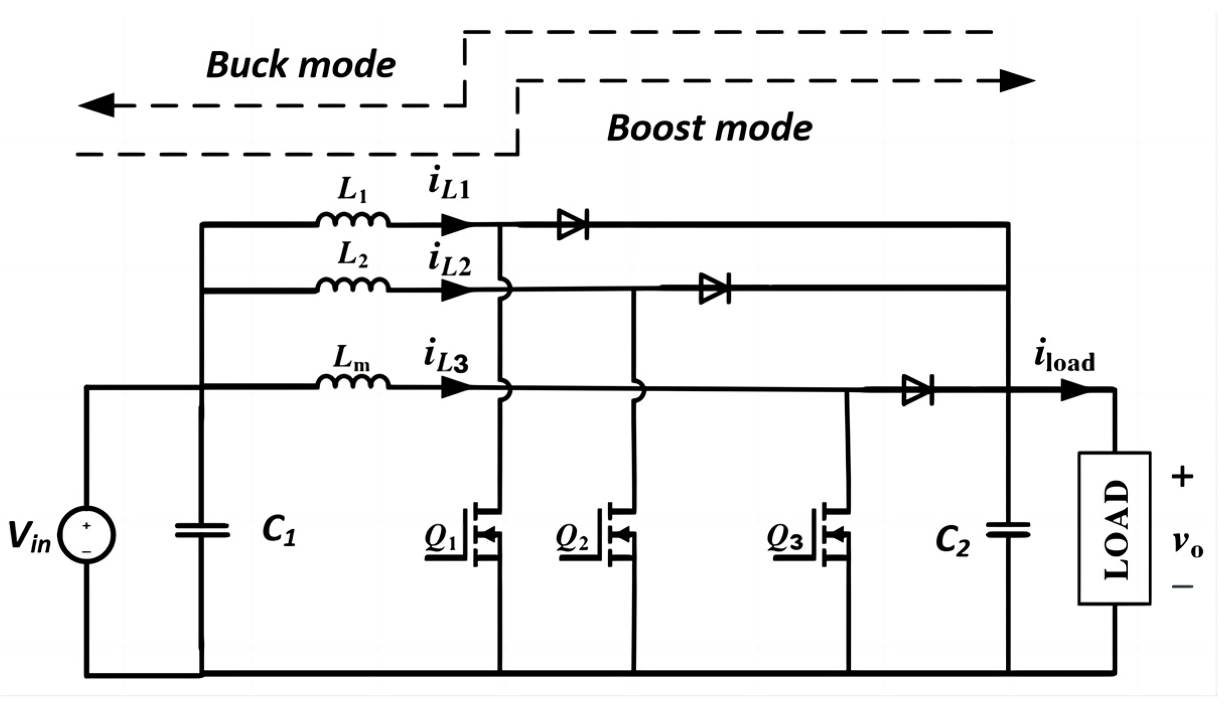
3. Modeling of Three-Phase Interleaved Parallel Bidirectional Converter

The main circuit topology of the three-phase interleaved parallel bidirectional half bridge DC-DC converter is shown in Figure 5, consisting of three bidirectional Bucks–Boosts in parallel. In the same switching cycle, only one switch tube is on the upper and lower bridge arms of the half-bridge switch tube. According to the conduction state of the switch tube, there are two states: Boost and Buck. When the energy storage capacitor releases the stored energy to the load end, the input end of the converter can be approximated as a constant voltage source, and the energy flows from the input end to the load end, where the converter is in a Boost state. When the load side needs to store energy, it operates in Buck mode, and the load-side power flows to the input side to charge the energy storage capacitor. The topology parameters of the three-phase interleaved parallel converter are shown in Table 1.
The advantages of adopting an interleaved parallel structure in bidirectional DC/DC circuits are, on the one hand, under a certain power output, the voltage and current stress of the inductor are reduced, allowing for the selection of smaller inductors, thereby reducing the volume and weight of the converter; and, on the other hand, the difference between the PWM driving waveforms of each phase is 120°, further reducing the input current ripple, reducing the inductance, while also reducing the output voltage ripple and reducing the capacitor voltage and current stress, thus ensuring that the bidirectional DC/DC converter has a higher power density. For the convenience of analysis, if the switching frequency is set to fs and the influence of voltage dead band is ignored, then ws = 2 πfs. Ts = 1/fs. 
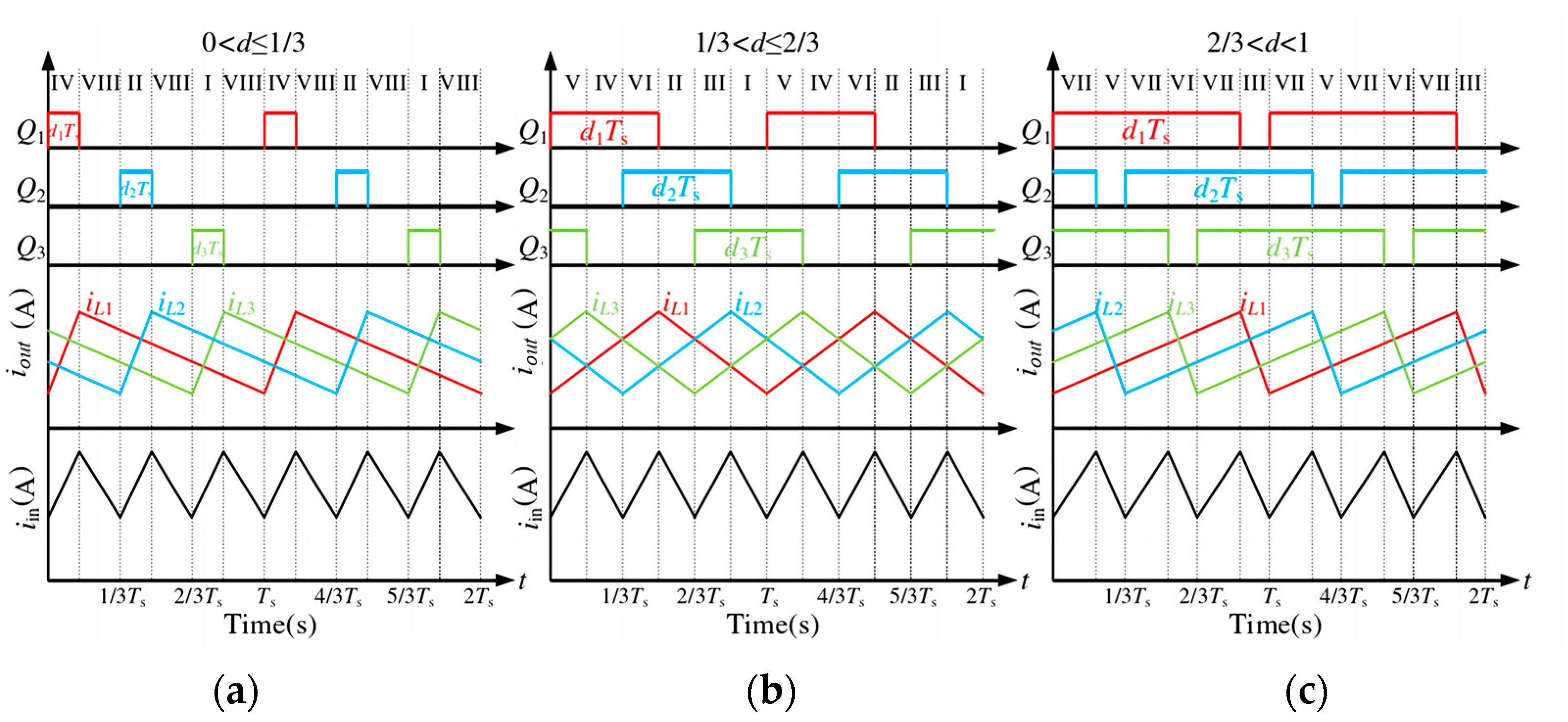
Figure 6 shows the main waveforms of the three-phase interleaved parallel boost converter under different duty ratios, d.
Assuming that the duty cycle, d, of each switch tube is equal and each phase is 120° different in sequence, there are eight switching modes of the converter. Use “1” and “0” to represent the “on” and “off” of the switch tubes, respectively. The switch states of switch tubes Q1, Q2, and Q3 can be represented as corresponding binary numbers: 001 (Mode I), 010 (Mode II), 011 (Mode III), 100 (Mode IV), 101 (Mode V), 110 (Mode VI), 111 (Mode VII), and 000 (Mode VIII). 
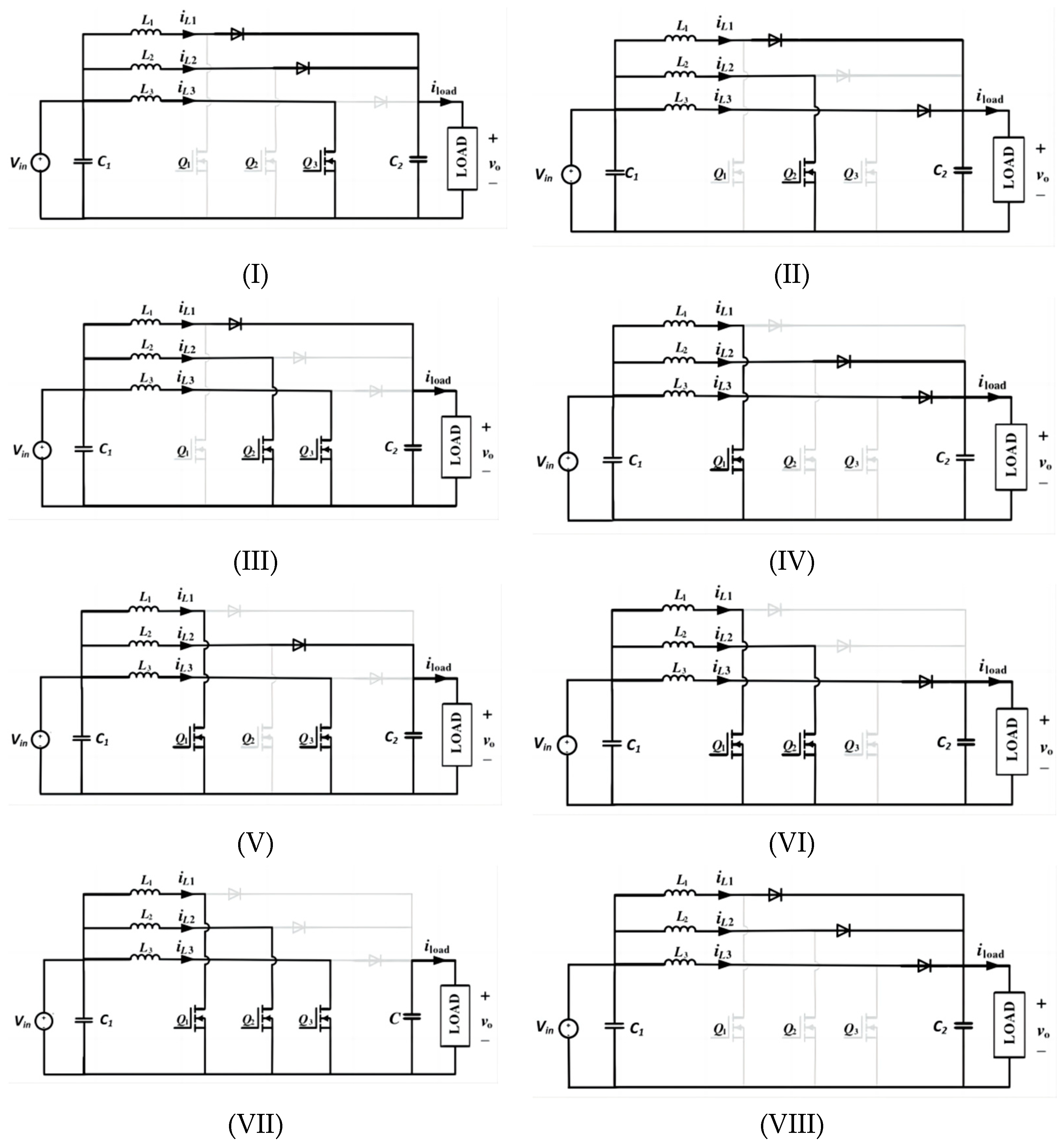
Figure 7 shows the equivalent circuits with 0, 1, 2, and 3 switch tubes on, respectively.
For the convenience of description, this article takes one of the situations as an example for analysis, while other situations can be analogized. When the duty cycle is 0 < d < 1/3, the converter can be divided into six working modes based on the power switch on/off situation. The driving signal and inductance current waveform of the corresponding switch in the system under these six working modes are shown in Figure 6a.
Process 1: (Corresponding Mode IV) The switch Q1 is in a conductive state, and the current of inductor L1 continues to increase. The vin end charges the inductor L1, Q2 and Q3 are in the off state, and the current of inductors L2 and L3 continues to decrease. Inductors L2 and L3 discharge towards the vo terminal.
Process 2: (Corresponding Mode VIII) Switch tubes Q1, Q2, and Q3 are in the off state, and the current of inductors L1, L2, and L3 continues to decrease. Inductors L1, L2, and L3 discharge towards the vo terminal.
Process 3: (Corresponding Mode II) The switch tube Q2 is in a conductive state, and the current of inductor L2 continues to increase. The vin end charges the inductor L2, Switch tubes Q1 and Q3 are in the off state, and the current of inductors L1 and L3 continuously decreases. Inductors L1 and L3 discharge towards the vo terminal.
Process 4: (Corresponding Mode VIII) Switch tubes Q1, Q2, and Q3 are in the off state, and the current of inductors L1, L2, and L3 is continuously decreasing. Inductors L1, L2, and L3 discharge towards the vo terminal.
Process 5: (Corresponding Mode I) The switch Q3 is in a conductive state, and the current of inductor L3 continues to increase. The vin end charges the inductor L3. The switch tubes Q1 and Q2 are in a conductive state, and the current of inductors L1 and L2 continues to decrease. Inductors L1 and L2 discharge towards the vo terminal.
Process 6: (Corresponding Mode VIII) Switch tubes Q1, Q2, and Q3 are in the off state, and the current of inductors L1, L2, and L3 continues to decrease. Inductors L1, L2, and L3 discharge towards the vo terminal.

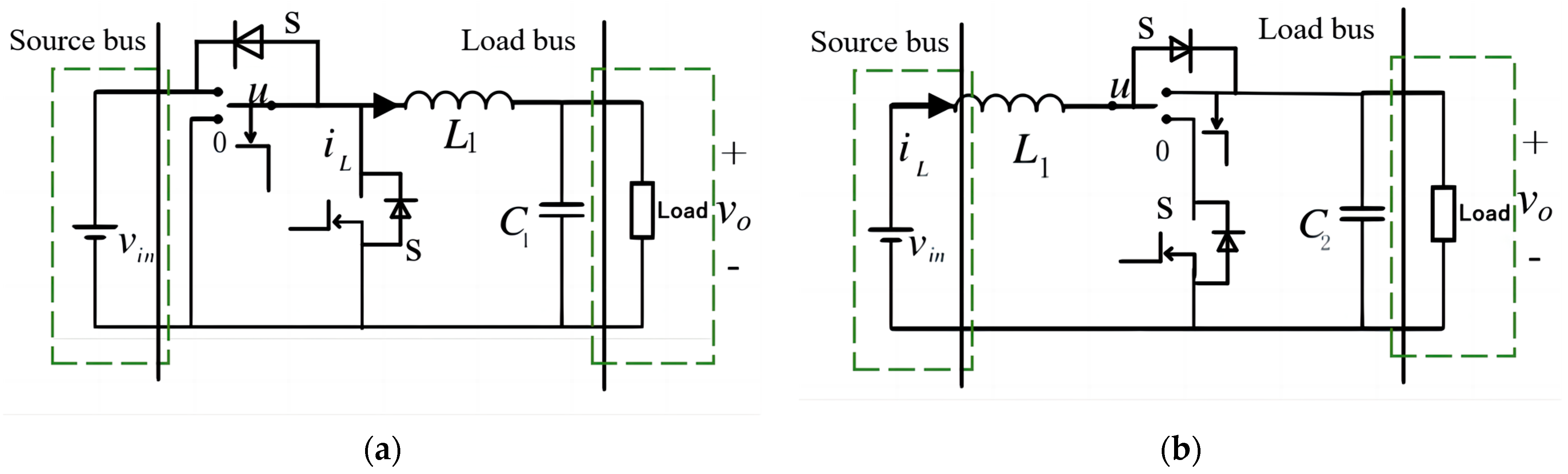
3.1. Modeling of Three-Phase Interleaved Parallel DC/DC Converter Circuit

Based on the circuit structure and working principle of a three-phase interleaved parallel bidirectional DC-DC converter, this article divides it into three identical Buck–Boost circuits, without considering the parasitic components of capacitors and inductors. The control flowchart of the composite controller is shown in Figure 8.
The equivalent circuit diagram is shown in Figure 9a for when the converter is used as a Boost converter. The equivalent circuit diagram is shown in Figure 9b for when the converter is used as a Buck converter. The topology parameters are shown in Table 2.
The results of variable structure theory analysis can be used to obtain the state equation of the bidirectional DC-DC converter in Buck mode with continuous inductance current as follows:
Firstly, the Buck circuit is modeled and studied, and its equivalent circuit topology is shown in Figure 9. Write the state equation in stages and calculate the average variable.
(1)
In 0 ≤ t ≤ d T S , switch the tube S conduction and diode VD cutoff, and, at this time, there is the following equation of state.
L di L t dt = u in t u o t C du o t dt = u o t R CPL + i L t ,
(2)
In dT S ≤ t ≤ T S , switch S off, diode VD conduction, and the inductor L release magnetic field can supply constant power load at the same time to charge the capacitor. The equation of state is as follows.
L di L t dt = u o t C du o t dt = u o t R CPL + i L t ,
By averaging (2) and (3), the following matrix equation can be obtained.
di L dt du o dt = 0 1 L 1 C 1 1 C 1 R i L u o + u in L 0 u ,
The state space equation in Boost mode with a continuous inductance current is as follows:
di L dt du o dt = 0 1 L 1 C 2 1 C 2 R i L u o +     u o L i L C 2 u + u in L 0 ,
The transfer function can be derived through Laplace transform, using the average state space equation:
G id s = v in 1 + R L Cs R L + Ls + R L CLs 2 G vd s = R 1 + R L Cs ,
This article first analyzes the Buck pattern.
P = u o 2 R L ,
where d is the duty cycle of the converter, and T is the switching cycle. A dynamic model of the Buck converter was established using the state-space averaging method. By substituting Equation (7) into (4) and linearizing it, we obtain the following:
di L dt = v in L u v o L du o dt = i L C P Cv o v o R L C ,
The voltage tracking error is defined as x 1 = e = v o v ref , where v ref is the reference voltage. The dynamic model in Equation (8) can be rewritten as follows:
x ˙ 1 = i L C v o R L C v ˙ ref + d 1 t ,
where d 1 t = P Cv o , and another state variable is defined as x 2 = i L C v o R L C , so take the derivative of that and obtain the following:
x ˙ 2 = u LC v in 0 x 1 + v ref LC x 2 R L C + d 2 t ,
where d 2 t = 1 RC d 1 t + v in v in 0 LC , d 2 t is a more complex form of time varying, consisting of a constant power load and fluctuations in input voltage. The following equation can be obtained by sorting out Equations (9) and (10):
x ˙ 1 = x 2 + d 1 x ˙ 2 = u LC v in 0 x 1 + v ref LC x 2 R L C + d 2 ,

3.2. Observer-Based Sliding-Mode Control (SMC) Design

This section’s control objective is to design a generalized proportional integral observer to estimate the time-varying disturbance and update it into the controller in real time, so as to effectively suppress the influence of the disturbance and improve the anti-jamming performance of the whole system.
Sliding-mode control uses the designed control function to make the motion state of the system in “sliding mode”, which is a discontinuous switching control, so it is also called sliding-mode variable structure control. The basic idea of the sliding-mode variable structure control theory is to consider a nonlinear system and assume that there is a phase plane, which is called the sliding-mode surface, and a point in the plane is called a balance point. Using this sliding surface as a reference path, through effective design, the state variable of the system, i.e., the controlled trajectory, is attracted to slide along the set trajectory of the reference path and converges to the equilibrium point, regardless of the initial state of the system [32,33,34].
The sliding-mode control needs to meet the following three basic conditions: existence, accessibility, and stability. Existence refers to the existence of a sliding surface in a system. Reachability refers to the ability of points outside the sliding surface of a system state to move to the sliding surface within a finite time [35,36,37,38,39]. Stability refers to the ultimate stability of the system state under model control.
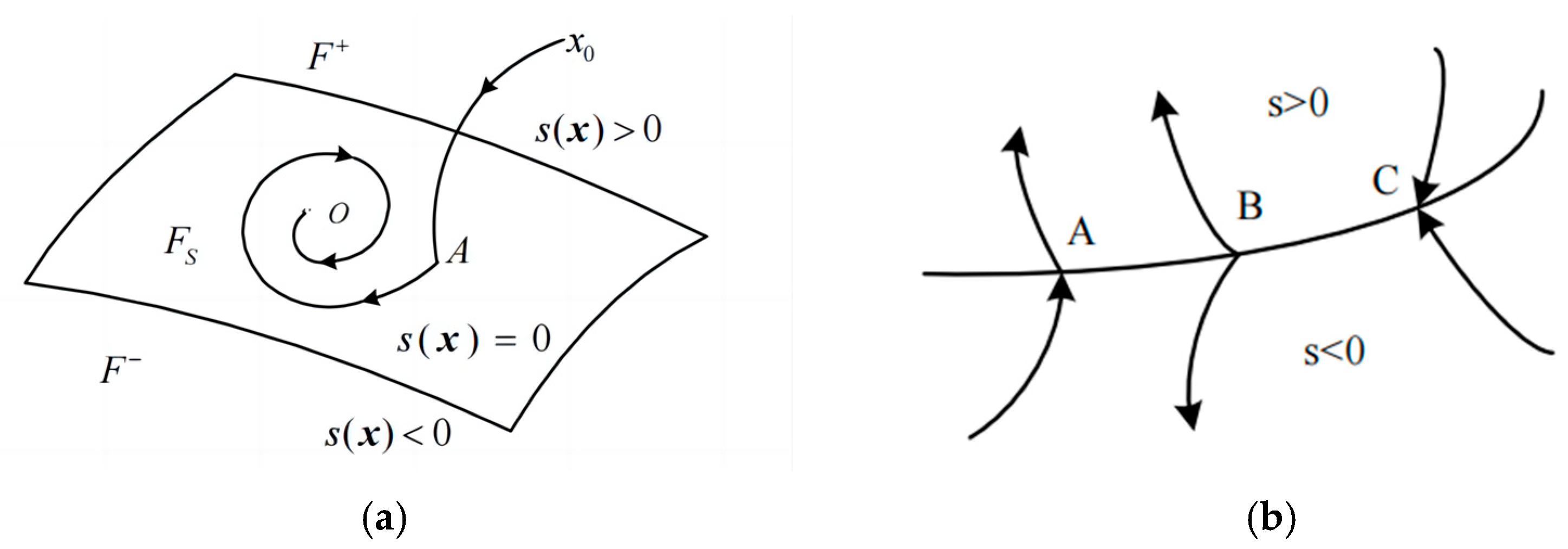
For the sliding-mode control, the first step is to determine the sliding surface and select the appropriate sliding-surface function, s(x). Under the action of different control functions, the trajectory of the system moves differently. As shown in Figure 10a, by designing appropriate control functions, the system can start from an arbitrary initial point, x 0 , in the state space and reach the switching surface (as shown in the x 0 →A section) in a finite time. This process is called the approach section. Once the system trajectory reaches the switching surface, it stays on it and continues to move, and this is called the sliding-mode section (as shown in section A→O). The state of the system moving on the switching surface is called the sliding mode. Since the switching surface is designed according to the expected moving target of the system, no matter how the external parameters change, the system trajectory will eventually reach the preset value on the switching surface [40,41,42,43].
In the state space, take s(x) = 0 as the sliding surface, which represents the state, as shown in Figure 10b. The space is divided into two: s(x) > 0 and s(x) < 0. The motion points on the sliding surface can be divided into three categories:
  • Usually Point A: After the system moves near the sliding surface, it will pass through this point;
  • Starting Point B: After the system motion point reaches the vicinity of the sliding surface, it leaves from both sides of that point;
  • Termination Point C: The system moves towards this point from the upper and lower sides of the sliding surface.
In the study of sliding-mode control, the first two types of motion points have little significance for system control and are generally ignored. If a certain area on the sliding-mode surface is all termination points, it means that once the system state moves near that area, it will be attracted to the area, and this area is therefore called the “sliding mode area”. Due to the fact that all points on the sliding-mode area are termination points, when the system moves near the sliding surface, there will inevitably be lim s 0   s s ˙ < 0 [44,45,46].
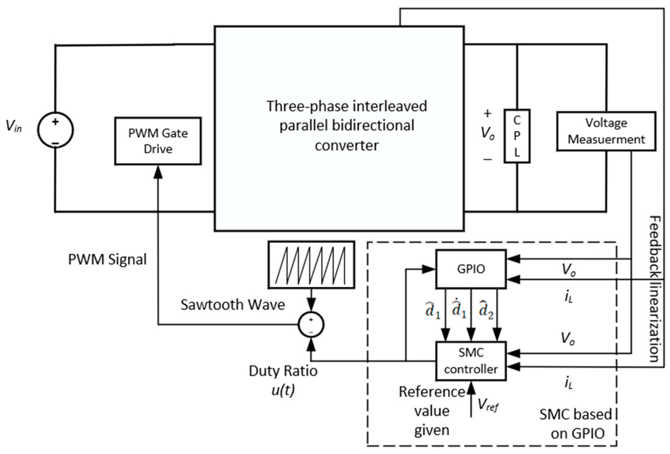
The specific system control is shown in 
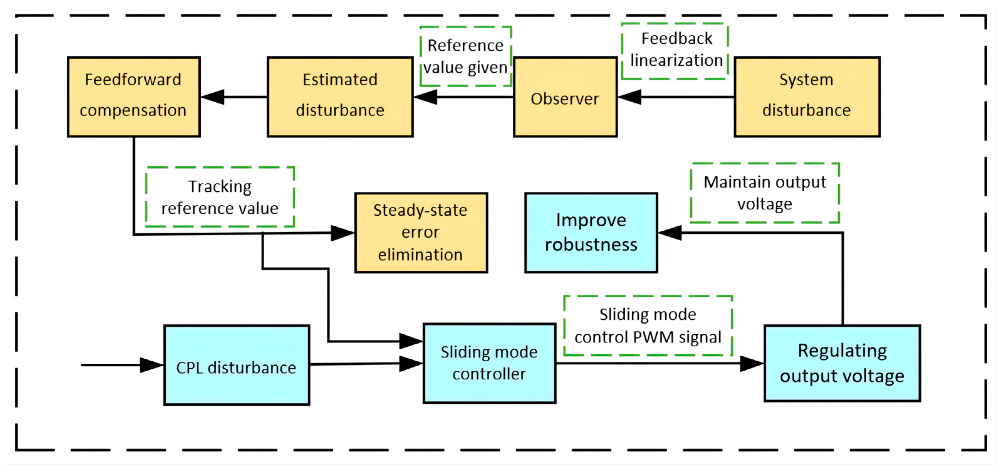
Figure 11. The system block diagram includes four parts: two generalized proportional integral observers, a sliding-mode controller, a pulse width modulator (PWM), and a three-phase interleaved parallel DC/DC converter. The system works as follows: Firstly, two generalized proportional integral observers are constructed based on the feedback values of inductance current and output voltage, and the matched and unmatched disturbances are estimated, respectively. Then, a sliding-mode controller is designed using the estimated values. The controller is compared with the sawblade wave to obtain a PWM wave, and the switching tube of the DC step-down converter is controlled by the PWM wave. The converter can output the desired voltage stably.

3.3. GPI Observer Design

The voltage tracking accuracy of the DC-DC converter system will be affected by disturbances, such as input voltage fluctuation, parameter uncertainty, load resistance disturbance, etc. An effective method to eliminate these disturbances is to introduce disturbance estimation to compensate accurately. For the Buck converter, two generalized integral observers are designed to estimate the matched disturbance and the unmatched disturbance, respectively, and the disturbance estimation is introduced into the design of the control law to compensate for the influence of these disturbances and uncertainties. The specific design of the two generalized proportional integral observers is as follows. The GPI observer of CPL perturbation based on the Buck converter can be constructed as follows:
x ˙ 1 = x 2 + d ^ 1 + h 11 x 1 x ^ 1 d ^ ˙ 1 = d ˙ ^ 1 + h 12 x 1 x ^ 1 d ^ ˙ 1 n 1 = d ^ 1 n + h 1 n x 1 x ^ 1 d ^ ˙ 1 n = h 1 n + 1 x 1 x ^ 1 ,
where d ^ 1 n is an estimated value of the nth order derivative of d 1 , and h 1 i  (i = 1, 2, …, n + 1) represents the parameters to be determined.
To estimate the input voltage disturbance, d 2 (t), another GPI observer is constructed:
{ x ^ ˙ 2 = u LC v in 0 x 1 + v ref LC x 2 R L C + z 2 + h 21 x 2 x ^ 2 d ^ ˙ 2 = d ˙ 2 + h 22 x 2 x ^ 2 d ^ ˙ 2 m 1 = d ^ 2 m + h 2 m x 2 x ^ 2 d ^ ˙ 2 m = h 2 m + 1 x 2 x ^ 2 ,
where d ^ 2 m is an estimated value of the nth order derivative of d 2 , and h 2 j (j = 1, 2, …, m + 1) represents the parameters to be determined.
According to Equations (9) and (10), the uncertainties (i = 1, 2) are related to the power of constant power load, so from a practical point of view, their values and derivatives should be bounded.
In a steady state, the power of the constant power load is considered constant. Therefore, the following assumptions can be made:
The uncertain variables, d i and d ˙ i , of the system (i = 1, 2) meet the following two conditions [47]:
d i t L , d ˙ i t L lim t   d i n = 0 ,
According to Equation (8), the uncertain term is defined by the following:
d ^ 1 = l 1 x 1 p 1 p ˙ 1 = x 2 + d ^ 1 ,
where p 1 is the auxiliary state of the observer, and l 1 is a normal number that is expressed as the observer gain. Similarly, the uncertainty term is given by the following:
d ^ 2 = l 2 x 2 p 2 p ˙ 2 = u LC v in 0 x 1 + v ref LC x 2 R L C + d ^ 2 ,
where p 2 is the observer’s auxiliary state, and l 2 is a normal number that is expressed as the observer gain.
Based on Equations (12) and (13), the standard model and observer estimate of the load power can be provided according to the sliding-mode control design of the proposed composite controller. Them we take the switching function of the system as follows:
s = k 1 x 1 + x 2 + d ^ 1 s ˙ = k 1 x 2 + d 1 + x ˙ 2 + d ^ ˙ 1 ,
where k 1 > 0 is a parameter to be selected.
As a high-order sliding-mode algorithm, the realization of the high-order sliding-mode algorithm usually requires the derivative of sliding-mode variables, while the super-distortion algorithm is a second-order sliding-mode algorithm in nature, so its realization does not require the derivative of sliding-mode variables, thus simplifying the controller structure. Through the design of the control rate, the sliding-mode variable structure rapidly converges within a limited time [30].
The general form of the super-twisting algorithm is as follows:
da 1 dt = λ a 1 1 2 sign a 1 + a 2 + ρ 1 da 2 dt = csign a 1 + ρ 2 ,
In Equation (16), a 1 and a 2 are the state variables; λ and c are the positive constants; and ρ 1 and ρ 2 are the disturbance quantities.
In order to weaken chattering, saturation function is often used to replace the sign function [48]. The form of saturation function is as follows:
sat s , δ = s δ           s δ sign s         s > δ ,
By combining Equations (18) and (19), the form of the super-twisting algorithm becomes the following:
u sta = α s 1 2 sat s + ω d ω dt = β sat s ,
When the super-twisting algorithm is used to design the sliding-mode control function, let ω = a 2 + ρ 1 , and α , β are the parameters to adjust the dynamic velocity and set the steady-state error, respectively. Among them, the parameters α , β affect the convergence rate of the sliding-mode surface. In general, the system can reach the sliding-mode surface faster by taking a larger value and a smaller value.
When the first derivative of the sliding-mode surface is zero, the switching signal, u , is equivalent to a continuous value, u eq .
u eq = LC v in 0 k 1 x 2 + d ^ 1 x 1 + v ref LC x 2 R L C + d ^ 2 + d ˙ ^ 1 + η sat s ,
where the control parameter, k 1 > 0, and the switching gain, η > 0, are the parameters to be designed. Then, the total switch signal, u , is as follows:
u = u eq + u sta ,
where u eq is used to ensure that the trajectory of the system phase is maintained on the sliding-mode surface, and u sta is used to overcome the disturbance effect and to ensure the robustness of the system. The following proves the existence and accessibility of the switching surface, and the Lyapunov function is used to analyze the switching function, so as to enable the stability of the controller’s control voltage and the state curve to quickly converge to the sliding surface.

4. Controller Stability Analysis

Theorem 1.
Consider a DC-DC converter system with both CPL and supply voltage perturbations and combine Equation (14). Under the proposed control law (21), the effect of the time-varying perturbation is removed from the output voltage channel, provided that the switching gain, η > ( k 1 e 1 + e 2 + e 3 ), and the observer parameters in selected Equations (12) and (13) are appropriate, such that (25) is the Hurwitz matrix.
Proof of Theorem 1.
For the GPI observer, the estimated error is defined as e 1 = d 1 d ^ 1 , e 2 = d 2 d ^ 2 , and e 3 = d ^ ˙ 1 d ˙ ^ 1 . The upper bound of the estimation error is defined as e i , (i = 1, 2, 3). Then, the estimated error of the observer can be expressed as follows:
e 11 = x 1 x ^ 1 e 12 = d 1 d ^ 1 e 1 n = d 1 n 1 d ^ 1 n 1 e 1 n + 1 = d 1 n d ^ 1 n ,
e 21 = x 2 x ^ 2 e 22 = d 2 d ^ 2 e 2 m = d 2 m 1 d ^ 1 m 1 e 2 m + 1 = d 2 m d ^ 1 m ,
where e = [ e 11   e 12 e 1 n + 1   e 21   e 22 e 2 m + 1 ] T takes the derivative of the estimate error. Then, the observer error can be dynamically expressed as follows:
e ˙ = H e e + d ˙ ,
where d ˙ = 0   0 d 1 i   0   0 d 2 j T
H e = H e 1 0 0 H e 2 ,
H e 1 = h 11 1 0 0 h 12 0 1 0 h 1 n 0 0 1 h 1 n + 1 0 0 0 0 ,
H e 2 = h 21 1 0 0 h 22 0 1 0 h 2 m 0 0 1 h 2 m + 1 0 0 0 0 ,
By selecting parameters correctly in the GPI observer, we can get the Hurwitz stability matrix; that is, the state matrix of the system is the Hurwitz matrix. Then, the error dynamic is asymptotically stable, which means the following:
lim t   e i = d i d ^ i = 0 , i = 1 , 2 ,
Take the Lyapunov function as follows:
V = 1 2 s 2 ,
V ˙ = s s ˙ ,
Substituting (17) and (22) into (28) gives the following:
V ˙ = η s + k 1 e 1 + e 2 + e 3 s + v in 0 LC u sta s η k 1 e 1 + e 2 + e 3 s + v in 0 LC u sta s 2 η k 1 e 1 + e 2 + e 3 V 1 2 + v in 0 LC u sta s
where the coefficient α > 0 , β > 0 of u sta can be seen from Equation (17); when s < 0, u sta > 0, and when s > 0, u sta < 0. Then, when the switching gain η > ( k 1 e 1 + e 2 + e 3 ) meets the condition, it is satisfied, V ˙ < 0. According to Lyapunov’s sliding-mode reachability condition, the system can reach the designed sliding-mode surface in a finite time. The system state will reach the defined sliding surface, s = 0, in a finite time.
By integrating Equations (11) and (17), we obtain the following:
x ˙ 1 = k 1 x 1 d 1 d ^ 1 ,
According to Reference [18], if the following system exists,
x ˙ = f t , x , u , x R , u R ,
when the system input reaches stability, if the input signal meets lim t   u = 0 , then the states satisfy lim t   x = 0 . According to Equations (26) and (17), lim t   e 1 = 0 , k 1 > 0 . It is easy to arrive at the conclusion that the voltage tracking error converges asymptotically to zero along the sliding surface, thus completing the proof. Similarly, the Boost mode is a similar proof. □

5. Simulation Results and Analysis

In order to verify whether the proposed method has a faster convergence rate and load-resistance performance, for Buck converters with matched and unmatched disturbances, the proposed method was simulated and compared with the control methods in other works from the literature under the condition that the circuit parameters are the same. The results show that the proposed method can effectively suppress the influence of perturbation and ensure the stability of output voltage. It can improve the anti-interference performance of the whole system.

5.1. Simulation Model Construction

The simulations are conducted in Simulink, using GPI observers to estimate the state and lumped disturbances of the system. Then, the estimated values of the observers are introduced into the controller for feedforward compensation, achieving fast and accurate tracking of the output voltage to the reference voltage. Select the input and output voltage, use the inductance current as feedback variables, and perform a high-order sliding-mode control algorithm to limit the calculated amplitude to prevent the switch from being in a continuous on or off state. Build a simulation model of a three-phase interleaved parallel bidirectional DC/DC converter in Simulink and write a sliding-mode control algorithm through the MATLAB function. The circuit uses ideal components, and the simulation diagram is shown in Figure 12.

5.2. Set System Parameters

The control objective of this simulation experiment is, under the same circuit system, sequentially use two methods to control, observe, and analyze the value of each state variable with time from the figure, compare the transient performance and resistance of the system under the control of the two methods’ interference performance. In order to ensure the fairness of the comparison, the two methods should be simulated and compared under the same converter circuit system.
The effectiveness of the proposed control strategy is verified by the following simulation. The parameter values of the simulation experiment are shown in Table 3. To further illustrate the advantages, this paper compares the NDO-Integral SMC scheme with the GPIO-SMC scheme. A MATLAB simulation is used to compare the two methods:
In Method 2, the switching function of the system can be designed as follows:
s = k 1 x 1 + x 2 + d 1 + k 2 0 t x 1 dt s ˙ = k 1 x 2 + d 1 + x ˙ 2 + d 1 ˙ + k 2 x 1 ,
Then, the switching signal is as follows:
u = LC v in 0 k 1 x 2 + d ^ 1 x 1 + v ref LC x 2 R L C + d ^ 2 + d 1 ˙ + k 2 x 1 + η sat s ,
Since the observers used for load estimation provide composite controller reference values, it is necessary to first design their parameters to ensure that the observers can accurately estimate the power of the load. The size of gain l 1 and l 2 will affect the accuracy of the observer in tracking load power. In order to investigate the tracking effect of the l 1 size on the observer’s load power, the parameters k 1 , k 2 , and l 2 are first fixed to 200, 1000, and 200, respectively, and the observer’s observation effect is observed by setting different values. As shown in Figure 13a, when the CPL power jumps from 5 W to 10 W, the observer can quickly track the fluctuation of load power as the gain l 1 increases. The gain l 1 can be set to 1000.
The same settings k 1 = 200 and k 2 = 1000 , fix l 1 at 1000, and different values of l 2 will be set to observe the impact of their magnitude on the performance of load power fluctuation estimation. From Figure 13b, we can see that when l 2 < 2000 , as l 2 increases, the observer’s tracking effect on load power fluctuations remains almost unchanged. However, when l 2 < 2000 , the observer was unable to accurately estimate the fluctuation of load power. To prevent the observer from being unable to track load-power fluctuations, the gain l 2 was set to 200.
Afterwards, it is necessary to adjust the relevant parameters of the composite controller. To obtain the impact of parameter changes on the DC bus voltage, first fix k 1 at 200 and observe the fluctuation of DC bus voltage by setting different values of k 2 , as shown in the Figure 14. From Figure 14a, it can be seen that, as k 2 increases, the time it takes for the bus voltage to recover to its steady-state value becomes shorter. However, when k 2 exceeds 1000, the time it takes for the bus voltage to recover to the stable value does not change, so k 2 will be set at 1000.
After obtaining l 1 , l 2 , and k 2 , analyze the impact of their values on the DC bus voltage by setting different k 1 values. From Figure 14b, it can be seen that as k 1 gradually increases, the fluctuation amplitude of the DC bus voltage increases. When k 1 = 1000, the DC bus voltage even exhibits oscillation, so k 1 can be set at 100.

5.3. Analysis of Simulation Examples

5.3.1. Keep the Constant Power Load and Change the Load Resistance

The load resistance experiences a sudden change during the simulation; that is, the resistance drops from 20 Ω to 10 Ω at 0.04 s and then rises to 20 Ω at 0.08 s.
For three-phase interleaved parallel converter systems with matched and unmatched disturbances, as shown in Figure 15a, both methods can make the output voltage rapidly approach the set reference value, and there is no steady-state error in the output voltage. However, it is clear from Figure 15a that the output voltage response time of Method 1 and Method 2 is about 0.005 s and 0.009 s, respectively, so Method 1 has a faster convergence speed. As shown in Figure 15b, although the overshoot of the inductance current in Method 1 is greater than that in Method 2, the rise time and adjustment time of Method 1 are about 0.002 s and 0.004 s respectively. Both are less than the rise time and adjustment time of Method 2. As shown in the controller output in Figure 15c, the response speed of controller output, u, in Method 1 is higher than that in Method 2, and the convergence time of the controller is shorter.
Figure 16a,b capture the estimation effect of the GPI observer on the unmatched disturbance and the matched disturbance, respectively. From the comparison results in Table 4, it can be seen that at the moment 0.04 s, the resistance drops from 20 Ω to 10 Ω, and the estimated convergence time of the observer’s sum is 0.014 s and 0.006 s, respectively. The resistance increases from 10 Ω to 20 Ω at 0.08 s, and the convergence time of the observer is 0.012 s and 0.007 s, respectively. It can be seen that when the load resistance changes abruptly, the GPI observer can quickly track the value of the disturbance and make an accurate estimation of and match the disturbance, thus further proving that the GPI observer has strong adaptability to the resistance load change in the system; that is, the observer has a fast response speed and good accuracy when estimating the system interference.

5.3.2. Keep the Load Resistance and Change the Constant Power Load

The constant load power was changed during the simulation; that is, CPL rose from 6 W to 8 W at 0.04 s and then dropped to 6 W at 0.08 s.
As can be seen from the output voltage response curve in Figure 17a, Method 1 not only minimizes the voltage drop but also minimizes the recovery time. Although Method 2 can also keep the system stable, it sacrifices control performance to some extent. From the inductor current curve in Figure 17b, it can be seen that the recovery speed of the Method 1 curve is significantly faster than that of Method 2. As shown in the controller output of Figure 17c, the response and convergence speed of the controller output, u, of Method 1 are higher than those of Method 2.
As shown in Figure 18, the convergence time of the observer pairs and estimates are 0.015 s and 0.007 s, respectively. At 0.08 s, the power of the constant power load decreases from 8 W to 6 W, and the convergence time of the observer is 0.014 s and 0.007 s, respectively. The GPI observer can quickly track the value of the disturbance and make accurate estimates of and match the disturbance.
In short, from the comparison results in Table 5, it can be seen that the converter under the control of Method 1 has a faster output voltage response, better transient performance, and greater anti-disturbance ability.

6. Conclusions

Aiming at the precise power control of three-phase interleaved bidirectional converters in a DC microgrid under the variation of supply voltage and constant power load, a GPI observer sliding-mode control method based on a super-twisting algorithm was proposed. The proposed high-order sliding-mode control strategy can stabilize the output voltage at the expected CPL power value and generate errors between the inductance current and the output voltage of the converter on the sliding-mode surface. By combining the interference estimations, smaller switching gains can be achieved without sacrificing interference suppression, thus ensuring the stability of the output voltage.
Finally, the effectiveness of the control algorithm was verified by comparing the simulation results of the proposed control method with the classical method. The transient recovery index and anti-interference capability of the controller were further improved. The results show that the proposed method can ensure that the output voltage of the system converges to the reference voltage, and this controller further improves the transient recovery index, anti-interference ability, and vibration-reduction performance of the system. The advantage of the controller is that it can quickly improve the rate of convergence of the system state, which is the disadvantage of the traditional observer.

Author Contributions

Y.J. and D.W. described the proposed framework and wrote the whole manuscript; Y.L. implemented the simulation experiments; G.S. and K.S. collected data; Y.J. and Y.N. revised the manuscript. All authors have read and agreed to the published version of the manuscript.

Funding

This research is supported in part by the Natural Science Foundation of China, under Grant 52077027 Study, and in part by the Liaoning Province Science and Technology Major Project No. 2022021000014.

Institutional Review Board Statement

Not applicable.

Informed Consent Statement

Not applicable.

Data Availability Statement

The data presented in this study are available upon request from the corresponding author.

Acknowledgments

The authors thank the chief editor and the reviewers for their valuable comments on how to improve the manuscript.

Conflicts of Interest

The authors declare no conflict of interest.

References

  1. Emadi, A.; Khaligh, A.; Rivetta, C.H.; Williamson, G.A. Constant power loads and negative impedance instability in automotive systems: Definition, modeling, stability, and control of power electronic converters and motor drives. IEEE Trans. Veh. Technol. 2006, 55, 1112–1125. [Google Scholar] [CrossRef]
  2. Wang, Z.; Li, S.; Yang, J.; Li, Q. Current sensorless finite-time control for Buck converters with time-varying disturbances. Control Eng. Pract. 2018, 77, 127–137. [Google Scholar] [CrossRef]
  3. Yang, J.; Cui, H.; Li, S.; Zolotas, A. Optimized active disturbance rejection control for DC-DC Buck converters with uncertainties using a reduced-order GPI observer. IEEE Trans. Circuits Syst. I Reg. Pap. 2018, 65, 832–841. [Google Scholar] [CrossRef] [Green Version]
  4. Zolfi, P.; Vahid, S.; EL-Refaie, A. Development of A Family of High Voltage Gain Step-Up Multi-Port DC-DC Converters for Fuel Cell-based Hybrid Vehicular Power Systems. In Proceedings of the 2022 24th European Conference on Power Electronics and Applications (EPE’22 ECCE Europe), Hanover, Germany, 5–9 September 2022; pp. 1–11. [Google Scholar]
  5. Zheng, C.; Dragičević, T.; Zhang, J.; Chen, R.; Blaabjerg, F. Composite Robust Quasi-Sliding Mode Control of DC–DC Buck Converter with Constant Power Loads. IEEE J. Emerg. Sel. Top. Power Electron. 2021, 9, 1455–1464. [Google Scholar] [CrossRef]
  6. Singh, S.; Gautam, A.R.; Fulwani, D. Constant power loads and their effects in DC distributed power systems: A review. Renew. Sustain. Energy Rev. 2017, 72, 407–421. [Google Scholar] [CrossRef]
  7. Ding, S.; Zheng, W.X.; Sun, J.; Wang, J. Second-order sliding-mode controller design and its implementation for buck converters. IEEE Trans. Ind. Inform. 2018, 14, 1990–2000. [Google Scholar] [CrossRef]
  8. Lin, X.; Liu, J.; Liu, F.; Liu, Z.; Gao, Y.; Sun, G. Fractional-Order Sliding Mode Approach of Buck Converters with Mismatched Disturbances. IEEE Trans. Circuits Syst. I Regul. Pap. 2021, 68, 3890–3900. [Google Scholar] [CrossRef]
  9. Pawar, S.N.; Chile, R.H.; Patre, B.M. Design of generalized extended state observer based control for nonlinear systems with matched and mismatched uncertainties. In Proceedings of the 2017 Indian Control Conference (ICC), Guwahati, India, 4–6 January 2017. [Google Scholar]
  10. Gao, Z.; Liu, X.; Chen, Z.Q. Unknown input observer—Based robust fault estimation for systems corrupted by partially decoupled disturbances. IEEE Trans. Ind. Electron. 2016, 63, 2537–2547. [Google Scholar] [CrossRef] [Green Version]
  11. Wang, Z.; Li, S.; Wang, J.; Li, Q. Robust control for disturbed Buck converters based on two GPl observers. Control Eng. Pract. 2017, 66, 13–22. [Google Scholar] [CrossRef]
  12. Wang, Z.; Li, S.; Wang, J.; Li, Q. Generalized proportional integral observer based backstepping control for DC-DC Buck converters with mismatched disturbances. In Proceedings of the IEEE International Conference on Industrial Technology, Taipei, Taiwan, 14–17 March 2016; pp. 1783–1789. [Google Scholar]
  13. Jeung, Y.-C.; Lee, D.-C.; Dragičević, T.; Blaabjerg, F. Design of Passivity-Based Damping Controller for Suppressing Power Oscillations in DC Microgrids. IEEE Trans. Power Electron. 2021, 36, 4016–4028. [Google Scholar] [CrossRef]
  14. Jianguo, G.; Ningbo, L.; Shengjiang, Y.; Jun, Z. A New Adaptive Sliding Mode Control for A Mismatched Second-order System. In Proceedings of the 2020 Chinese Control and Decision Conference (CCDC), Hefei, China, 22–24 August 2020. [Google Scholar]
  15. Shtessel, Y.; Edwards, C.; Fridman, L.; Levant, A. Sliding Mode Control and Observation; Springer: New York, NY, USA, 2013. [Google Scholar]
  16. Chen, W.-H.; Yang, J.; Guo, L.; Li, S. Disturbance-observer-based control and related methods-An overview. IEEE Trans. Ind. Electron. 2016, 63, 1083–1095. [Google Scholar] [CrossRef] [Green Version]
  17. Xu, X.; Liu, Q.; Zhang, C.; Zeng, Z. Prescribed performance controller design for DC converter system with constant power loads in DC microgrid. IEEE Trans. Syst. Man Cybern. Syst. 2018, 50, 4339–4348. [Google Scholar] [CrossRef]
  18. Xu, Q.; Zhang, C.; Wen, C.; Wang, P. A novel composite nonlinear controller for stabilization of constant power load in DC microgrid. IEEE Trans. Smart Grid 2019, 10, 752–761. [Google Scholar] [CrossRef]
  19. Wang, H.; Han, M.; Han, R.; Guerrero, J.M.; Vasquez, J.C. A Decentralized Current-Sharing Controller Endows Fast Transient Response to Parallel DC–DC Converters. IEEE Trans. Power Electron. 2018, 33, 4362–4372. [Google Scholar] [CrossRef] [Green Version]
  20. Zhang, B. Research on Equal Current Sharing Parallel Connection Technology of Multiple Converters in Ship DC Microgrid; Dalian Maritime University: Dalian, China, 2020. [Google Scholar]
  21. Zhang, Q.; Zhuang, X.; Liu, Y.; Guo, H.; Wang, C. A DC Microsource Parallel Current Sharing Control Strategy Based on Line Impedance Compensation. Grid Technol. 2021, 45, 1912–1921. [Google Scholar]
  22. Foley, R.F.; Kavanagh, R.C.; Egan, M.G. Sensorless Current Estimation and Sharing in Multiphase Buck Converters. IEEE Trans. Power Electron. 2012, 27, 2936–2946. [Google Scholar] [CrossRef]
  23. Xia, J.; Li, Z.; Gao, X.; Guo, Y.; Zhang, X. Real-Time Sensor Fault Identification and Remediation for Single-Phase Grid-Connected Converters Using Hybrid Observers with Unknown Input Adaptation. IEEE Trans. Ind. Electron. 2023, 70, 2407–2418. [Google Scholar] [CrossRef]
  24. Hao, W.; Lin, X.; Chen, W.; Ji, Y.; Jing, F.; Gao, Y.; Wang, Z.; Liu, J. Disturbance Observer Based Back-Stepping Control for Buck Converters with Unmatched Disturbances: An RBF Neural Network Approach. In Proceedings of the 2022 China Automation Congress (CAC), Xiamen, China, 25–27 November 2022; pp. 3335–3340. [Google Scholar] [CrossRef]
  25. Wu, B.; Yang, J.; Wang, J.; Li, S. Extended state observer based control for DC-DC buck converters subject to mismatched disturbances. In Proceedings of the 33rd Chinese Control Conference, Nanjing, China, 28–30 July 2014; pp. 8080–8085. [Google Scholar] [CrossRef]
  26. Nan, Y.R.; Yang, C.B.; Lv, W.J. ESO based Approach Law Control of Buck Converter. Comput. Meas. Control 2020, 28, 84–88. [Google Scholar]
  27. Nan, Y.; Chen, S.; Wang, S. Buck type converter approach law control based on GPI observer. Comput. Meas. Control 2021, 29, 89–94. [Google Scholar] [CrossRef]
  28. Dehri, K.; Nouri, A.S. A discrete repetitive adaptive sliding mode control for DC-DC buck converter. Proc. Inst. Mech. Eng. I J Syst. Control. Eng. 2021, 235, 1698–1708. [Google Scholar] [CrossRef]
  29. Boukerdja, M.; Chouder, A.; Hassaine, L.; Bouamama, B.O.; Issa, W. H∞ based control of a DC/DC Buck converter feeding a constant power load in uncertain DC microgrid system. ISA Trans. 2020, 105, 278–295. [Google Scholar] [CrossRef] [PubMed]
  30. Fulwani, D.; Singh, S. Mitigation of Negative Impedance Instabilities in DC Distribution Systems; Springer: Singapore, 2017. [Google Scholar]
  31. Utkin, V.; Poznyak, A.; Orlov, Y.; Polyakov, A. Conventional and high order sliding mode control. J. Frankl. Inst. 2020, 357, 10244–10261. [Google Scholar] [CrossRef]
  32. Young, K.D.; Utkin, V.I.; Ozguner, U. A control engineer’s guide to sliding mode control. IEEE Trans. Control Syst. Technol. 1999, 7, 328–342. [Google Scholar] [CrossRef] [Green Version]
  33. Utkin, V. Sliding mode control. In Control Systems, Robotics and Automation–Volume XIII: Nonlinear, Distributed, and Time Delay Systems-II; EOLSS: Abu Dhabi, United Arab Emirates, 2009; p. 130. [Google Scholar]
  34. Şahın, M.E.; Okumuş, H.İ.; Kahvecı, H. Sliding mode control of PV powered DC/DC Buck-Boost converter with digital signal processor. In Proceedings of the 2015 17th European Conference on Power Electronics and Applications (EPE’15 ECCE-Europe), Geneva, Switzerland, 8–10 September 2015; pp. 1–8. [Google Scholar]
  35. Chen, Z.X.; Wang, J.; Ge, L.S.; Jiang, T.; Liu, Y.-F.; Liu, Y.-F. Double Integral Sliding Mode Control of Paralleled DC-DC Converters. In Proceedings of the Conference on Industrial Electronics and Applications (ICIEA), Auckland, New Zealand, 15–17 June 2015. [Google Scholar]
  36. Wang, Y.; Xia, H.; Cao, Y. Voltage Controller of DC-DC Buck Converter Using Terminal Sliding Mode. In Proceedings of the IECON 2015—41st Annual Conference of the IEEE Industrial Electronics Society, Yokohama, Japan, 9–12 November 2015. [Google Scholar]
  37. Fossas, E.; Ras, A. Second-order Sliding-mode Control of a Buck Converter. In Proceedings of the 41st IEEE Conference on Decision and Control, Las Vegas, NV, USA, 10–13 December 2002. [Google Scholar]
  38. Utkin, V.I.; Poznyak, A.S. Adaptive sliding mode control with application to super twist algorithm: Equivalent control method. Automatica 2013, 49, 39–47. [Google Scholar] [CrossRef]
  39. Zhao, Y.; Qiao, W.; Ha, D. A Sliding-Mode Duty-Ratio Controller for DC/DC Buck Converters with Constant Power Loads. IEEE Trans. Ind. Appl. 2014, 50, 1448–1458. [Google Scholar] [CrossRef] [Green Version]
  40. Yu, X.; Man, Z. Fast Terminal Sliding-mode Control Design for Nonlinear Dynamical Systems. IEEE Trans. Circuits Syst. Part I Fundam. Theory Appl. 2002, 49, 261–264. [Google Scholar]
  41. Rui, L.; Yan, D.; Wu, M.; Chai, Y. High-order Sliding-mode Control for DC-DC Converters. In Proceedings of the 2012 7th International Power Electronics and Motion Control Conference (IPEMC 2012), Harbin, China, 2–5 June 2012. [Google Scholar]
  42. Li, S.; Yang, J.; Wu, B.; Li, Q. Finite-Time disturbance observer based nonsingular terminal sliding mode control for PWM-based DC-DC buck converters with mismatched load disturbances. IET Power Electron. 2016, 9, 1995–2002. [Google Scholar]
  43. Zaman, H.; Zheng, X.; Khan, S.; Ali, H.; Wu, X. Hysteresis Modulation-based Sliding Mode Current Control of Z-source DC-DC Converter. In Proceedings of the 2016 IEEE 8th International Power Electronics and Motion Control Conference (IPEMC 2016—ECCE Asia), Hefei, China, 22–26 May 2016. [Google Scholar]
  44. Basin, M.V.; Rodriguez-Ramirez, P.C. Sliding-mode filter design for linear systems with unmeasured states. IEEE Trans. Ind. Electron. 2010, 58, 3616–3622. [Google Scholar] [CrossRef]
  45. Yang, G.; Wang, Y.; Zhao, Y. Observer-Based Non-singular Terminal Sliding Mode Control of Boost converters. In Proceedings of the 2020 39th Chinese Control Conference (CCC), Shenyang, China, 27–29 July 2020; pp. 2096–2100. [Google Scholar]
  46. Wang, Y.; Ying, Z.; Zhang, W. Unified Sliding Mode Control of Boost Converters with Quantitative Dynamic and Static Performances. In Proceedings of the IECON 2020—46th Annual Conference of the IEEE Industrial Electronics Society, Singapore, 18–21 October 2020; pp. 3271–3276. [Google Scholar]
  47. Hu, J.; Wang, Z. Sliding Mode Control for DC-DC Converters with Unknown Constant Power Load in Renewable Energy Systems. In Proceedings of the 2022 7th International Conference on Power and Renewable Energy (ICPRE), Shanghai, China, 23–26 September 2022. [Google Scholar]
  48. Chalanga, A.; Cail Al, S.K.; Fridman, L.; Bandyopadhyay, B.; Moreno, J.A. Implementation of super-twisting Control: Super. The death and higher order Sliding mode observer based printing proaches. IEEE Trasactions Ind. Electmnics 2016, 63, 3677–3685. [Google Scholar] [CrossRef]
Figure 1. DC/DC converters with constant power characteristics in electrical systems.
Sustainability 15 09720 g001
Figure 2. Negative impedance characteristics of constant power load.
Sustainability 15 09720 g002
Figure 3. Changes in DC bus voltage during power fluctuations of different types of loads: (a) constant power load power fluctuation and (b) pure resistance load power fluctuation.
Sustainability 15 09720 g003
Figure 4. Stable and unstable regions based on small signal theory.
Sustainability 15 09720 g004
Figure 5. Topology structure of three-phase interleaved parallel bidirectional DC/DC main circuit.
Sustainability 15 09720 g005
Figure 6. The main waveforms of the three-phase interleaved parallel converter during steady-state operation: (a) the main waveform of 0 < d < 1/3, (b) the main waveform of 1/3 < d < 2/3, and (c) the main waveform of 2/3 < d < 1/3.
Sustainability 15 09720 g006
Figure 7. Equivalent topology diagram of three-phase interleaved converter at different working stages: (I) Switch tubes Q1 and Q2 are turned off, and switch tube Q3 is on. (II) Switch tubes Q1 and Q3 are turned off, and switch tube Q2 is on. (III) Switch tube Q1 is off, switch tubes Q2 and Q3 are on. (IV) Switch tube Q1 is on, switch tubes Q2 and Q3 are off. (V) Switch tubes Q1 and Q3 are on, while switch tube Q2 is off. (VI) Switch tubes Q1 and Q2 are on, while switch tube Q3 is off. (VII) The switch tubes Q1, Q2, and Q3 are conducting. (VIII) The switch tubes Q1, Q2, and Q3 are turned off.
Sustainability 15 09720 g007
Figure 8. Control flowchart of composite controller.
Sustainability 15 09720 g008
Figure 9. Equivalent variable structure model of Boost converter and Buck converter: (a) Boost mode and (b) Buck mode.
Sustainability 15 09720 g009
Figure 10. System motion under sliding-mode control: (a) the motion trajectory of the system on the sliding surface and (b) three types of points on the sliding surface.
Sustainability 15 09720 g010
Figure 11. Control block diagram of the whole system.
Sustainability 15 09720 g011
Figure 12. Sliding-mode control simulation model.
Sustainability 15 09720 g012
Figure 13. Load estimation performance of l 1 and l 2 under different values: (a) load estimation response with different values of l 1 and (b) load estimation response with different values of l 2 .
Sustainability 15 09720 g013
Figure 14. Load estimation performance of k 1 and k 2 under different values: (a) voltage tracking response with different values of k 2 and (b) voltage tracking response with different values of k 1 .
Sustainability 15 09720 g014
Figure 15. Comparison of output responses under load variation: (a) output voltage, (b) inductive current, (c) control input, and (d) load resistance.
Sustainability 15 09720 g015
Figure 16. Estimate of the observer under load variation: (a) estimation of unmatched perturbations, d 1 ; and (b) estimation of matching perturbations, d 2 .
Sustainability 15 09720 g016
Figure 17. Comparison of output responses under CPL variation: (a) output voltage, (b) inductive current, and (c) control input.
Sustainability 15 09720 g017
Figure 18. Estimate of the observer under CPL variation: (a) estimation of unmatched perturbations, d 1 ; and (b) estimation of matching perturbations, d 2 .
Sustainability 15 09720 g018
Table 1. Topology diagram parameters of three-phase interleaved parallel converter.
Topology Diagram Parameters
v in DC source bus voltage
v o DC load bus voltage
iL1, iL2, iL3Inductance current
R L Load resistance
v in 0 Nominal value of DC source bus voltage
R L 0 Nominal value of load resistance
C1, C2Filter capacitor
L1, L2, L3Filter inductance
Q1, Q2, Q3Switch tube components
Table 2. Topology diagram parameters of Buck mode and Boost mode.
Topology Diagram Parameters
v in Input voltage
v o Output voltage
i L Instantaneous inductance current
R L load resistance
C 1 Boost circuit capacitance value
C 2 Buck circuit capacitance value
LInductance value
Table 3. Parameters of simulation system.
DescriptionsParametersValues
Input voltage V in 20 V
Reference voltage V ref 5 V
InductanceL1 × 10−4 H
CapacitanceC1 × 10−3 F
Switching frequency f s 20 kHz
The power of CPLP6 W
Load resistance R L 50 Ω
Table 4. Comparison of dynamic response of the proposed controller under changes in load resistance.
P = 6 W, Vref = 5 V, RL = 10~20 Ω
Method GPIONDOB
Input voltage 20 V20 V
Setting time0.04 s~0.08 s0.04 s~0.08 s
Voltage recovery time0.005 s0.009 s
Current recovery time0.002 s0.004 s
Voltage overshoot0.056 V0.144 V
Current overshoot0.064 A0.102 A
Table 5. Comparison of dynamic response of the proposed controller under CPL changes.
P = 6~8 W, Vref = 5 V, RL = 20 Ω
Method GPIONDOB
Input voltage 20 V20 V
Setting time0.04 s~0.08 s0.04 s~0.08 s
Voltage recovery time0.007 s0.01 s
Current recovery time0.005 s0.009 s
Voltage overshoot0.025 V0.108 V
Current overshoot0.069 A0.078 A
Disclaimer/Publisher’s Note: The statements, opinions and data contained in all publications are solely those of the individual author(s) and contributor(s) and not of MDPI and/or the editor(s). MDPI and/or the editor(s) disclaim responsibility for any injury to people or property resulting from any ideas, methods, instructions or products referred to in the content.

