
Efficient Multi-Phase Converter for E-Mobility

 , , , and
Abstract
:1. Introduction
- ○
- The output power and output voltage of the presented converter are 33.38 kW and 500 V. The inductor ripple current is reduced by 25.76%, hence the size and cost of the inductor are also less compared to the existing converter, such as BC and IBC.
- ○
- Circuit size reduces due to the reduction in the size of the passive components, which is a major advantage for the EV model.
- ○
- Based on the interleaved techniques the total power loss is reduced and the total inductor current is reduced by 26.92% compared to the existing converter.
- ○
2. Multi-Phase Interleaved Boost Converter
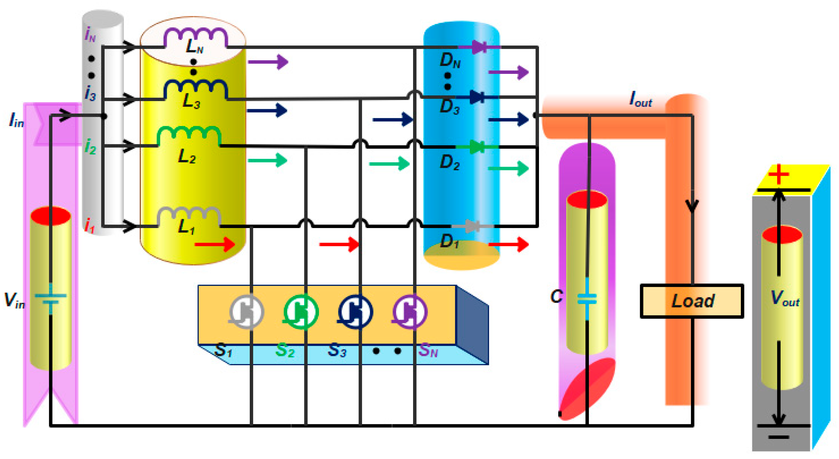
2.1. N Phase IBC Schematic Diagram
2.2. Design Parameter Calcultaion
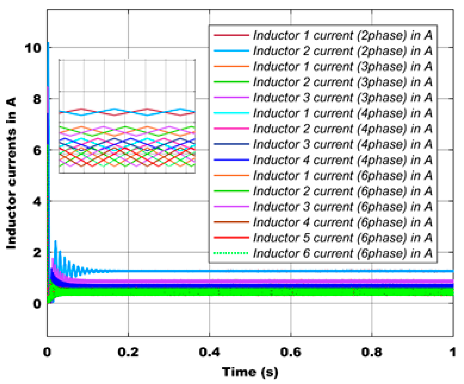
3. MPIBC Simulation Result and Discussion
Power Loss and Efficiency Calculation of MPIBC
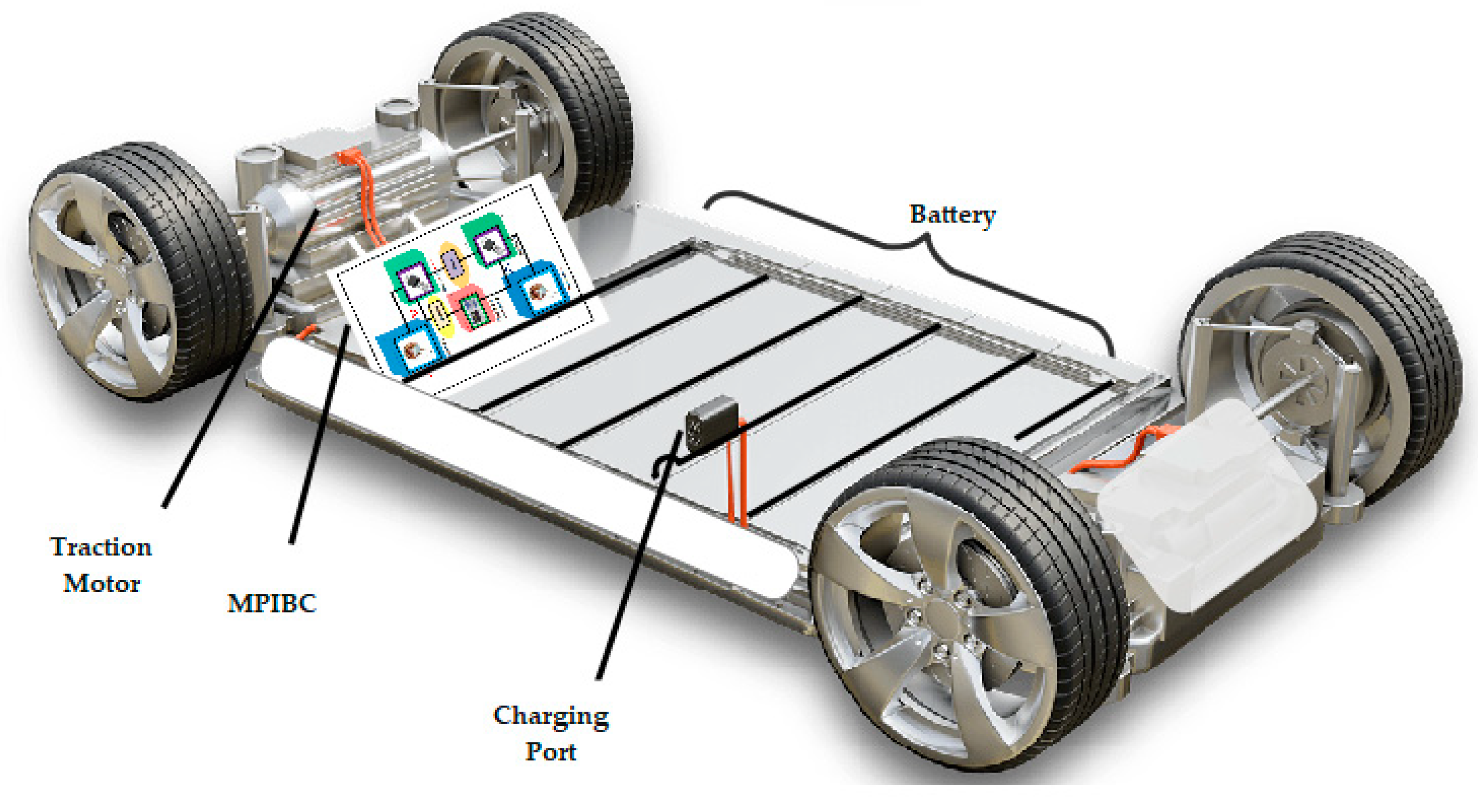
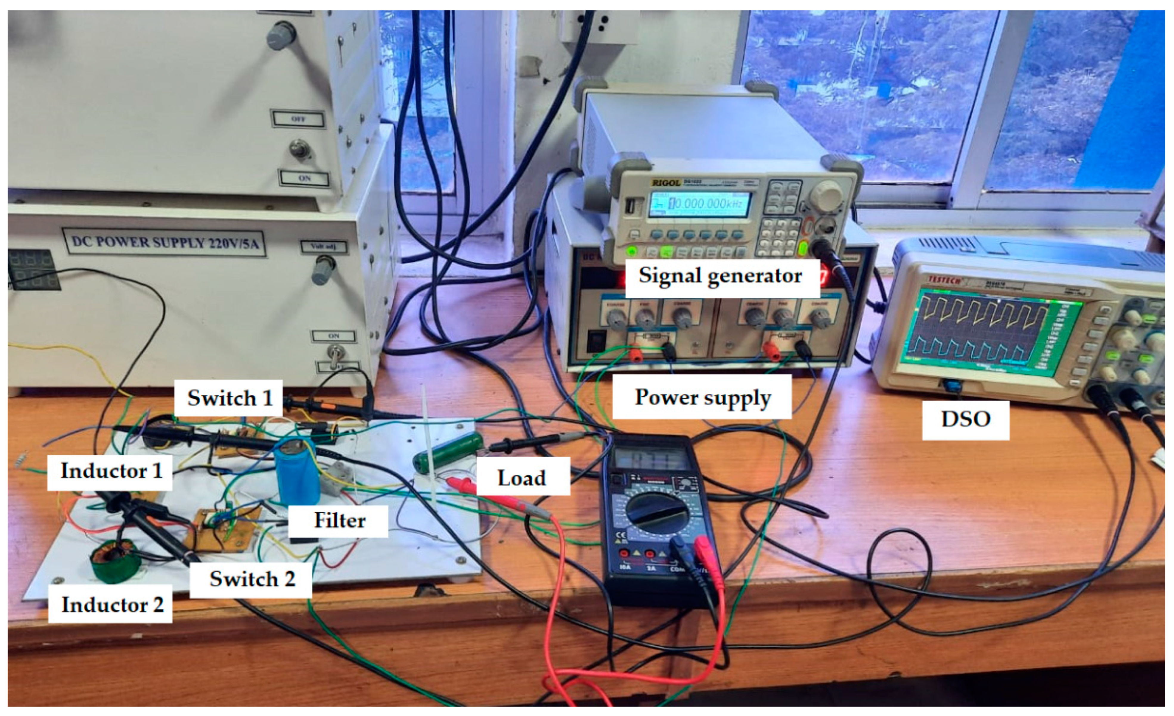
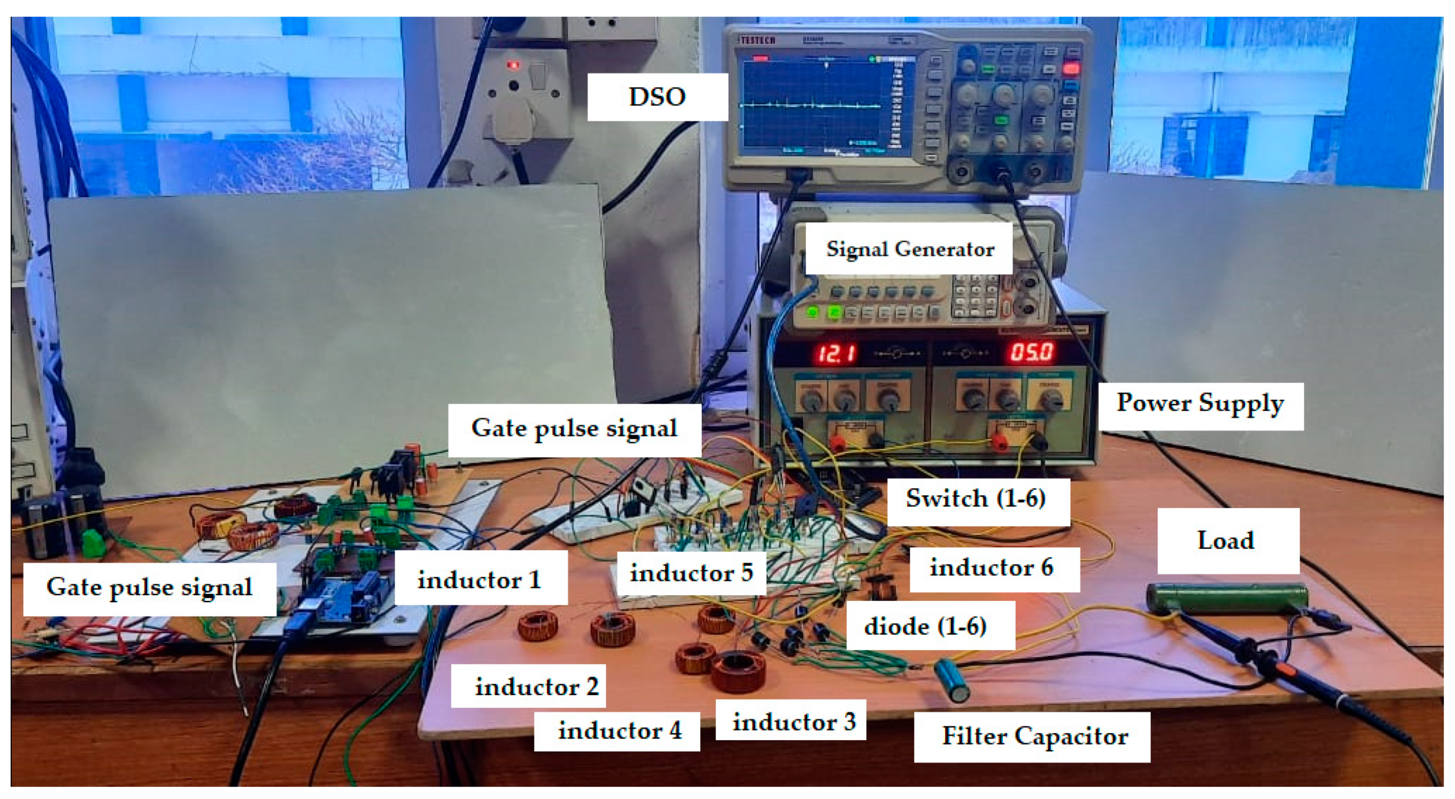
4. Hardware Setup for MPIBC
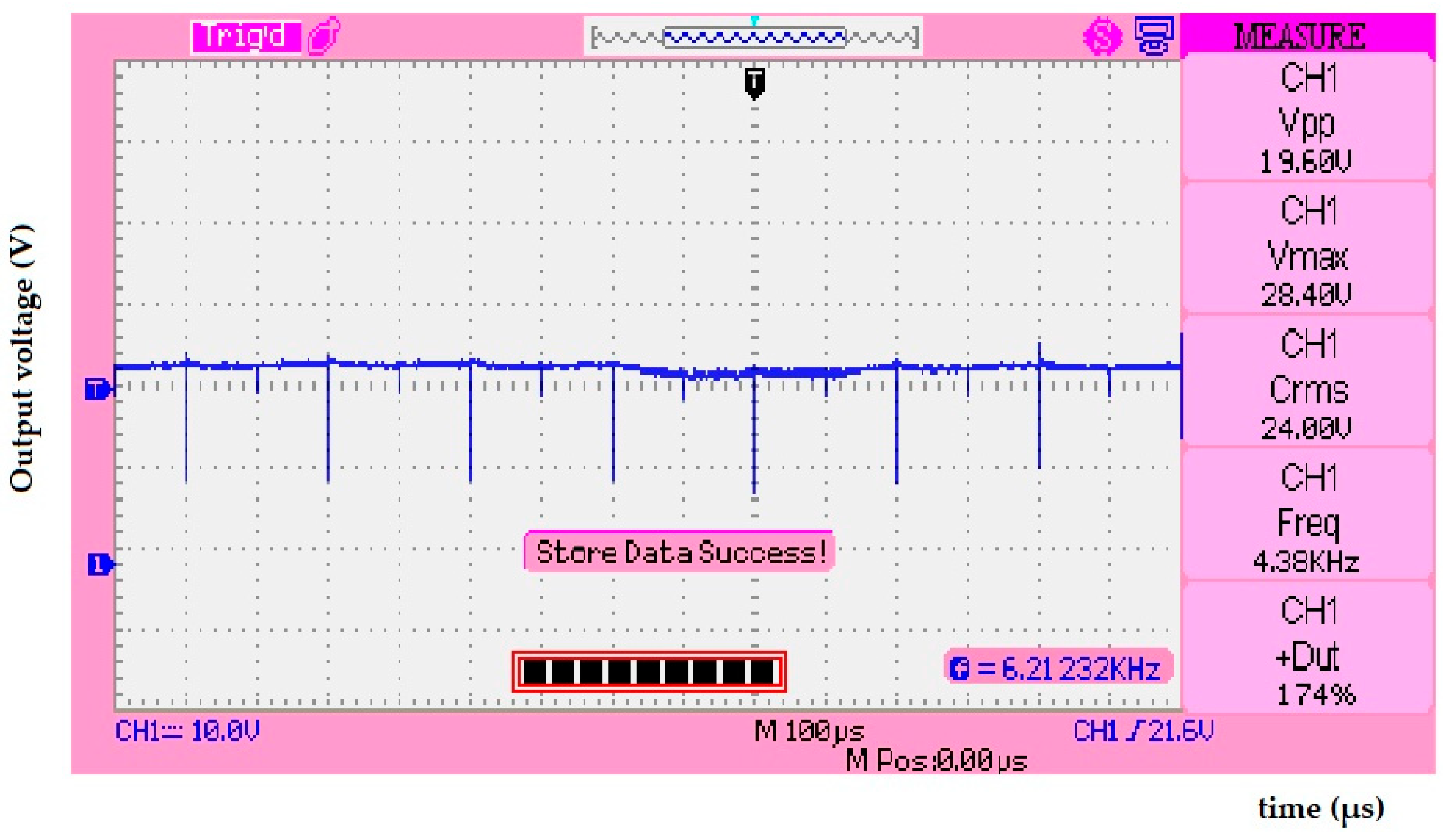
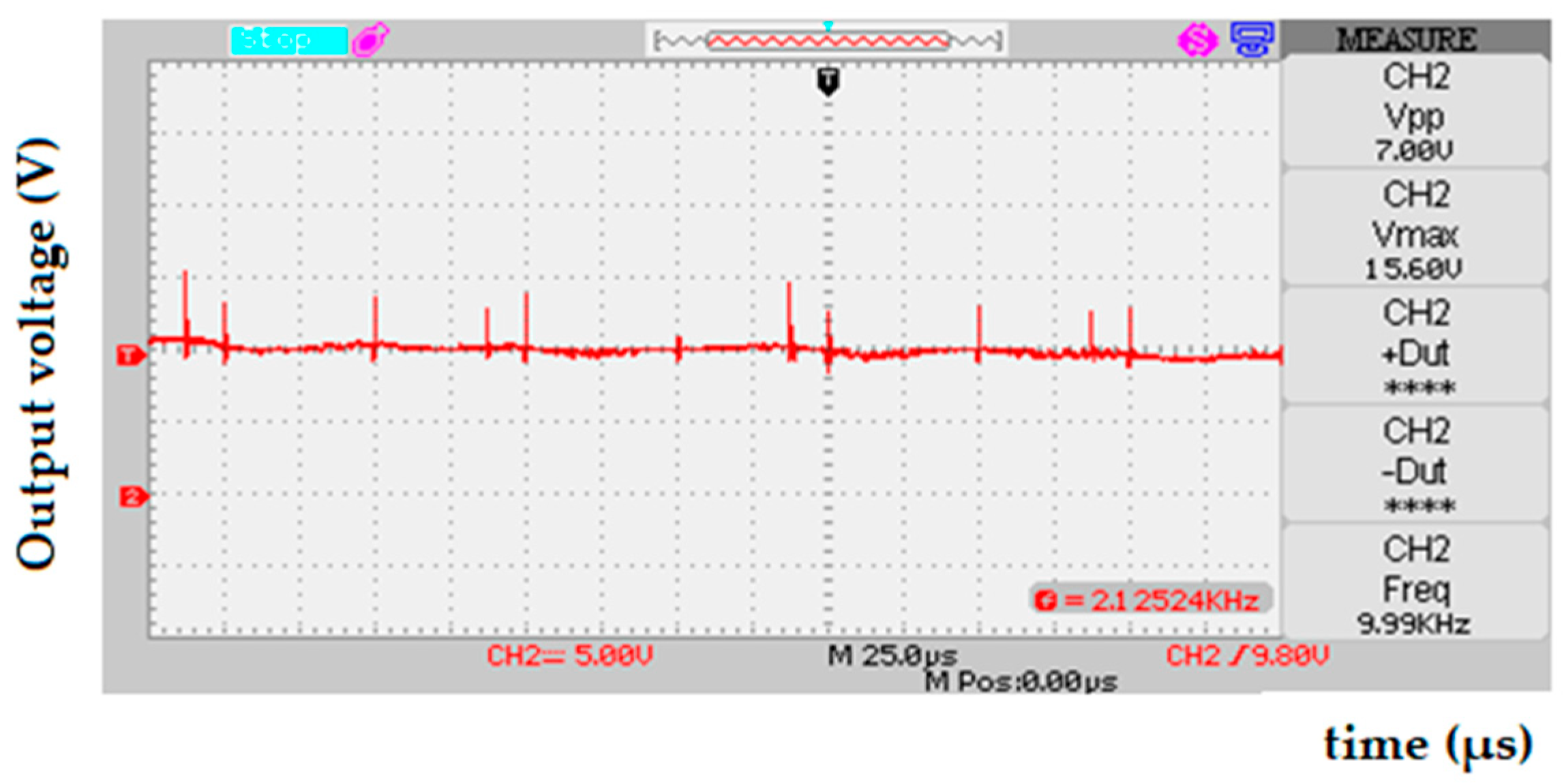
4.1. Two Phase IBC Hardware Results and Discussion
4.2. Six Phase IBC Hardware Results and Discussion
5. Conclusions
Author Contributions
Funding
Institutional Review Board Statement
Informed Consent Statement
Data Availability Statement
Acknowledgments
Conflicts of Interest
Nomenclature
| N | no phase for MPIBC |
| D | duty ratio |
| Vin | input voltage (V) |
| fs | switching frequency (Hz) |
| ∆Iin | input current ripple |
| ∆Vout | output voltage ripple |
| Iout | output current (A) |
| Vout | output voltage (V) |
| LN | inductance at Nth phase (H) |
| CN | capacitance at Nth phase (H) |
| RDS(on) | drain source resistance (Ω) |
| rD | series resistance of diode (Ω) |
| VF | diode forward voltage (V) |
| rL | internal series resistance of the inductor (Ω) |
| rC | internal Series resistance of the capacitor (Ω) |
| Pinput | input power (W) |
| Poutput | output power (W) |
| Pswitch | losses due to switching operation (W) |
| Pdiode | losses due to diode (W) |
| Pinductor | losses due to diode (W) |
| Pinductor | capacitor power loss (W) |
| efficiency |
References
- Chakraborty, S.; Vu, H.N.; Hasan, M.M.; Tran, D.D.; Baghdadi, M.E.; Hegazy, O. DC-DC converter topologies for electric vehicles, plug-in hybrid electric vehicles and fast charging stations: State of the art and future trends. Energies 2019, 12, 1569. [Google Scholar] [CrossRef] [Green Version]
- Elsied, M.; Salem, A.; Oukaour, A.; Gualous, H.; Chaoui, H.; Youssef, F.T.; Belie, D.; Melkebeek, J.; Mohammed, O. Efficient power-electronic converters for electric vehicle applications. In Proceedings of the 2015 IEEE Vehicle Power and Propulsion Conference (VPPC), Montreal, QC, Canada, 19–22 October 2015; pp. 1–6. [Google Scholar]
- Lai, C.M. Development of a novel bidirectional DC/DC converter topology with high voltage conversion ratio for electric vehicles and DC-microgrids. Energies 2016, 9, 410. [Google Scholar] [CrossRef] [Green Version]
- Zahira, R.; Amirtharaj, S.; Selvarani, M.; Lakshmi, D. Design of MOSFET Inverter for a Grid Connected Photovoltaic System. In Proceedings of the AICTE Sponsored National Conference on Recent Advances in On-Board Ship Automation (RAOBSA-2019), Chennai, India, 26–27 September 2019; pp. 253–256. [Google Scholar]
- Guo, J.; Rodriguez, R.; Gareau, J.; Schumacher, D.; Alizadeh, M.; Azer, P.; Bauman, J.; Bilgin, B.; Emadi, A. A Comprehensive Analysis for High-Power Density, High-Efficiency 60 kW Interleaved Boost Converter Design for Electrified Powertrains. IEEE Trans. Veh. Technol. 2020, 69, 7131–7145. [Google Scholar] [CrossRef]
- Sunddararaj, S.P.; Rangarajan, S.S.; Subashini, N.; Subramaniam, U.; Collins, E.R.; Senjyu, T. A novel T-Type Multilevel Inverter for Electric Vehicle and Grid-connected applications. In Proceedings of the 2021 7th International Conference on Electrical Energy Systems (ICEES), Chennai, India, 11–13 February 2021; pp. 166–170. [Google Scholar]
- Subramaniam, U.; Ganesan, S.; Bhaskar, M.S.; Padmanaban, S.; Blaabjerg, F.; Almakhles, D.J. Investigations of AC Microgrid Energy Management Systems Using Distributed Energy Resources and Plug-in Electric Vehicles. Energies 2019, 12, 2834. [Google Scholar] [CrossRef] [Green Version]
- Sunddararaj, S.P.; Rangarajan, S.S.; Subramaniam, U.; Collins, E.R.; Senjyu, T. A new topology of DC-DC Converter with Bidirectional Power Flow Capability Coupled with a Nine Multilevel Inverter for EV Applications. In Proceedings of the 2021 7th International Conference on Electrical Energy Systems (ICEES), Chennai, India, 11–13 February 2021; pp. 177–182. [Google Scholar]
- Dawidziuk, J. Review and comparison of high efficiency high power boost DC/DC converters for photovoltaic applications. Bull. Pol. Acad. Sci. Tech. Sci. 2011, 59, 499–506. [Google Scholar] [CrossRef]
- Wang, L.; Jiao, H.; Yang, G.; Li, J.; Zhang, Y. Current sharing compensation control method for interleaved current source isolated bidirectional DC/DC converters. J. Power Electron. 2022, 22, 1–9. [Google Scholar] [CrossRef]
- Zhang, Z.; Xie, S.; Wu, Z.; Xu, J. Soft-switching and low conduction loss current-fed isolated bidirectional DC–DC converter with PWM plus dual phase-shift control. J. Power Electron. 2020, 20, 664–674. [Google Scholar] [CrossRef]
- Geetha, E.; Maddah, M.; Khosravi, M.M.; Kokabi, A.; Samavatian, V. Dynamic enhancement of interleaved step-up/step-down DC-DC converters using passive damping networks. J. Power Electron. 2020, 20, 657–663. [Google Scholar] [CrossRef]
- Lai, C.M.; Pan, C.T.; Cheng, M.C. High-efficiency modular high step-up interleaved boost converter for DC-microgrid applications. IEEE Trans. Ind. Appl. 2011, 48, 161–171. [Google Scholar] [CrossRef]
- Subramaniam, U.; Palanisamy, K.; Deb, S.; Paul, S.; Bharadwaj, S.C.; Dutta, N. A Solution to Fast Battery Charging Technology With Bi-Directional Series Parallel Resonant Converter LCC In Grid to Vehicle Ambient. In Proceedings of the Innovations in Power and Advanced Computing Technologies (i-PACT), Vellore, India, 22–23 March 2019; pp. 1–6. [Google Scholar]
- Henn, G.A.; Silva, R.N.A.L.; Praca, P.P.; Barreto, L.H.; Oliveira, D.S. Interleaved-boost converter with high voltage gain. IEEE Trans. Power Electron. 2010, 25, 2753–2761. [Google Scholar] [CrossRef]
- Sunddararaj, S.P.; Rangarajan, S.S.; Subramaniam, U.; Collins, E.R.; Senjyu, T. Performance of P/PI/PID Based controller in DC-DC Converter for PV applications and Smart Grid Technology. In Proceedings of the 2021 7th International Conference on Electrical Energy Systems (ICEES), Chennai, India, 11–13 February 2021; pp. 171–176. [Google Scholar]
- Iqbal, A.; Bhaskar, M.S.; Meraj, M.; Padmanaban, S.; Rahman, S. Closed-loop control and boundary for CCM and DCM of nonisolated inverting N× multilevel boost converter for high-voltage step-up applications. IEEE Trans. Ind. Electron. 2019, 67, 2863–2874. [Google Scholar] [CrossRef]
- Abhiram, J.S.; Kumar, S.S.; Jayaprakash, P.; Subramaniam, U. Design and Analysis of a High Step-Up DC-DC Converter Fed Grid Connected Fuel Cell System. In Proceedings of the 2020 International Conference on Power Electronics and Renewable Energy Applications (PEREA), Kannur, India, 27–28 November 2020; pp. 1–6. [Google Scholar]
- Kim, J.H.; Jung, Y.C.; Lee, S.W.; Lee, T.W.; Won, C.Y. Power loss analysis of interleaved soft switching boost converter for single-phase PV-PCS. J. Power Electron. 2010, 10, 335–341. [Google Scholar] [CrossRef]
- Wang, S.; Wang, Y.; Wang, F. Low current ripple high step-up interleaved boost converter with switched-capacitors and switched-inductors. J. Power Electron. 2021, 21, 1646–1658. [Google Scholar] [CrossRef]
- Murali, A.; Wahab, R.S.; Gade, C.S.R.; Annamalai, C.; Subramaniam, U. Assessing Finite Control Set Model Predictive Speed Controlled PMSM Performance for Deployment in Electric Vehicles. World Electr. Veh. J. 2021, 12, 41. [Google Scholar] [CrossRef]
- Meraj, M.; Bhaskar, M.S.; Iqbal, A.; Al-Emadi, N.; Rahman, S. Interleaved multilevel boost converter with minimal voltage multiplier components for high-voltage step-up applications. IEEE Trans. Power Electron. 2020, 35, 12816–12833. [Google Scholar] [CrossRef]
- Ghaffarpour, S.H.; Afjei, S.E.; Salemnia, A. A novel soft-switched interleaved high step-up DC–DC converter for high-efficiency conversion. Int. J. Circuit Theory Appl. 2021, 49, 2515–2532. [Google Scholar] [CrossRef]
- Suresh, S.; Zahira, R. Hardware Implementation of Two Stage Interleaved Boost Converter for Electric Vehicle Application. Int. J. Veh. Struct. Syst. 2021, 13, 373–377. [Google Scholar] [CrossRef]
- Lipu, M.S.H.; Faisal, M.; Ansari, S.; Hannan, M.A.; Karim, T.F.; Ayob, A.; Hussain, A.; Miah, M.; Saad, M.H.M. Review of Electric Vehicle Converter Configurations, Control Schemes and Optimizations: Challenges and Suggestions. Electronics 2021, 10, 477. [Google Scholar] [CrossRef]
- Zhang, Y.; Liu, Q.; Li, J.; Sumner, M. A common ground switched Quasi- Z –Source Bidirectional DC-DC Converter with wide voltage –Gain range for EVs with Hybrid Energy Sources. IEEE Trans. Ind. Electron. 2017, 65, 5188–5200. [Google Scholar] [CrossRef]
- Zhao, C.; Round, S.D.; Kolar, J.W. An isolated three- port bidirectional DC-DC converter with decoupled with power flow management. IEEE Trans. Power Electron. 2018, 23, 2443–2453. [Google Scholar] [CrossRef]
- Maalandish, M.; Hosseini, S.H.; Ghasemzadeh, S.; Babaei, E.; Alishah, R.S.; Jalilzadeh, T. Six-phase interleaved boost dc/dc converter with high-voltage gain and reduced voltage stress. IET Power Electron. 2017, 10, 1904–1914. [Google Scholar] [CrossRef]


| DC-DC Converter | Ripple (Voltage/Current) | Switching Frequency | Complicity of Control Circuit | High Power Conversion | Cost |
|---|---|---|---|---|---|
| IBC [1] | Reasonable | High | Reasonable | Suitable | Low |
| QZBC [26] | Simple | High | Multifaceted | Suitable | Medium |
| MPIC [27] | Multifaceted | Low | Multifaceted | Suitable | High |
| MPIBC | Simple | Low | Reasonable | Suitable | Medium |
| DC-DC Converter | Objective | Outcomes | Benefits |
|---|---|---|---|
| IBC [1] |
|
|
|
| QZBC [26] |
|
|
|
| MPIC [27] |
|
|
|
| MPIBC |
|
|
|
| Parameter | Value | Unit |
|---|---|---|
| Solar PV voltage | 20 | V |
| Output voltage | 40 | V |
| Output current | 1.25 | A |
| Output power | 50 | W |
| L1 = L2 = L (2 phase IBC) | 3.225 m | H |
| L1 = L2 = L3 = L (3 phase IBC) | 2.15 m | H |
| L1 = L2 = L3 = L4 = L (4 phase IBC) | 1.613 m | H |
| L1 = L2 = L3 = L4 = L5 = L6 = L (6 phase IBC) | 1.075 m | H |
| C (2 phase IBC) | 504 µ | F |
| C (3 phase IBC) | 336 µ | F |
| C (4 phase IBC) | 252 µ | F |
| C (6 phase IBC) | 168 µ | F |
| Rload | 32 | Ω |
| Lload | 120 m | H |
| Switching frequency (fs) | 31 k | Hz |
| Input Current Ripple (∆Iin) | 5% | - |
| Output Voltage Ripple (∆Vout) | 2% | - |
| Duty ratio (D) | 50% | - |
| Drain Source Resistance (RDS(on)) | 0.045 | Ω |
| Series resistance of Diode (rD) | 0.30 | Ω |
| Internal Series resistance of the inductor (rL) | 0.25 | Ω |
| Internal Series resistance of the capacitor (rC) | 0.05 | Ω |
| Equation | Equation Meaning | Equation Number |
|---|---|---|
| Switching loss | (4) | |
| Diode loss | (5) | |
| Inductor loass | (6) | |
| Capactior loss | (7) | |
| Input power | (8) | |
| Efficiency | (9) |
| Number of Phases of MPIBC | Output Voltage (Vout) in V | Output Current (Iout) in A | Output Power (Po) in W |
|---|---|---|---|
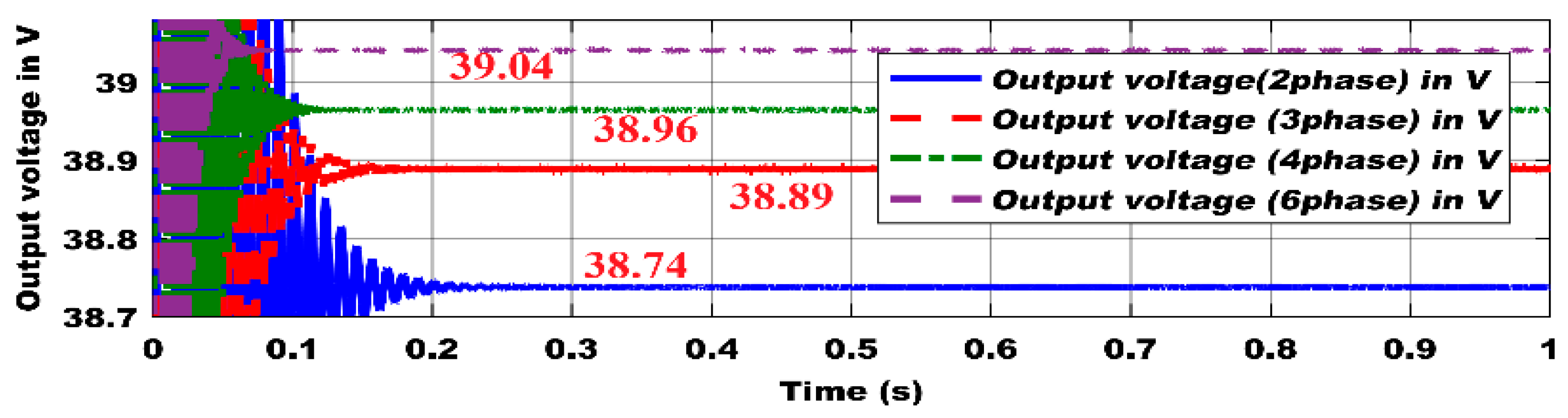
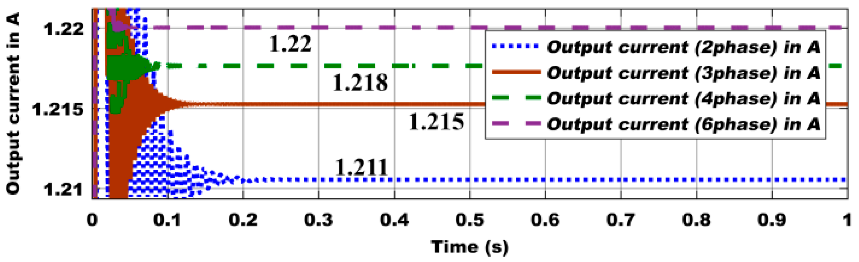
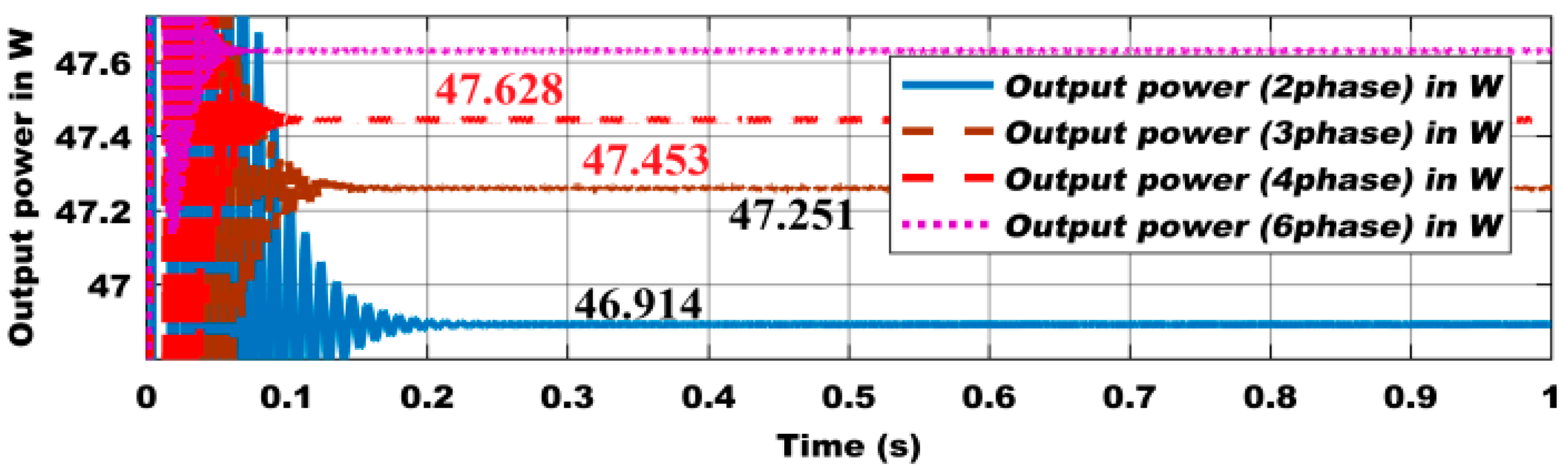
| 2 | 38.74 | 1.211 | 46.914 |
| 3 | 38.89 | 1.215 | 47.251 |
| 4 | 38.96 | 1.218 | 47.453 |
| 6 | 39.04 | 1.220 | 47.628 |
| Number of Phases of MPIBC | Output Voltage (Vout) in V | Output Current (Iout) in A | Output Power (Po) in kW |
|---|---|---|---|
| 2 | 434 | 13.56 | 5.887 |
| 3 | 435.7 | 13.62 | 5.933 |
| 4 | 436.6 | 13.64 | 5.956 |
| 6 | 437.4 | 13.67 | 5.979 |
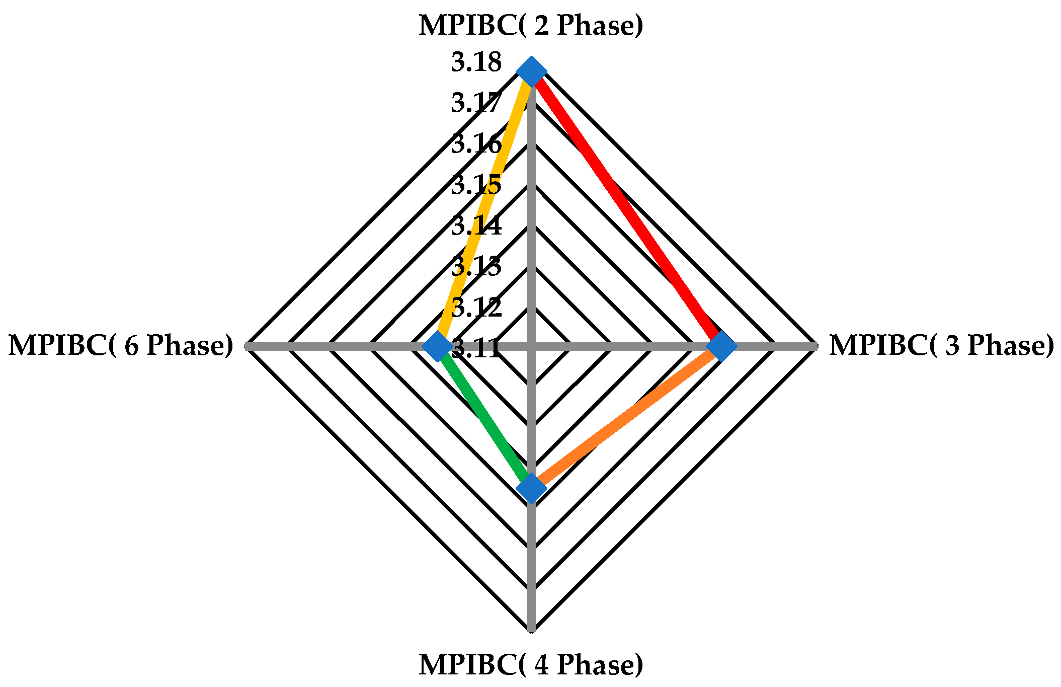
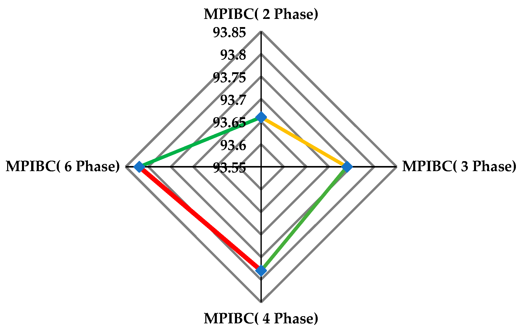
| Number of Phases of MPIBC | Ploss (W) | Pinput (W) | Poutput (W) | %Efficiency |
|---|---|---|---|---|
| 2 | 3.1772 | 50.1772 | 46.914 | 93.66 |
| 3 | 3.1565 | 50.1565 | 47.251 | 93.74 |
| 4 | 3.1448 | 50.1448 | 47.453 | 93.78 |
| 6 | 3.1330 | 50.1330 | 47.628 | 93.82 |
| Number of Phases of MPIBC | Ploss (W) | Pinput (kW) | Poutput (kW) | %Efficiency |
|---|---|---|---|---|
| 2 | 267.347 | 6.154 | 5.887 | 95.66 |
| 3 | 266.880 | 6.199 | 5.933 | 95.71 |
| 4 | 266.263 | 6.222 | 5.956 | 95.72 |
| 6 | 266.010 | 6.245 | 5.979 | 95.74 |
| Parameters | BC [1] | IBC [1] | MPIBC |
|---|---|---|---|
| Input Voltage (V) | 200 | 200 | 200 |
| Output Voltage (V) | 400 | 400 | 500 |
| Number of Phase | 1 | 4 | 6 |
| Output Power (kW) | 30 | 30 | 34.38 |
| Switching Freqency (kHz) | 20 | 20 | 20 |
| Inductor Current (A) | 250 | 250 | 182.7 |
| Inductor (µH) | 400 | 100 | 66.67 |
| Capactior (µF) | 780 | 195 | 168 |
| Duty Cycle | 0.5 | 0.5 | 0.5 |
| Inductor Current Ripple (A) | 12.5 | 12.5 | 9.28 |
| Parameters | Six Phase IBC [28] | Six Phase MPIBC |
|---|---|---|
| Input Voltage (V) | 24 | 24 |
| Number of Phase | 6 | 6 |
| Switching Freqency (kHz) | 25 | 25 |
| Duty Cycle | 0.6 | 0.6 |
| Output Voltage (V) | 207 | 213.8 |
| Output Power (W) | 453 | 487.6 |
| %Efficiency | 96.90 | 98.68 |
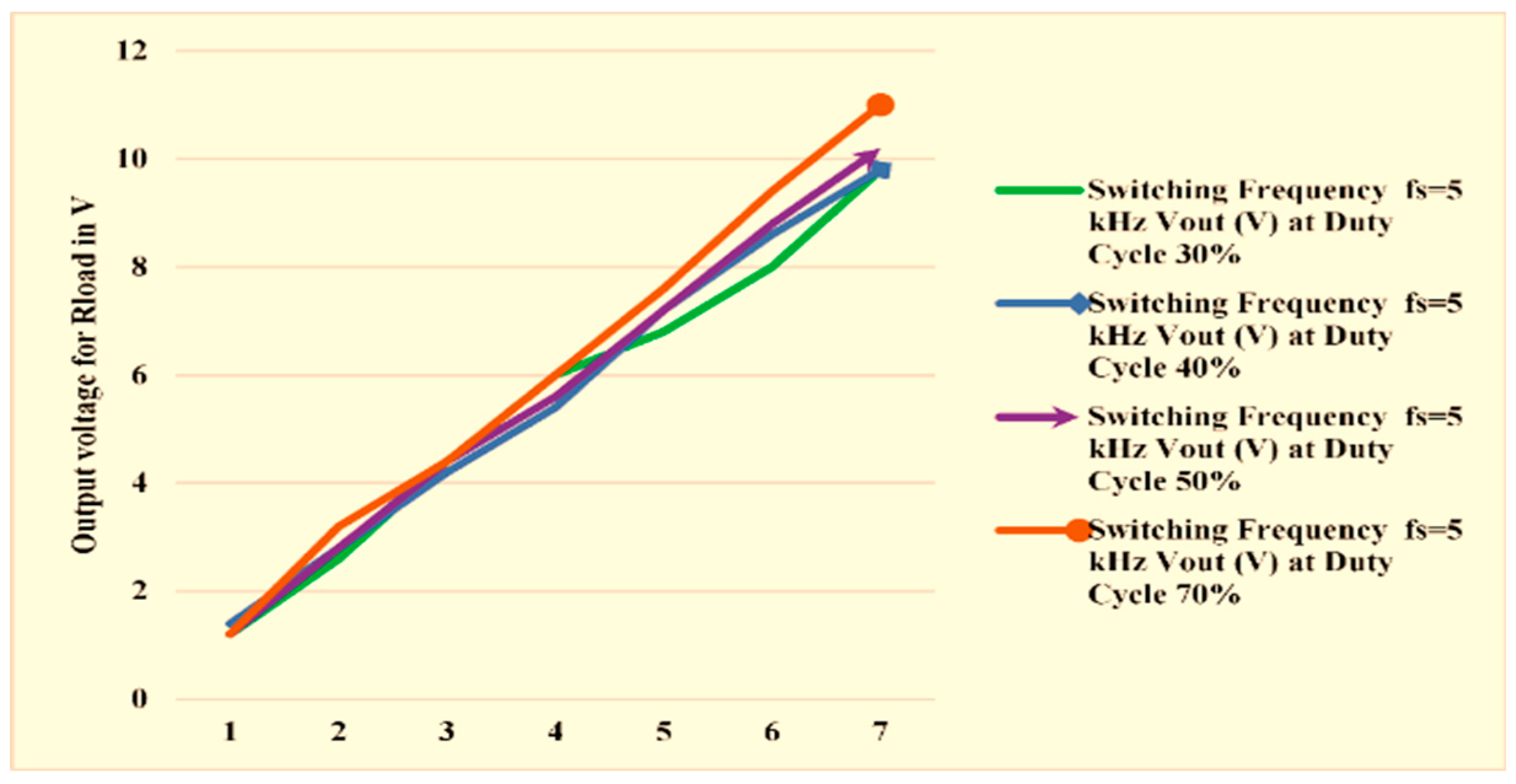
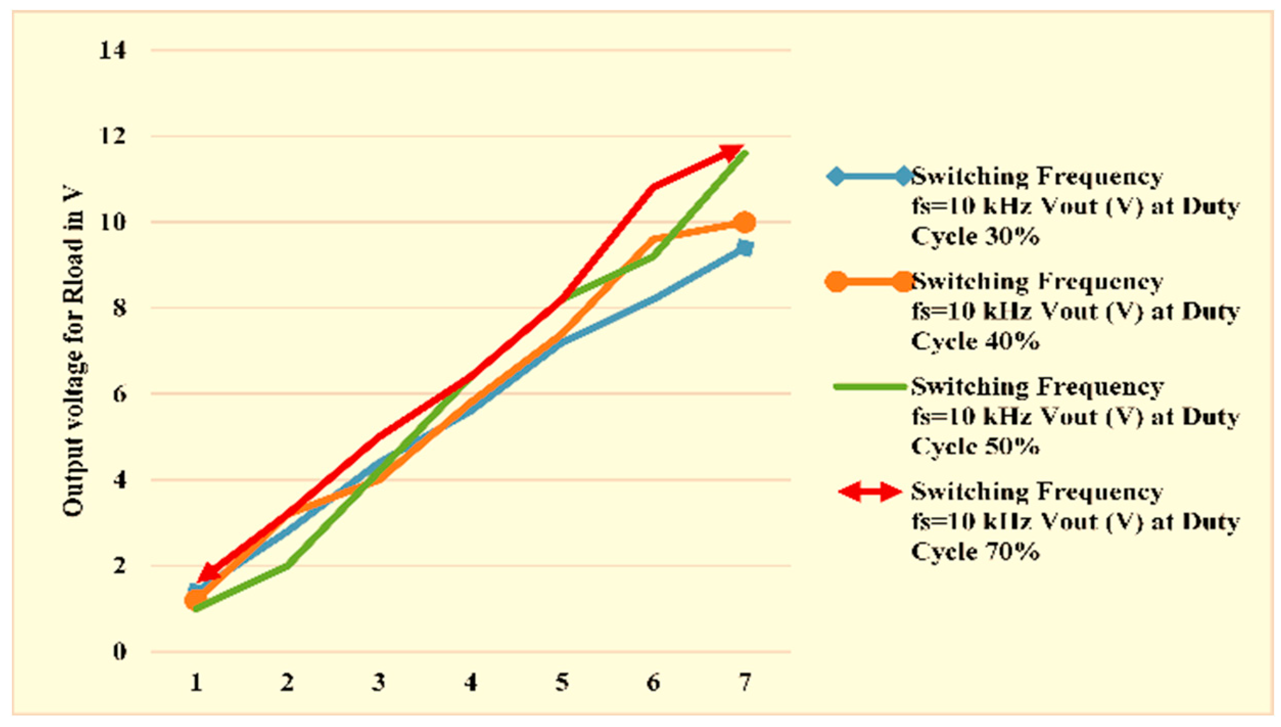
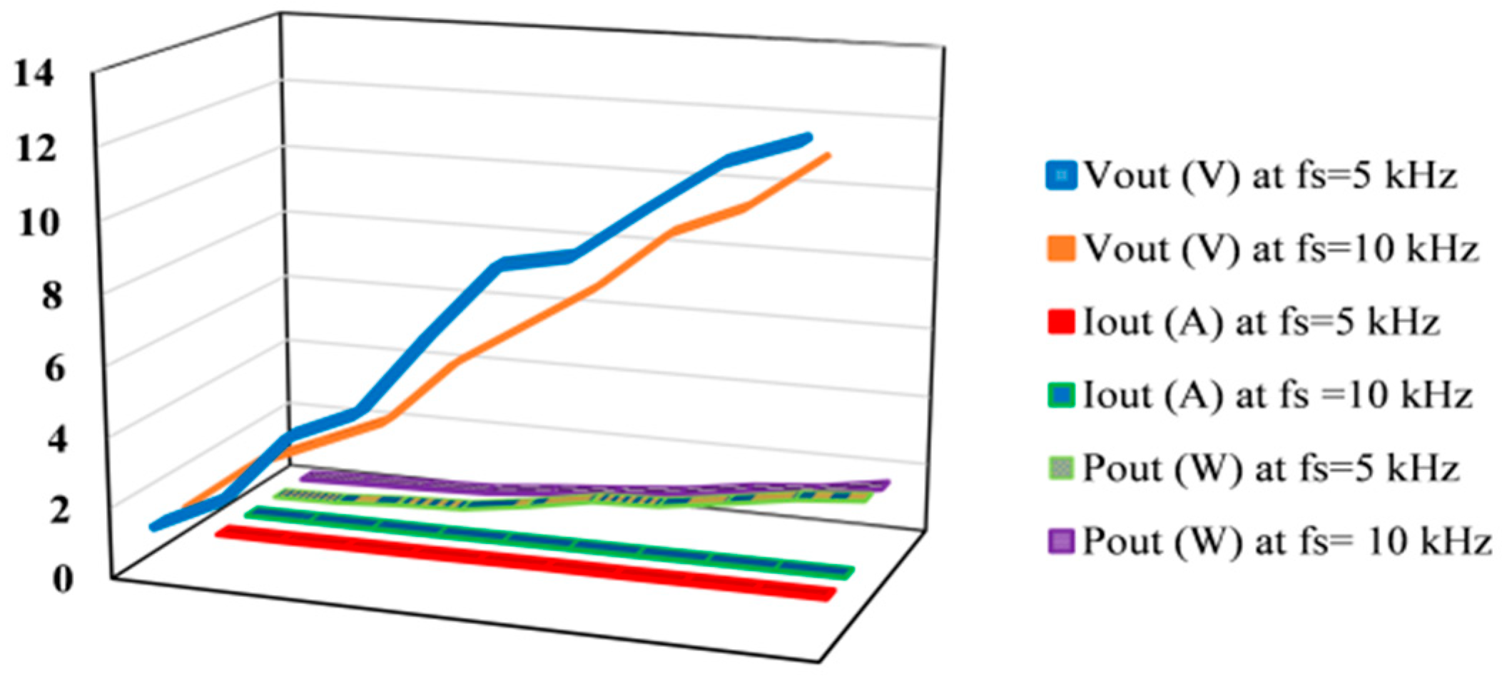
| Vin (V) | Switching Frequency fs = 5 kHz | Switching Frequency fs = 10 kHz | ||||||
|---|---|---|---|---|---|---|---|---|
| Vout (V) at D = 0.3 | Vout (V) at D = 0.4 | Vout (V) at D = 0.5 | Vout (V) at D = 0.7 | Vout (V) at D = 0.3 | Vout (V) at D = 0.4 | Vout (V) at D = 0.5 | Vout (V) at D = 0.7 | |
| 0.5 | 1.2 | 1.4 | 1.2 | 1.2 | 1.4 | 1.2 | 1 | 1.6 |
| 1 | 2.6 | 2.8 | 2.8 | 3.2 | 2.8 | 3.2 | 2 | 3.2 |
| 1.5 | 4.4 | 4.2 | 4.4 | 4.4 | 4.4 | 4 | 4.2 | 5 |
| 2 | 6 | 5.4 | 5.6 | 6 | 5.6 | 5.8 | 6.4 | 6.4 |
| 2.5 | 6.8 | 7.2 | 7.2 | 7.6 | 7.2 | 7.4 | 8.2 | 8.2 |
| 3 | 8 | 8.6 | 8.8 | 9.4 | 8.2 | 9.6 | 9.2 | 10.8 |
| 3.5 | 9.8 | 9.8 | 10.2 | 11 | 9.4 | 10 | 11.6 | 11.8 |
| Vin (V) | Switching Frequency fs = 5 kHz | Switching Frequency fs = 10 kHz | ||||
|---|---|---|---|---|---|---|
| Vout (V) | Iout (mA) | Pout (mW) | Vout (V) | Iout (mA) | Pout (mW) | |
| 0.5 | 1.4 | 14 | 19.6 | 1.4 | 14 | 19.6 |
| 1.1 | 2.3 | 23 | 52.9 | 2.8 | 28 | 78.4 |
| 1.5 | 4.3 | 43 | 184.9 | 3.6 | 36 | 129.6 |
| 2 | 5.12 | 51.2 | 262.14 | 4.4 | 44 | 193.6 |
| 2.5 | 7.38 | 73.8 | 544.64 | 6.2 | 62 | 384.4 |
| 3 | 9.46 | 94.6 | 894.92 | 7.4 | 74 | 547.6 |
| 3.5 | 9.83 | 98.3 | 966.29 | 8.6 | 86 | 739.6 |
| 4 | 11.22 | 112.2 | 1258.88 | 10.2 | 102 | 1040.4 |
| 4.5 | 12.54 | 125.4 | 1572.52 | 11 | 110 | 1210 |
| 5 | 13.2 | 132 | 1742.4 | 12.4 | 124 | 1537.6 |
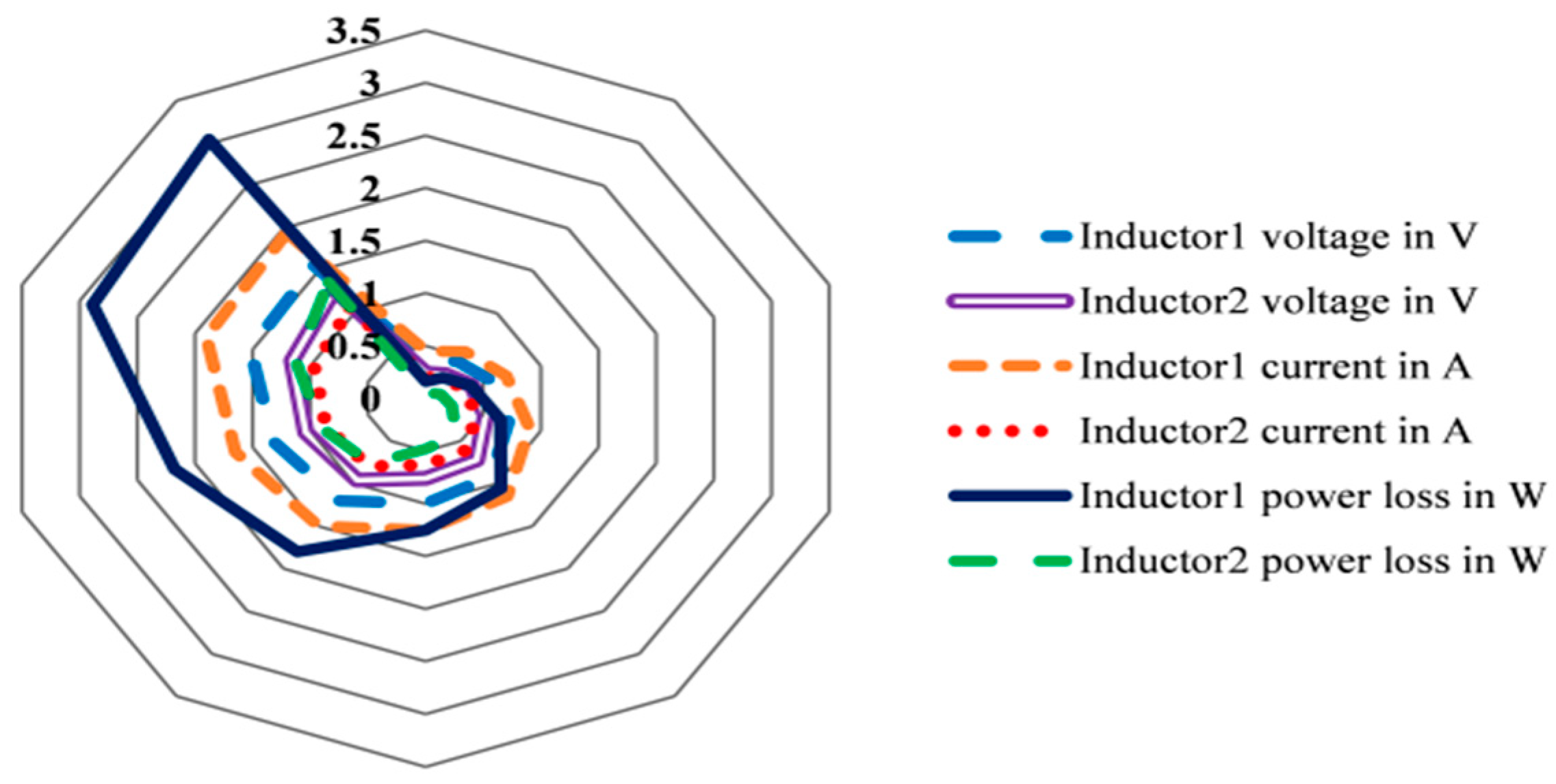
| Inductor1 Voltage (V) | Inductor2 Voltage (V) | IL1 (A) | IL2 (A) | PL1 (W) | PL2 (W) |
|---|---|---|---|---|---|
| 0.28 | 0.28 | 0.35 | 0.23 | 0.098 | 0.065 |
| 0.36 | 0.36 | 0.45 | 0.30 | 0.162 | 0.108 |
| 0.72 | 0.56 | 0.9 | 0.47 | 0.648 | 0.261 |
| 0.76 | 0.68 | 0.95 | 0.57 | 0.722 | 0.385 |
| 0.96 | 0.84 | 1.2 | 0.70 | 1.152 | 0.588 |
| 1.16 | 1.04 | 1.45 | 0.87 | 1.682 | 0.901 |
| 1.32 | 1.2 | 1.65 | 1.00 | 2.178 | 1.200 |
| 1.44 | 1.28 | 1.8 | 1.07 | 2.592 | 1.365 |
| 1.56 | 1.48 | 1.95 | 1.23 | 3.042 | 1.825 |
| 1.64 | 1.64 | 2.05 | 1.37 | 3.362 | 2.241 |
| Inductor1 voltage (V) | Inductor2 voltage (V) | IL1 (A) | IL2 (A) | PL1 (W) | PL2 (W) |
|---|---|---|---|---|---|
| 0.360 | 0.240 | 0.450 | 0.200 | 0.162 | 0.048 |
| 0.440 | 0.280 | 0.550 | 0.233 | 0.242 | 0.065 |
| 0.560 | 0.400 | 0.700 | 0.333 | 0.392 | 0.133 |
| 0.720 | 0.520 | 0.900 | 0.433 | 0.648 | 0.225 |
| 0.920 | 0.720 | 1.150 | 0.600 | 1.058 | 0.432 |
| 1.000 | 0.760 | 1.250 | 0.633 | 1.250 | 0.481 |
| 1.200 | 0.960 | 1.500 | 0.800 | 1.800 | 0.768 |
| 1.320 | 1.040 | 1.650 | 0.867 | 2.178 | 0.901 |
| 1.520 | 1.160 | 1.900 | 0.967 | 2.888 | 1.121 |
| 1.560 | 1.280 | 1.950 | 1.067 | 3.042 | 1.365 |
| Vin (V) | Switching Frequency fs = 5 kHz | ||
|---|---|---|---|
| Vout (V) | Iout (mA) | Pout (W) | |
| 0.5 | 11 | 110 | 1.21 |
| 1.0 | 11.6 | 116 | 1.34 |
| 1.5 | 11.8 | 118 | 1.39 |
| 2 | 12.1 | 121 | 1.46 |
| 2.5 | 12.4 | 124 | 1.53 |
| 3 | 12.8 | 128 | 1.64 |
| 3.5 | 13.1 | 131 | 1.72 |
| 4 | 13.6 | 136 | 1.85 |
| 4.5 | 14 | 140 | 1.96 |
| 5 | 15.6 | 156 | 2.43 |
Publisher’s Note: MDPI stays neutral with regard to jurisdictional claims in published maps and institutional affiliations. |
© 2022 by the authors. Licensee MDPI, Basel, Switzerland. This article is an open access article distributed under the terms and conditions of the Creative Commons Attribution (CC BY) license (https://creativecommons.org/licenses/by/4.0/).
Share and Cite
Sampath, S.; Rahiman, Z.; Chenniappan, S.; Sundaram, E.; Subramaniam, U.; Padmanaban, S. Efficient Multi-Phase Converter for E-Mobility. World Electr. Veh. J. 2022, 13, 67. https://doi.org/10.3390/wevj13040067
Sampath S, Rahiman Z, Chenniappan S, Sundaram E, Subramaniam U, Padmanaban S. Efficient Multi-Phase Converter for E-Mobility. World Electric Vehicle Journal. 2022; 13(4):67. https://doi.org/10.3390/wevj13040067
Chicago/Turabian StyleSampath, Suresh, Zahira Rahiman, Sharmeela Chenniappan, Elango Sundaram, Umashankar Subramaniam, and Sanjeevikumar Padmanaban. 2022. "Efficient Multi-Phase Converter for E-Mobility" World Electric Vehicle Journal 13, no. 4: 67. https://doi.org/10.3390/wevj13040067