
Exploiting the Acceleration Voltage Dependence of EMCD

 , , and
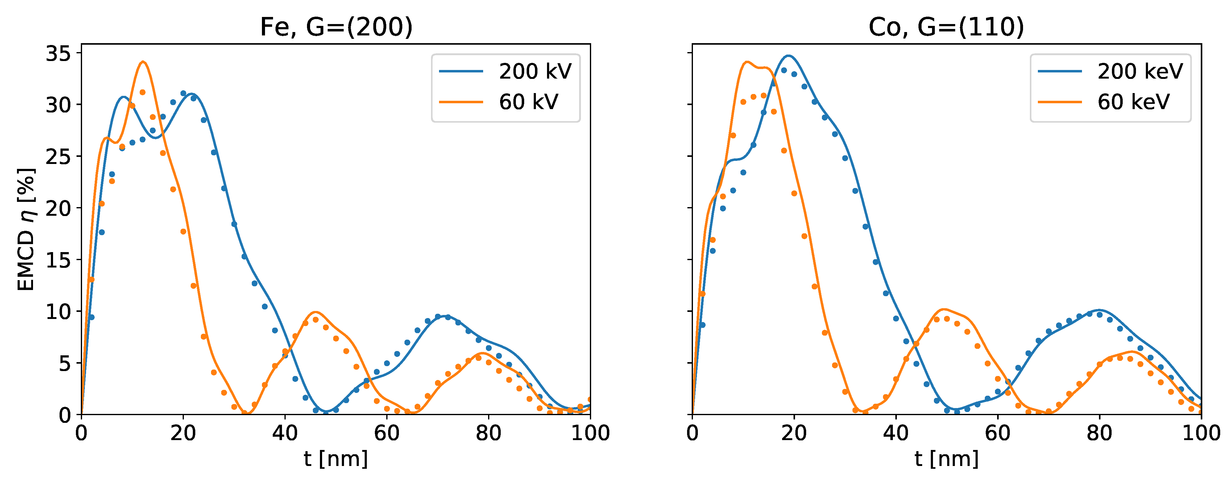
Abstract
:1. Introduction
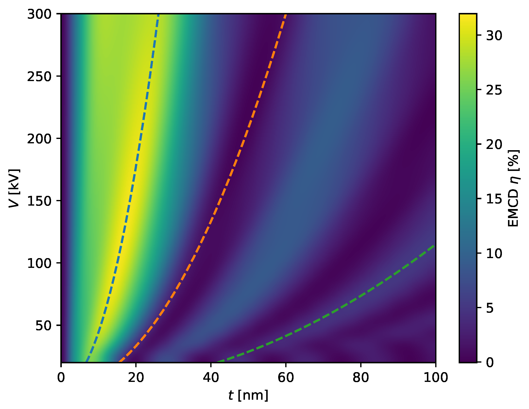
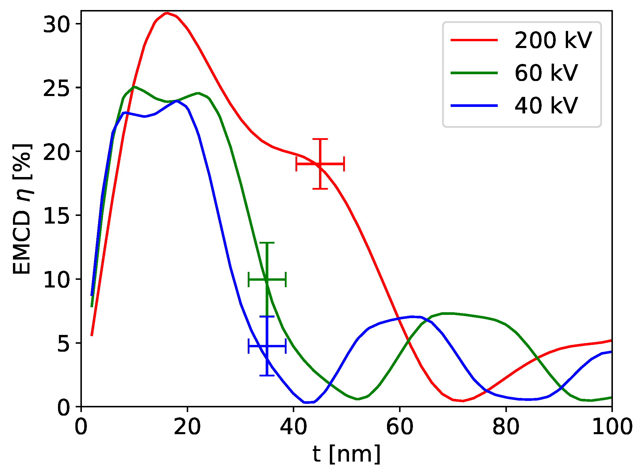
2. Results
2.1. Theory
- We limit the derivation to an incident three-beam and outgoing two-beam case in the zero-order Laue zone of a sample that is single-crystalline in the probed region with a centro-symmetric crystal structure;
- We assume that the sample is a slab of thickness t with an entrance and an exit plane essentially perpendicular to the beam propagation axis;
- We assume that the inelastic scattering process is at least four-fold rotationally symmetric around the optical axis and that the characteristic momentum transfer is much smaller than the chosen reciprocal lattice distance . This implies that the inelastic scattering in the chosen geometry is only dependent on the scattering atom’s spin-state, but not influenced significantly by any anisotropic crystal field;
- We assume that the atoms of the investigated species are homogeneously distributed along the beam propagation axis and that for all atom positions and the chosen lattice vector .
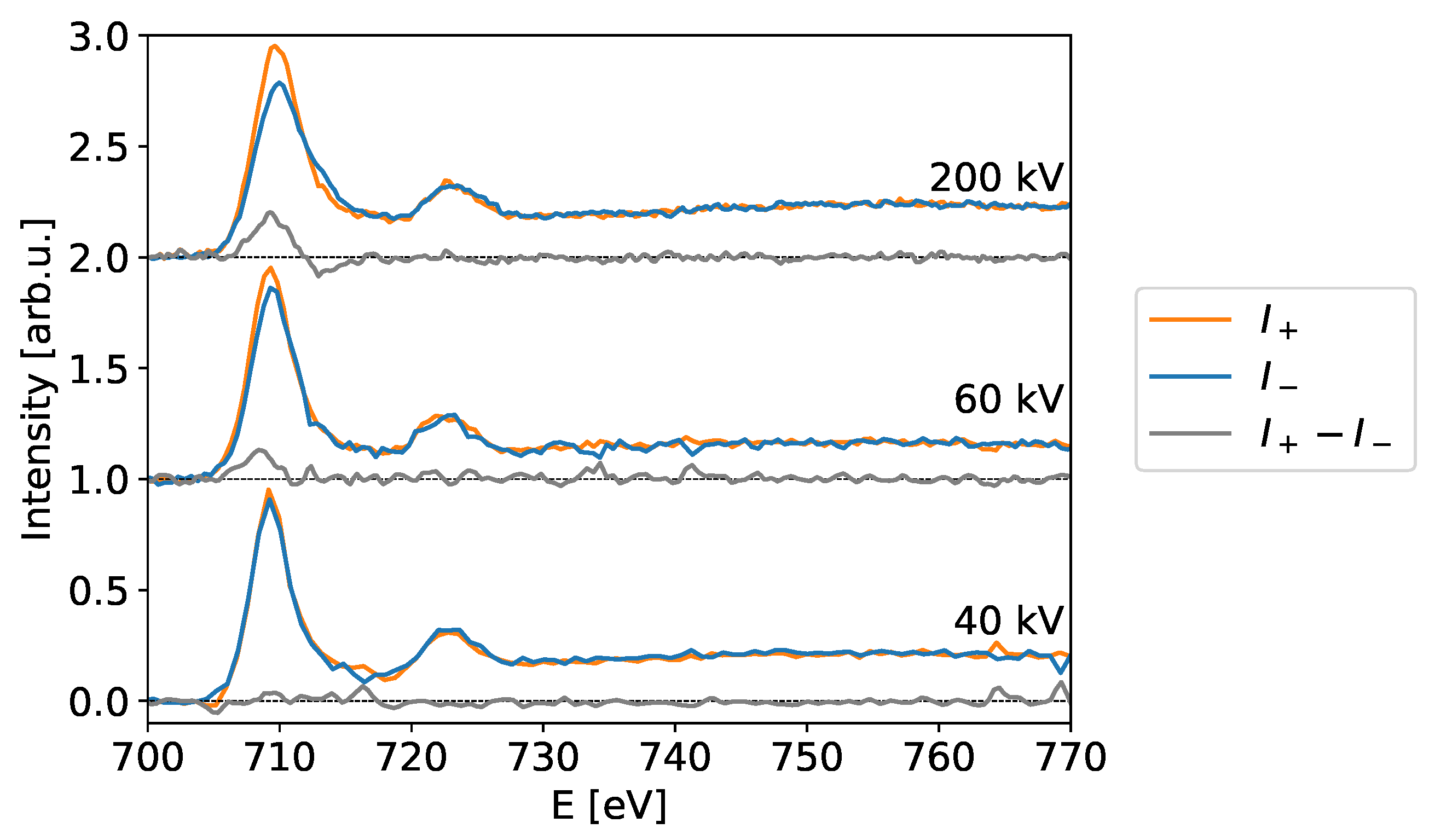
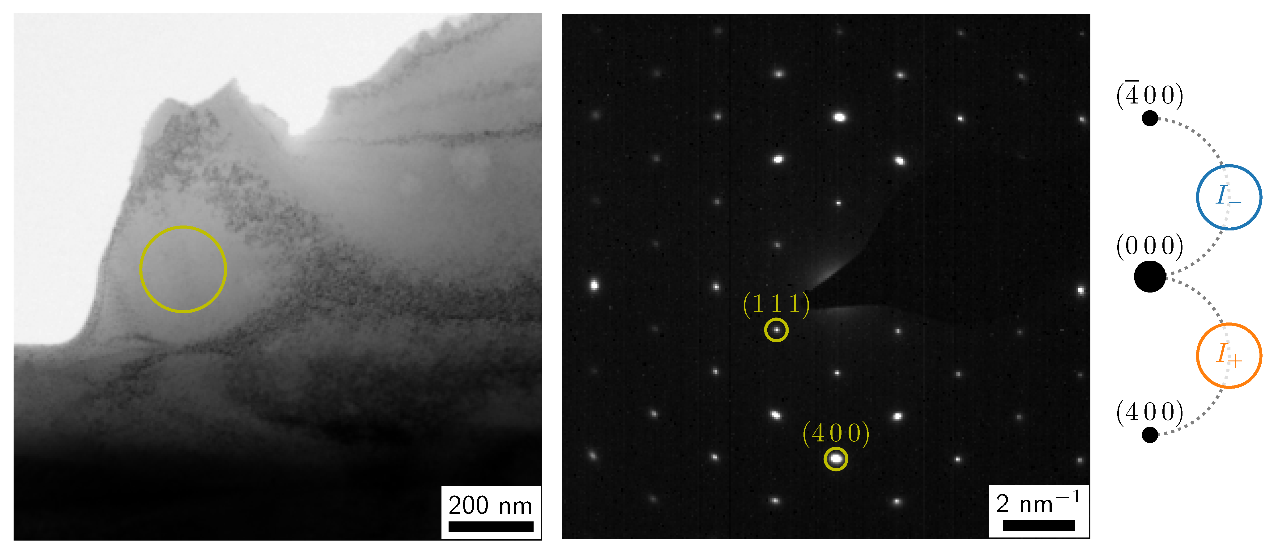
2.2. Experiments
3. Discussion
4. Materials and Methods
5. Conclusions
Author Contributions
Funding
Institutional Review Board Statement
Informed Consent Statement
Data Availability Statement
Conflicts of Interest
Abbreviations
| DDSCS | Double-differential scattering cross-Section |
| EMCD | Energy-loss magnetic chiral dichroism |
| EELS | Electron energy-loss spectrometry |
| MDFF | Mixed dynamic form factor |
| TEM | Transmission electron microscopy |
| XAS | X-ray absorption spectroscopy |
| XMCD | X-ray magnetic circular dichroism |
Appendix A. Derivation of the EMCD Effect
References
- Botton, G. A new approach to study bonding anisotropy with EELS. J. Electron Spectrosc. Relat. Phenom. 2005, 143, 129–137. [Google Scholar] [CrossRef]
- Schattschneider, P.; Hébert, C.; Franco, H.; Jouffrey, B. Anisotropic relativistic cross sections for inelastic electron scattering, and the magic angle. Phys. Rev. B 2005, 72, 045142. [Google Scholar] [CrossRef] [Green Version]
- Hébert, C.; Schattschneider, P. A proposal for dichroic experiments in the electron microscope. Ultramicroscopy 2003, 96, 463–468. [Google Scholar] [CrossRef]
- Schattschneider, P.; Jouffrey, B. Channeling, localization and the density matrix in inelastic electron scattering. Ultramicroscopy 2003, 96, 453–462. [Google Scholar] [CrossRef]
- Schattschneider, P.; Werner, W. Coherence in electron energy loss spectrometry. J. Electron Spectrosc. Relat. Phenom. 2005, 143, 81–95. [Google Scholar] [CrossRef]
- CHIRALTEM. Available online: https://cordis.europa.eu/project/id/508971 (accessed on 9 February 2021).
- Schattschneider, P.; Rubino, S.; Hebert, C.; Rusz, J.; Kunes, J.; Novák, P.; Carlino, E.; Fabrizioli, M.; Panaccione, G.; Rossi, G. Detection of magnetic circular dichroism using a transmission electron microscope. Nature 2006, 441, 486–488. [Google Scholar] [CrossRef]
- Rusz, J.; Rubino, S.; Schattschneider, P. First-principles theory of chiral dichroism in electron microscopy applied to 3d ferromagnets. Phys. Rev. B 2007, 75, 214425. [Google Scholar] [CrossRef] [Green Version]
- Hébert, C.; Schattschneider, P.; Rubino, S.; Novak, P.; Rusz, J.; Stöger-Pollach, M. Magnetic circular dichroism in electron energy loss spectrometry. Ultramicroscopy 2008, 108, 277–284. [Google Scholar] [CrossRef]
- Verbeeck, J.; Hébert, C.; Rubino, S.; Novák, P.; Rusz, J.; Houdellier, F.; Gatel, C.; Schattschneider, P. Optimal aperture sizes and positions for EMCD experiments. Ultramicroscopy 2008, 108, 865–872. [Google Scholar] [CrossRef] [PubMed]
- Löffler, S.; Schattschneider, P. A software package for the simulation of energy-loss magnetic chiral dichroism. Ultramicroscopy 2010, 110, 831–835. [Google Scholar] [CrossRef] [PubMed]
- Rusz, J. Modified automatic term selection v2: A faster algorithm to calculate inelastic scattering cross-sections. Ultramicroscopy 2017, 177, 20–25. [Google Scholar] [CrossRef]
- Schattschneider, P.; Stöger-Pollach, M.; Rubino, S.; Sperl, M.; Hurm, C.; Zweck, J.; Rusz, J. Detection of magnetic circular dichroism on the two-nanometer scale. Phys. Rev. B 2008, 78, 104413. [Google Scholar] [CrossRef]
- Schneider, S.; Pohl, D.; Löffler, S.; Rusz, J.; Kasinathan, D.; Schattschneider, P.; Schultz, L.; Rellinghaus, B. Magnetic properties of single nanomagnets: Electron energy-loss magnetic chiral dichroism on FePt nanoparticles. Ultramicroscopy 2016, 171, 186–194. [Google Scholar] [CrossRef] [Green Version]
- Verbeeck, J.; Schattschneider, P.; Lazar, S.; Stöger-Pollach, M.; Löffler, S.; Steiger-Thirsfeld, A.; Van Tendeloo, G. Atomic scale electron vortices for nanoresearch. Appl. Phys. Lett. 2011, 99, 203109. [Google Scholar] [CrossRef] [Green Version]
- Schattschneider, P.; Schaffer, B.; Ennen, I.; Verbeeck, J. Mapping spin-polarized transitions with atomic resolution. Phys. Rev. B 2012, 85, 134422. [Google Scholar] [CrossRef] [Green Version]
- Schachinger, T.; Löffler, S.; Steiger-Thirsfeld, A.; Stöger-Pollach, M.; Schneider, S.; Pohl, D.; Rellinghaus, B.; Schattschneider, P. EMCD with an electron vortex filter: Limitations and possibilities. Ultramicroscopy 2017, 179, 15–23. [Google Scholar] [CrossRef] [Green Version]
- Rusz, J.; Muto, S.; Spiegelberg, J.; Adam, R.; Tatsumi, K.; Bürgler, D.E.; Oppeneer, P.M.; Schneider, C.M. Magnetic measurements with atomic-plane resolution. Nat. Commun. 2016, 7, 12672. [Google Scholar] [CrossRef]
- Warot-Fonrose, B.; Houdellier, F.; Hÿtch, M.; Calmels, L.; Serin, V.; Snoeck, E. Mapping inelastic intensities in diffraction patterns of magnetic samples using the energy spectrum imaging technique. Ultramicroscopy 2008, 108, 393–398. [Google Scholar] [CrossRef]
- Salafranca, J.; Gazquez, J.; Pérez, N.; Labarta, A.; Pantelides, S.T.; Pennycook, S.J.; Batlle, X.; Varela, M. Surfactant Organic Molecules Restore Magnetism in Metal-Oxide Nanoparticle Surfaces. Nano Lett. 2012, 12, 2499–2503. [Google Scholar] [CrossRef]
- Thersleff, T.; Rusz, J.; Rubino, S.; Hjörvarsson, B.; Ito, Y.; Zaluzec, N.J.; Leifer, K. Quantitative analysis of magnetic spin and orbital moments from an oxidized iron (1 1 0) surface using electron magnetic circular dichroism. Sci. Rep. 2015, 5, 13012. [Google Scholar] [CrossRef] [Green Version]
- Song, D.; Ma, L.; Zhou, S.; Zhu, J. Oxygen deficiency induced deterioration in microstructure and magnetic properties at Y3Fe5O12/Pt interface. Appl. Phys. Lett. 2015, 107, 042401. [Google Scholar] [CrossRef]
- Wang, Z.; Tavabi, A.H.; Jin, L.; Rusz, J.; Tyutyunnikov, D.; Jiang, H.; Moritomo, Y.; Mayer, J.; Dunin-Borkowski, R.E.; Yu, R.; et al. Atomic scale imaging of magnetic circular dichroism by achromatic electron microscopy. Nat. Mater. 2018, 17, 221–225. [Google Scholar] [CrossRef]
- Wang, Z.; Zhong, X.; Yu, R.; Cheng, Z.; Zhu, J. Quantitative experimental determination of site-specific magnetic structures by transmitted electrons. Nat. Commun. 2013, 4, 1395. [Google Scholar] [CrossRef] [Green Version]
- Ennen, I.; Löffler, S.; Kübel, C.; Wang, D.; Auge, A.; Hütten, A.; Schattschneider, P. Site-specific chirality in magnetic transitions. J. Magn. Magn. Mater. 2012, 324, 2723–2726. [Google Scholar] [CrossRef]
- Loukya, B.; Negi, D.S.; Dileep, K.; Pachauri, N.; Gupta, A.; Datta, R. Effect of Bloch wave electron propagation and momentum-resolved signal detection on the quantitative and site-specific electron magnetic chiral dichroism of magnetic spinel oxide thin films. Phys. Rev. B Condens. Matter Mater. Phys. 2015, 91, 134412. [Google Scholar] [CrossRef] [Green Version]
- Wallisch, W.; Stöger-Pollach, M.; Navickas, E. Consequences of the CMR effect on EELS in TEM. Ultramicroscopy 2017, 179, 84–89. [Google Scholar] [CrossRef] [Green Version]
- Wang, Z.C.; Zhong, X.Y.; Jin, L.; Chen, X.F.; Moritomo, Y.; Mayer, J. Effects of dynamic diffraction conditions on magnetic parameter determination in a double perovskite Sr2FeMoO6 using electron energy-loss magnetic chiral dichroism. Ultramicroscopy 2017, 176, 212–217. [Google Scholar] [CrossRef]
- Fu, X.; Warot-Fonrose, B.; Arras, R.; Dumesnil, K.; Serin, V. Quantitative moment study and coupling of 4f rare earth and 3d metal by transmitted electrons. Phys. Rev. B 2016, 94, 140416. [Google Scholar] [CrossRef] [Green Version]
- Lin, J.; Zhong, X.Y.; Song, C.; Rusz, J.; Kocevski, V.; Xin, H.L.; Cui, B.; Han, L.L.; Lin, R.Q.; Chen, X.F.; et al. Detection of magnetic circular dichroism in amorphous materials utilizing a single-crystalline overlayer. Phys. Rev. Mater. 2017, 1, 071404. [Google Scholar] [CrossRef]
- He, M.; He, X.; Lin, L.; Song, B.; Zhang, Z.H. Study on spin polarization of non-magnetic atom in diluted magnetic semiconductor: The case of Al-doped 4H-SiC. Solid State Commun. 2014, 197, 44–48. [Google Scholar] [CrossRef]
- Fu, X.; Warot-Fonrose, B.; Arras, R.; Seine, G.; Demaille, D.; Eddrief, M.; Etgens, V.; Serin, V. In situ observation of ferromagnetic order breaking in MnAs/GaAs(001) and magnetocrystalline anisotropy of α-MnAs by electron magnetic chiral dichroism. Phys. Rev. B 2016, 93, 104410. [Google Scholar] [CrossRef] [Green Version]
- Chen, X.; Higashikozono, S.; Ito, K.; Jin, L.; Ho, P.; Yu, C.; Tai, N.; Mayer, J.; Dunin-Borkowski, R.E.; Suemasu, T.; et al. Nanoscale measurement of giant saturation magnetization in α″-Fe16N2 by electron energy-loss magnetic chiral dichroism. Ultramicroscopy 2019, 203, 37–43. [Google Scholar] [CrossRef] [PubMed]
- Stöger-Pollach, M.; Treiber, C.D.; Resch, G.P.; Keays, D.A.; Ennen, I. EMCD real space maps of Magnetospirillum magnetotacticum. Micron 2011, 42, 456–460. [Google Scholar] [CrossRef] [PubMed]
- Schattschneider, P. (Ed.) Linear and Chiral Dichroism in the Electron Microscope; Pan Stanford Publishing Pte Ltd.: Singapore, 2011. [Google Scholar]
- Williams, D.B.; Carter, C.B. Transmission Electron Microscopy; Plenum Press: New York, NY, USA, 1996. [Google Scholar]
- Egerton, R.; Li, P.; Malac, M. Radiation damage in the TEM and SEM. Micron 2004, 35, 399–409. [Google Scholar] [CrossRef] [PubMed]
- Egerton, R. Control of radiation damage in the TEM. Ultramicroscopy 2013, 127, 100–108. [Google Scholar] [CrossRef] [PubMed]
- Jiang, N. Electron beam damage in oxides: A review. Rep. Prog. Phys. 2015, 79, 016501. [Google Scholar] [CrossRef] [PubMed]
- Hurm, C. Towards an Unambiguous Electron Magnetic Chiral Dichroism (EMCD) Measurement in a Transmission Electron Microscope (TEM). Ph.D. Thesis, Universität Regensburg, Regensburg, Germany, 2008. [Google Scholar]
- Schneider, S.; Negi, D.; Stolt, M.J.; Jin, S.; Spiegelberg, J.; Pohl, D.; Rellinghaus, B.; Goennenwein, S.T.B.; Nielsch, K.; Rusz, J. Simple method for optimization of classical electron magnetic circular dichroism measurements: The role of structure factor and extinction distances. Phys. Rev. Mater. 2018, 2, 113801. [Google Scholar] [CrossRef]
- Rusz, J.; Novák, P.; Rubino, S.; Hébert, C.; Schattschneider, P. Magnetic Circular Dichroism in Electron Microscopy. Acta Phys. Pol. A 2008, 113, 599–644. [Google Scholar] [CrossRef]
- Pogany, A.P.; Turner, P.S. Reciprocity in electron diffraction and microscopy. Acta Cryst. A 1968, 24, 103–109. [Google Scholar] [CrossRef] [Green Version]
- Findlay, S.; Schattschneider, P.; Allen, L. Imaging using inelastically scattered electrons in CTEM and STEM geometry. Ultramicroscopy 2007, 108, 58–67. [Google Scholar] [CrossRef]
- Kohl, H.; Rose, H. Theory of Image Formation by Inelastically Scattered Electrons in the Electron Microscope. Adv. Electron. Electron Phys. 1985, 65, 173–227. [Google Scholar] [CrossRef]
- Schattschneider, P. Fundamentals of Inelastic Electron Scattering; Springer Wien: New York, NY, USA, 1986. [Google Scholar]
- Nelhiebel, M. Effects of Crystal Orientation and Interferometry in Electron Energy Loss Spectroscopy. Ph.D. Thesis, École Centrale Paris, Châtenay-Malabry, France, 1999. [Google Scholar]
- Löffler, S.; Motsch, V.; Schattschneider, P. A pure state decomposition approach of the mixed dynamic form factor for mapping atomic orbitals. Ultramicroscopy 2013, 131, 39–45. [Google Scholar] [CrossRef] [Green Version]
- Löffler, S. Study of Real Space Wave Functions with Electron Energy Loss Spectrometry. Ph.D. Thesis, TU Wien, Vienna, Austria, 2013. [Google Scholar]
- Schattschneider, P.; Nelhiebel, M.; Jouffrey, B. Density matrix of inelastically scattered fast electrons. Phys. Rev. B 1999, 59, 10959–10969. [Google Scholar] [CrossRef]
- Schattschneider, P.; Nelhiebel, M.; Souchay, H.; Jouffrey, B. The physical significance of the mixed dynamic form factor. Micron 2000, 31, 333–345. [Google Scholar] [CrossRef]
- Schattschneider, P.; Ennen, I.; Löffler, S.; Stöger-Pollach, M.; Verbeeck, J. Circular dichroism in the electron microscope: Progress and applications (invited). J. Appl. Phys. 2010, 107, 09D311. [Google Scholar] [CrossRef]
- Stadelmann, P. Dynamical Theory of Elastic Electron Diffraction at Small Angles; Technical Report; École Polytechnique Fédérale de Lausanne: Lausanne, Switzerland, 2003. [Google Scholar]
- Metherell, A.J.F. Diffraction of Electrons by Perfect Crystals. In Electron Microscopy in Materials Science; Valdrè, U., Ruedl, E., Eds.; Commission of the European Communities: Brussels, Belgium, 1975; Volume 2, pp. 397–552. [Google Scholar]
- Schattschneider, P.; Jouffrey, B.; Nelhiebel, M. Dynamical diffraction in electron-energy-loss spectrometry: The independent Bloch-wave model. Phys. Rev. B 1996, 54, 3861–3868. [Google Scholar] [CrossRef] [PubMed]
- Hetaba, W. The Theory and Application of Inelastic Coherence in the Electron Microscope. Ph.D. Thesis, TU Wien, Vienna, Austria, 2015. [Google Scholar]
- Egerton, R.F. Electron energy-loss spectroscopy in the TEM. Rep. Prog. Phys. 2009, 72, 016502. [Google Scholar] [CrossRef]
- Löffler, S.; Hetaba, W. Convergent-beam EMCD: Benefits, pitfalls and applications. Microscopy 2018, 67, i60–i71. [Google Scholar] [CrossRef]
- Löffler, S.; Bugnet, M.; Gauquelin, N.; Lazar, S.; Assmann, E.; Held, K.; Botton, G.A.; Schattschneider, P. Real-space mapping of electronic orbitals. Ultramicroscopy 2017, 177, 26–29. [Google Scholar] [CrossRef] [Green Version]
- Löffler, S.; Hambach, R.; Kaiser, U.; Schattschneider, P. Symmetry-constraints for mapping electronic states with EELS. 2021. in preparation. [Google Scholar]
- Schattschneider, P.; Hébert, C.; Rubino, S.; Stöger-Pollach, M.; Rusz, J.; Novák, P. Magnetic circular dichroism in EELS: Towards 10 nm resolution. Ultramicroscopy 2008, 108, 433–438. [Google Scholar] [CrossRef] [PubMed] [Green Version]
- Fleet, M.E. The structure of magnetite. Acta Crystallogr. Sect. B Struct. Crystallogr. Cryst. Chem. 1981, 37, 917–920. [Google Scholar] [CrossRef]
- Stadelmann, P. EMS—A software package for electron diffraction analysis and HREM image simulation in materials science. Ultramicroscopy 1987, 21, 131–145. [Google Scholar] [CrossRef]
- SurfaceNet GmbH. Oskar-Schindler-Ring 7, 48432 Rheine, Germany. Available online: https://www.surfacenet.de/ (accessed on 9 February 2021).
- Stöger-Pollach, M. Low voltage TEM: Influences on electron energy loss spectrometry experiments. Micron 2010, 41, 577–584. [Google Scholar] [CrossRef]


Publisher’s Note: MDPI stays neutral with regard to jurisdictional claims in published maps and institutional affiliations. |
© 2021 by the authors. Licensee MDPI, Basel, Switzerland. This article is an open access article distributed under the terms and conditions of the Creative Commons Attribution (CC BY) license (http://creativecommons.org/licenses/by/4.0/).
Share and Cite
Löffler, S.; Stöger-Pollach, M.; Steiger-Thirsfeld, A.; Hetaba, W.; Schattschneider, P. Exploiting the Acceleration Voltage Dependence of EMCD. Materials 2021, 14, 1314. https://doi.org/10.3390/ma14051314
Löffler S, Stöger-Pollach M, Steiger-Thirsfeld A, Hetaba W, Schattschneider P. Exploiting the Acceleration Voltage Dependence of EMCD. Materials. 2021; 14(5):1314. https://doi.org/10.3390/ma14051314
Chicago/Turabian StyleLöffler, Stefan, Michael Stöger-Pollach, Andreas Steiger-Thirsfeld, Walid Hetaba, and Peter Schattschneider. 2021. "Exploiting the Acceleration Voltage Dependence of EMCD" Materials 14, no. 5: 1314. https://doi.org/10.3390/ma14051314