3.1. Flat Substrates
The 3C-SiC grown on silicon has still high defectivity even though strategies for the elimination of a large plethora of defects are achieved. Common three-dimensional defects of 3C-SiC grown epitaxially on silicon, such as protrusions, twinned regions, antiphase domains, and polytypes inclusion, are eliminated or strongly reduced. On the contrary, the elimination of dislocation, stacking faults, and stress in the 3C-SiC layer is far from being solved. The hetero-interface is the principal “source” of such defects. Indeed, lattice mismatch among Si and SiC, as well as the disparity in thermal expansion coefficients, induced the formation of stress in the film and the formation of both SFs and dislocations.
For example, stacking faults in 3C-SiC can come out from Lomer dislocations’ dissociations at the hetero-interface: Lomer dislocation (that forms naturally due to the lattice mismatch at the hetero-interface) with the Burgers vector of a/2
can dissociate in two partial dislocations, with the Burgers vectors a/6
and a/6
where a is the lattice constant. The two stacking faults propagate through the epitaxial layer and can approach the surface. A cross-view image of the Si/SiC hetero-interface is shown in
Figure 2. In this figure, SFs are the oblique bright lines. A region near the hetero-interface with a high number of SFs is highlighted and the density of SFs decreases, moving away from the hetero-interface. In the “on-axis” substrate (
Figure 2a), the SF can intersect and form another kind of defect such as the “Lomer lock”. The formation of this linear extended defect modifies the mechanical properties and more interestingly can avoid the propagation of the SFs in the epilayer. Unlike the case of the “on-axis” substrate on which the SFs can interact with each other in the “off-axis” substrate (
Figure 2b), SFs can arrive at the surface because they have the same orientation and are not able to cross each other. Even in this case, a region of high density of SFs is apparent near the hetero-interface.
Another defect that is present only in the “on-axis” image is the anti-phase boundary (APB) or also called “inverted domain boundary” (IDB)) (
Figure 2a). This defect is a 2D defect and it is the boundary between two 3C crystals rotated by each other by 180° around the [110] axes. It is observed in
Figure 2a as a curved bright line. This defect preferentially lies on the (110) or (111) plane and has a particular atomic structure: it is coherent and can couple with SF in a complex way. In the (110) plane, the structure is made up of a bent Si-C bond that generates a square and a semi-octahedral configuration with unaltered bonds, while in the (111) plane it resembles a twin with a Si–Si bond. In the last case, it can be associated with an SF. For more detail, the reader can refer to [
39,
40]. The propagation of IDBs within the crystal appears to be extremely complex, resulting in “complex IDBs” interacting with SFs. Moreover, we noticed that IDBs can also end and generate SFs. The presence of “disconnection” (which are steps with a Burgers vector associated in the IDB) might cause such behavior.
The different orientations of the substrates ((100), (111), or (110)) produce a different structure of the material on the surface [
41] and a difference in the stress after the deposition.
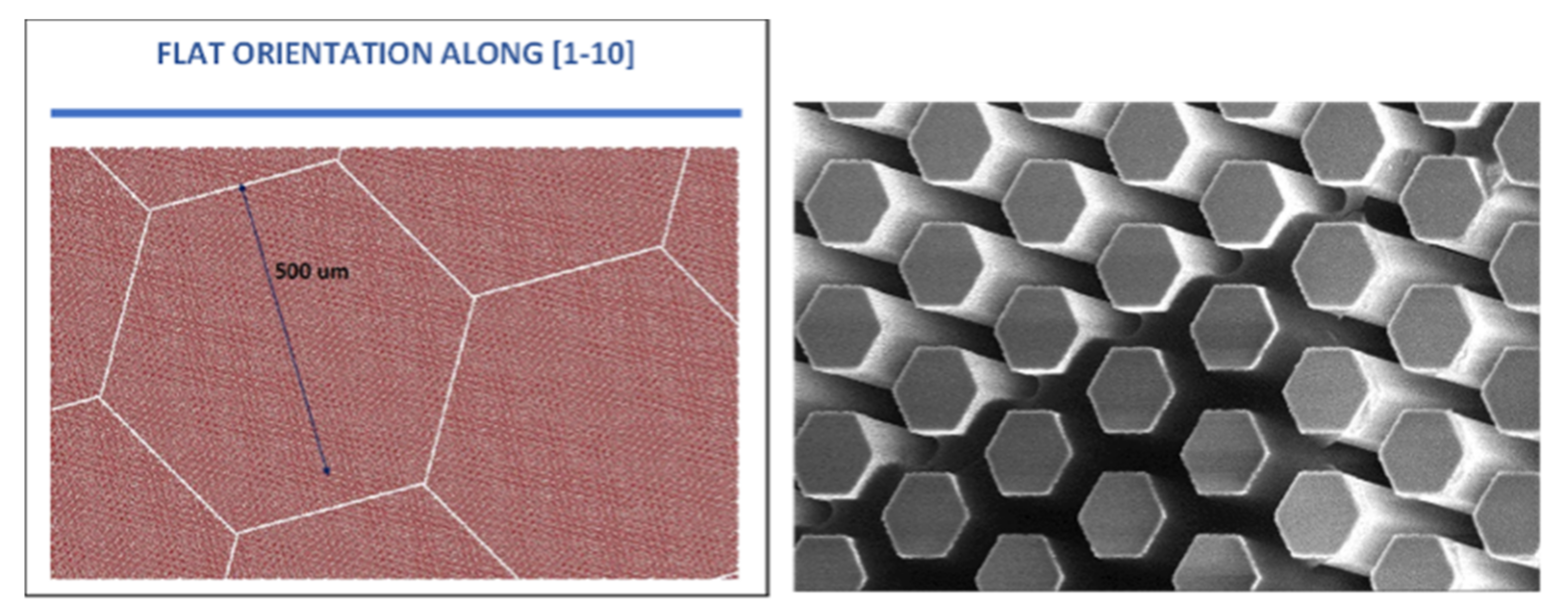
3.2. Compliance Substrates: Pillar Growth
The pillar technology is intended to doctor the thermal strain of the deposited SiC film by growing a suspended (thick) layer on top micrometric Si pillars, which eventually bend to accommodate the larger thermal retraction in the cooling down of the SiC film with respect to the Si substrate. The pillars are patterned in arrays in the Si substrate by a dry etching process [
42,
43] (
Figure 3). The <111> orientation is the most critical one for stress accumulation with film thickness on flat substrates (less than 1 µm without cracks) and also provides a better quality of the deposited material on pillars. Therefore, the shape of the pillars (hexagonal in cross-section) and the arrangement of the arrays (still hexagonal in the pattern), which are suitably rotated with respect to the wafer flat to reduce the slanted 111 facet extension, have been optimized for the <111> growth orientation, wherein the pillar technology could provide the most important contribution.
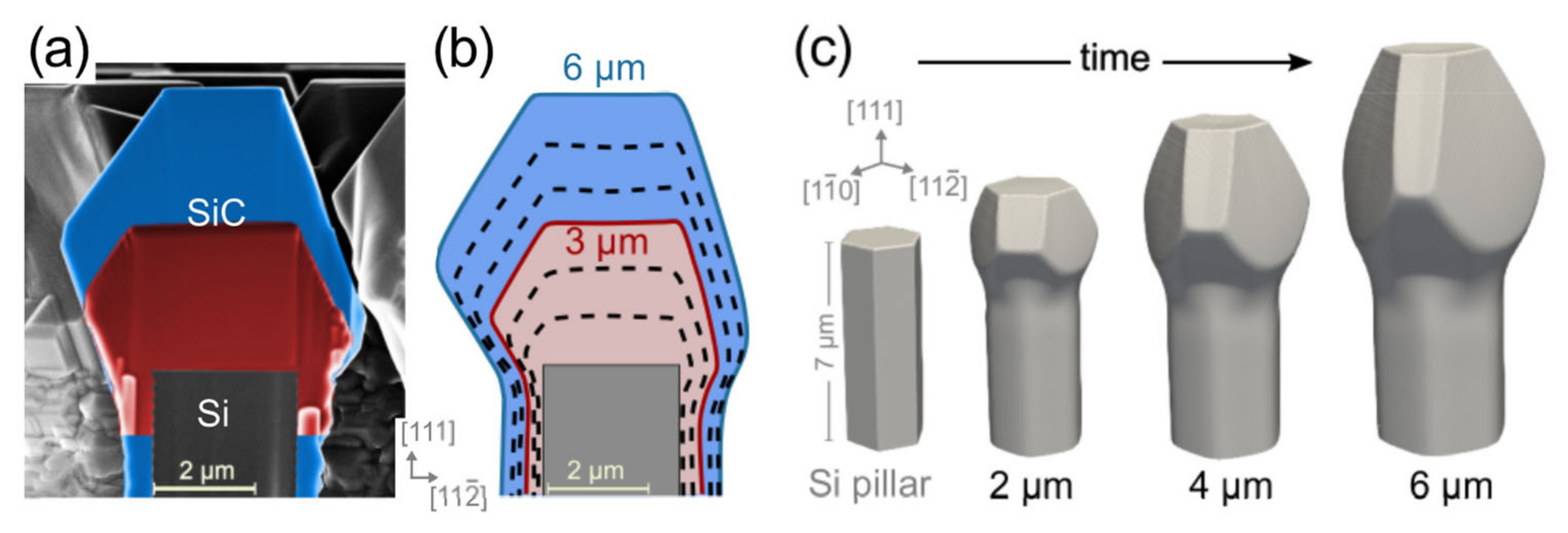
Understanding and controlling the 3D crystal growth and subsequent coalesce dynamics are the keys to optimizing the patterning and obtaining high-quality 3C-SiC suspended layers on the underlying Si pillars. To this goal, an extensive theory-experiment analysis of the evolution of the crystal growth has been performed and detailed in Reference [
44]. First, the faceted growth of the individual SiC crystals has been characterized, as illustrated in
Figure 4, by comparing the profiles of samples grown at different times with phase-field simulations based on the kinetic growth model of Reference [
15]. The unknown facet-dependent growth rates to be set in the model have been extrapolated by fitting the simulation profiles to the experimental ones, resulting in a good match between
Figure 4a and b. Once calibrated, the simulations allow us to investigate all intermediate stages of the growth (c), as well as the subsequent dynamics of merging between neighboring crystals.
As illustrated in
Figure 5, two limiting cases have been studied, corresponding to a 90° rotation of the hexagonal pillar pattern. In case (a), pillar rows are along the [11-2] directions so that coalescence occurs with a six-fold symmetry by bridging the large {111}-C terminated facets with the smaller {100} ones, leaving six identical holes to fill at the latest stages. In the same way, in case (b), pillar rows are aligned along the [1-10] direction such that coalescence occurs at facet edges, resulting in a three-fold symmetry arrangement with a larger hole in between {111}-C facets and smaller ones at the crossing of {100} facets. As made evident by simulations, this latter arrangement is the most convenient, returning a smoother surface profile after the deposition of about 12 µm.
The strain relaxation in the 3C-SiC epilayer is enabled by the tilting of the pillars underneath. As reported in Reference [
45] for the case of Ge grown on Si pillars, the deformation can be described as a rigid-body rotation of each pillar. It is possible to conclude that the capability to rotate strongly depends on the aspect ratio of prismatic (or paralepidid) pillars. Indeed, as shown in
Figure 6a for the pillar at the periphery of the array exhibiting the maximum deformation, the rotation mechanisms and consequently the stress relaxation are larger for a smaller pillar width. Another important parameter that controls the relaxation in the 3C-SiC epilayer is the height of the pillars. Indeed, as observed in
Figure 6b for different patch sizes, the higher the pillar, the better is the strain relaxation. The stress (and strain) relaxation at the center of the array decreases when the patch size is increased, at a fixed pillar aspect ratio, asymptotically matching the reference case without any pillar when the patch size tends to be infinite. The relaxation of the elastic energy in the epilayer can be enhanced also by changing the pillar spacing or, more importantly, the pillar shape. Indeed, if compared to the standard parallelepiped pillars, T-shaped ones (
Figure 6c) offer a higher capability to rotate, being thinner in the intermediate section of the pillar. This results in a lower residual stress or equivalent strain, as shown in
Figure 6a. The T-shape (
Figure 6c) case is comparable to the one with parallelepiped pillars, characterized by a base of half-size and a larger pillar spacing, with the advantage that the T-shape ones have a larger top surface for each pillar, above which the SiC can be grown. According to the approach discussed in Reference [
46], in
Figure 6b, the relation between the width and height of the pillars is plotted to guarantee a curvature radius of the sample that is larger than 10 m. The curvature radius is calculated from the average residual strain in the epilayer according to the Timoshenko formula for planar bilayers [
47].
3.3. Compliance Substrates: SiGe Buffer Layer
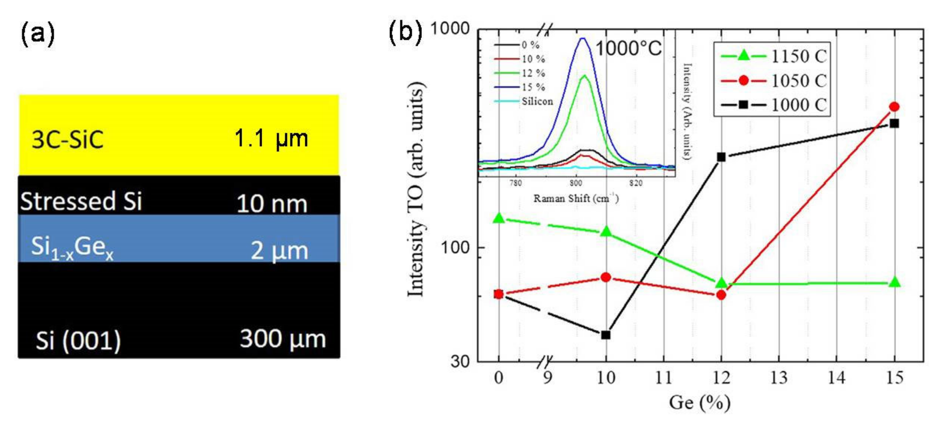
Another attempt to grow a high-quality 3C-SiC epilayer on a silicon substrate was done by introducing a buffer epitaxial layer of Si1−xGex between Si and the SiC. We choose a layer of Si-Ge because Si and Ge have the same FCC structure and are perfectly miscible: the stoichiometry and lattice parameter can be decided a priori. This fact has important implications: fine-tuning the lattice parameter in such a way to minimize the mismatch due to the 4/5 ratio among the Si and SiC atomic layers is possible. Indeed, as already reported, 3C-SiC and Si show roughly a 20% lattice mismatch, implying that four layers of Si almost “equate” to five layers of SiC (the 4/5 rule). The extra plane of SiC creates Lomer and misfit dislocations, thus stacking faults. Nevertheless, the 4/5 rule is not exact and a mismatch (dependent on temperature) also exists between four layers of Si and five of SiC. This mismatch creates stress with the formation of extra dislocations and stacking faults. The adoption of a buffer layer of Si-Ge can also reduce the thermal stress due to the thermal expansion coefficient mismatch (between Si and SiC) caused by the cooling of the sample from the growth temperature (about 1400 °C) to room temperature.
In
Figure 7, we show the structure of the sample used in the experiment: 10 nm Si cap on 2 μm Si
1−xGe
x grown over a 300 μm silicon (0 0 1) substrate. The thin Si capping layer thickness is lower than the “critical thickness” to avoid the formation of interfacial defects at the Si/Si
1−xGe
x interface and it was introduced as a seed for the carbonization step. The intensity of the transverse optical (TO) peak of SiC at 796 cm
−1 is shown in
Figure 7b for different carbonization temperatures and buffer layer compositions. The TO Raman peak is forbidden for perfect 3C-SiC grown on (0 0 1) substrates (due to the selection rules) and its presence is associated with twins and poly-crystals. It was observed that greater Ge content and lower temperatures (1000 °C, 15%; 1050 °C, 15%; and 1000 °C, 12%) lead to a high TO mode intensity. In these samples, we find Ge segregation at the interface between the SiC and SiGe layer. Ge segregation implies the formation of poly-crystals, while samples with lower concentrations and higher carbonization temperatures lead to a mirror-like surface morphology and a lower value of TO intensity indicates a higher SiC quality.
We also demonstrated that the carbonization temperature and composition of the layer control the quality of the SiC film. It is also possible to achieve a higher quality with respect to film grown on virgin silicon [
16].
3.4. Compliance Substrates: Inverted Silicon Pyramids (ISP)
One of the most interesting attempts to grow a high-quality 3C-SiC epilayer on a silicon substrate was done by creating a structured substrate. The structure came from the following consideration: the SFs lie on {111} planes and can interact with each other, stopping the propagation. Consider two SFs laying, for example, in the (111) and (11-1) planes; they can cross and the structure is able to stop the propagation of one or even both SFs. This clearly improves the crystalline quality of the film surface because the SFs remain buried in the epilayer. The rate of SF annihilation is inversely related to SF density, however, by means of the inverted silicon pyramid (ISP) compliant substrate, allowing for a significant drop in SF concentration just within a few microns.
Its unique shape can concentrate SFs in tiny areas, enhancing the phenomenon of SF annihilation [
48].
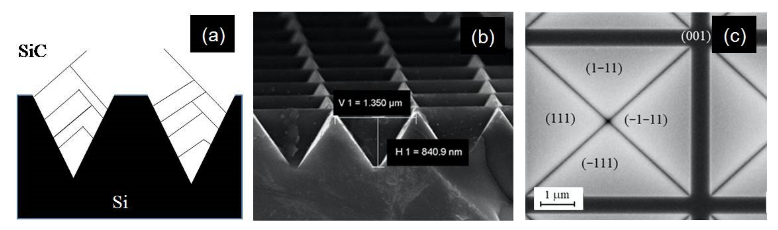
In
Figure 8a, we show a schematic cross-section view of the effect of this compliant substrate. Silicon and silicon carbide are drawn as black and white regions. Blue lines are SFs which either generate an X-shaped defect known as the forest dislocation or self-annihilate, resulting in a system known as the Lomer lock, or end on an existing SF, producing a so-called ”λ-shaped” defect. In
Figure 8b,c, SEM images of the ISP structure are shown in plane cross-view and plane-view. The four (111) planes of the pyramid are shown, as well as the (001) zone among the two pyramids.
The drawback of the use of this substrate is the formation of APB due to the different polarities of the (111) faces of the SiC [
17]. Nevertheless, it is well known that the grain boundary density can be greatly decreased through the enhancement of the film thickness.
The APBs coverage with respect to layer thickness is depicted in
Figure 9a. Despite the fact that the substrate design yields APBs, their concentration was rapidly reduced. Some tenth of microns of the SiC layer is enough to largely reduce the density of APBs. The ISP morphology also induces the formation of buried voids in the epilayer because the (111) face has a slower growth rate than the (100) face. These voids are observed in
Figure 9b in which a cross-view TEM image of the 12 μm-thick epitaxial 3C-SiC layer is shown. The generation of voids may be advantageous in reducing the defectiveness of the epilayer. Voids can annihilate SFs and reduce the residual stress in the layer. SFs that cross the void are not able to propagate into the epilayer, reducing the defectivity. It is also feasible to manage the void height by adjusting the growth rate and conditions. In such a way, it is possible to modulate the concentration of SFs arriving on the surface [
17].
3.6. Hetero-Epitaxy Process: Carbonization
The heteroepitaxy of 3C-SiC on Si is a complex process that is realized in several steps. After the introduction in the reaction chamber, the first step is the etching of the silicon substrate in a hydrogen flux to remove the native oxide (step 1). Then, the second step is the substrate carbonization wherein a flux of the carbon precursor and carrier gas (hydrogen) is introduced in the chamber at temperatures between 900 and 1200 °C (step 2). Subsequently, the temperature should be increased to grow the 3C-SiC layer at temperatures close to the melting point of silicon (step 3). Finally, the temperature is decreased to room temperature (step 4). All these steps have a considerable impact on the quality of the epitaxial layer.
The most critical in the 3C-SiC/Si growth seems to be the second step: the carbonization of the Si substrate. This process is sometimes referred to as “reactive CVD” (R-CVD) because one of the components of the compound (in this case, silicon) is not supplied from the vapor phase but comes directly from the Si substrate that reacts with the gas (“vapor”) species. As a result of carbonization, a thin seed of a few nanometers is formed for the subsequent CVD epitaxy process; it is sometimes denoted as the “carbonization buffer”. The characteristics of this seeding layer are fundamental for the crystalline quality and the stress of the film. From previous studies, it has been observed that for given growth conditions, the morphology and thickness of the carbonization buffer depend strongly on the substrate orientation [
50]. Consequently, the conditions to obtain an optimal buffer differ between orientations. For any orientation, the maximal thickness is conditioned by the nucleation density (proportional to carbon supply) and the ratio between the vertical and lateral growth rates (controlled by process pressure and temperature).
During carbonization, initial nucleation centers extend progressively, laterally, and vertically into three-dimensional 3C-SiC islands. Their temperature-dependent growth rate is proportional to the carbon flow rate but remains limited by the Si supply from the substrate; high in the initial stage when surface coverage with 3C-SiC is low, it reduces progressively to zero as the 3C-SiC islands extend, coalesce, and block the Si supply. It is important to mention that the R-CVD growth mechanism remains active until a complete coalescence of the 3C-SiC buffer is achieved, which is sometimes a long process. Consequently, in many cases, the CVD mechanism coexists (intentionally or not) with R-CVD during the initial part of step 3 of the heteroepitaxial growth.
The roughness of the carbonization layer has a large effect on the stress of the entire film: high roughness makes the relaxation of intrinsic stress during the growth easier [
51]. The main process parameters that influence the roughness of the carbonization buffer are the temperature of the carbon precursor introduction and temperature of the carbonization plateau.
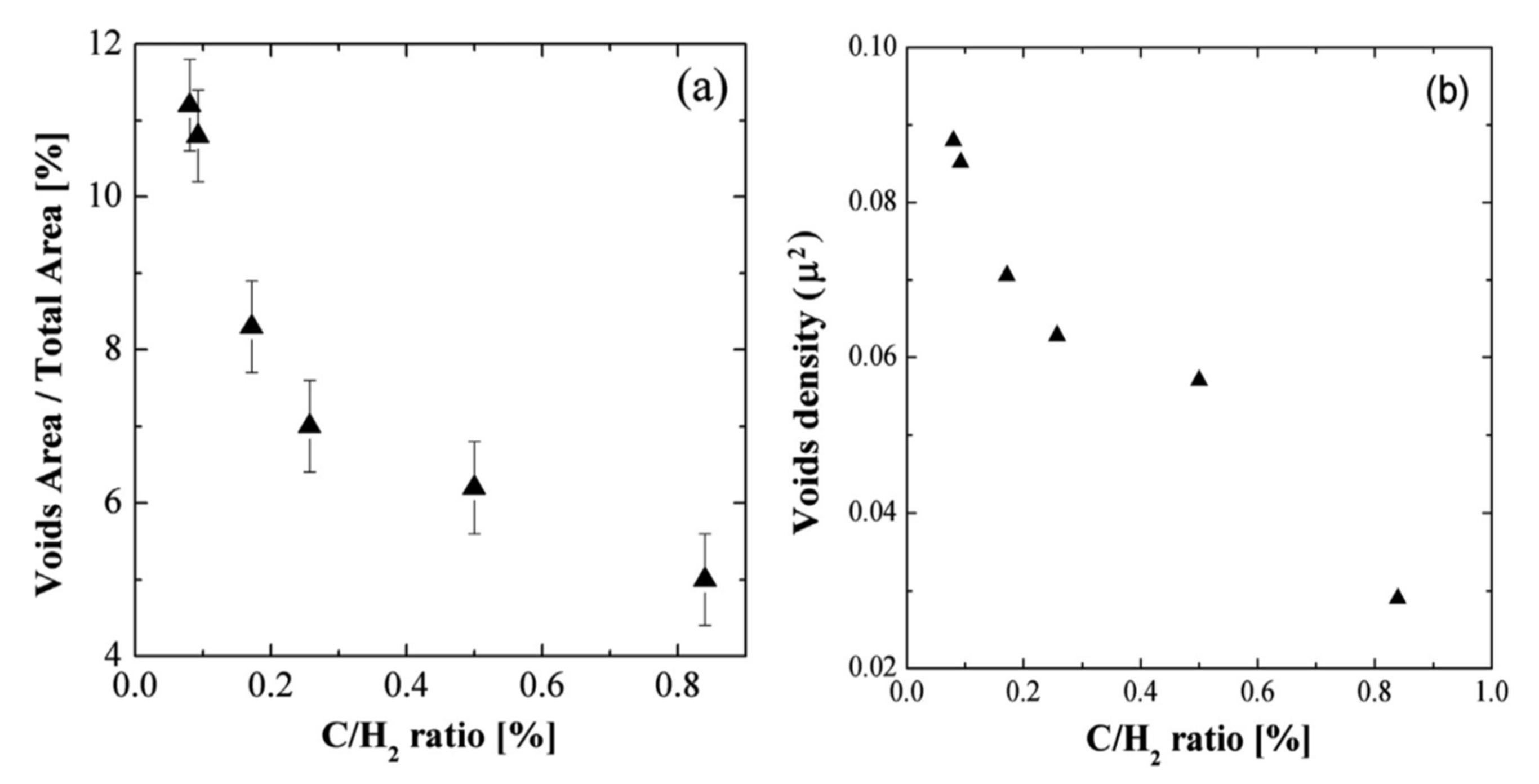
One of the problems related to the carbonization step is the formation of voids (also called “etch pits”) in the near-interface region of the silicon substrate. These micrometric cavities form from the coalescence of silicon vacancies created in the Si substrate as a consequence of the R-CVD growth mechanism. The major part of voids does not affect the quality of the 3C-SiC film (their presence is sometimes considered as a stress-relaxing factor), although some of them can be at the origin of surface defects in the epitaxial film. Consequently, the void formation should be reduced. This can be achieved through carbonization under a high C/H
2 ratio, which increases the nucleation density and favors fast-film coalescence that stops the formation of voids. In
Figure 10a, the fraction in percentage of the void area with respect to the total observed area as a function of the C/H
2 ratio are reported. In the same figure, the density of the void as a function of the C/H
2 ratio is also reported. The effective void areas decreases from 11% to 5% while increasing the flux of carbon atoms. The reduction can be further enhanced by introducing the silicon precursor during the thermal ramp between the carbonization plateau (step 2) and epitaxy (step 3) to form a transition layer. Such intentional mixing of R-CVD and CVD mechanisms further improves the quality of the interface between the 3C-SiC film and Si substrate [
27]. In the same paper, it has been reported that the increase of the C/H
2 ratio also produces an increase in the density of the layer, as well as an increase in the carbonized thickness.
The growth on compliance substrates may require a modification of the carbonization step in order to fit particular substrate-related requirements. This is, for instance, the case for substrates with the Si-Ge buffer for which the carbonization temperature was reduced to below 1000 °C and H2 etching (step 1) was excluded from the process in order to preserve a thin Si cap (10 nm or 20 nm), necessary for correct carbonization. In addition, the temperature of the CVD growth (step 3) was lowered to avoid Si-Ge melting. It is important to underline that such a “low temperature” process resulted in a higher quality of the epilayer on Si-Ge with respect to the film grown on bare silicon.
An alternative approach to the formation of the 3C-SiC seed on the Si substrate was recently proposed. Silicon substrates are “pre-carbonized”, meaning that a few nm-thick amorphous carbon (a-C) film is deposited using the plasma immersion ion implantation (PIII) technique. During H
2 annealing (step 1), carbon reacts with silicon to form oriented 3C-SiC seeds through a solid-state epitaxy mechanism. The standard R-CVD carbonization step is no longer necessary. CVD deposition on such seeds gave satisfactory results on all studied orientations: (100), (110), (111), and (112) [
52].
3.7. Effect of Growth Rate: Defects and Stress
The growth rate has a large effect on the quality of the 3C-SiC both in terms of its structural quality and stress. It has been observed in a previous paper [
53] that the growth rate has a large effect on the density of twins. In fact, in decreasing the growth rate from 10 μm/h to 1 μm/h, a decrease of the twin density of almost a factor of 6 can be observed. A similar (but weaker) effect has been observed also on the rocking curve, which is more sensitive to SFs and point defects [
6]. The Full Width at Half Maximum (FWHM) of the rocking curve is reduced both by reducing the growth rate and increasing the thickness.
With decreasing growth temperature, the growth rate has to be reduced or otherwise the deposition may become polycrystalline. This is particularly the case for 3C-SiC growth on the Si-Ge buffer and constitutes a potential limitation for further development of this approach.
For the 3C-SiC growth on ISP substrates, we demonstrated that the height of the void created above the vertex of the pyramid (
Figure 9b) increased at higher growth rates. Consequently, the initial stage of 3C-SiC growth on ISP substrates, until reaching complete coalescence, should be performed at a low growth rate.
The growth rate has also an influence on the final stress of the 3C-SiC epilayer. Indeed, as demonstrated in [
54], during the growth of the 3C-SiC layer, the intrinsic stress in the layer is continuously relaxing. For a given film thickness, by tuning the growth rate, we can adjust the duration of the relaxation (by the duration of the growth), controlling the final stress of the sample.
3.8. Defects in 3C-SiC: SFs and APBs
In 3C-SiC, the most important defects that hinder its use in the microelectronic industry are related to SFs and dislocations. Stacking faults (SFs) are the most important ones dominating over the entire 3C-SiC layer thickness. In literature, three types of SFs are observed depending on the number of atomic planes with the wrong orientation: SFs can have 1, 2, or 3 errors in the stacking sequence and they are called intrinsic (or SF<1>), extrinsic (or SF<2>), or conservative (or SF<3>) [
40,
55,
56].
In 3C-SiC, mechanisms for SFs’ self-annihilation exist but there is also the possibility for SFs to be generated [
6,
40,
57,
58]. The concomitant presence of these mechanisms leads to the fact that SFs in 3C-SiC can be hardly reduced. The minimum SFs’ densities achieved so far amount to about 10
4 cm
−1 in thin films [
58]. In
Figure 11a, a TEM image in in-plane view shows four stacking faults that are generated from a grain boundary, while in
Figure 11b, a TEM image in cross-view shows the annihilation of the SF. In
Figure 11a, a vertical grain boundary generates three clearly visible SFs lying in (
), (
), and (
) planes. Interestingly, two SFs in the (
) planes limit the SF in the (
) plane; they are limited on the other side by the grain boundary. The intersection between the SFs (
) and (
) is the Lomer−Cotrell partial dislocation and has a Burgers vector of a/6[011 The place in which the grain boundary intersects the SF (
) is the place in which the SF (
) is generated. In
Figure 11b, the crossing of several SFs is shown. This image proves that there are two possible intersections of the SF lying in the (111) and (
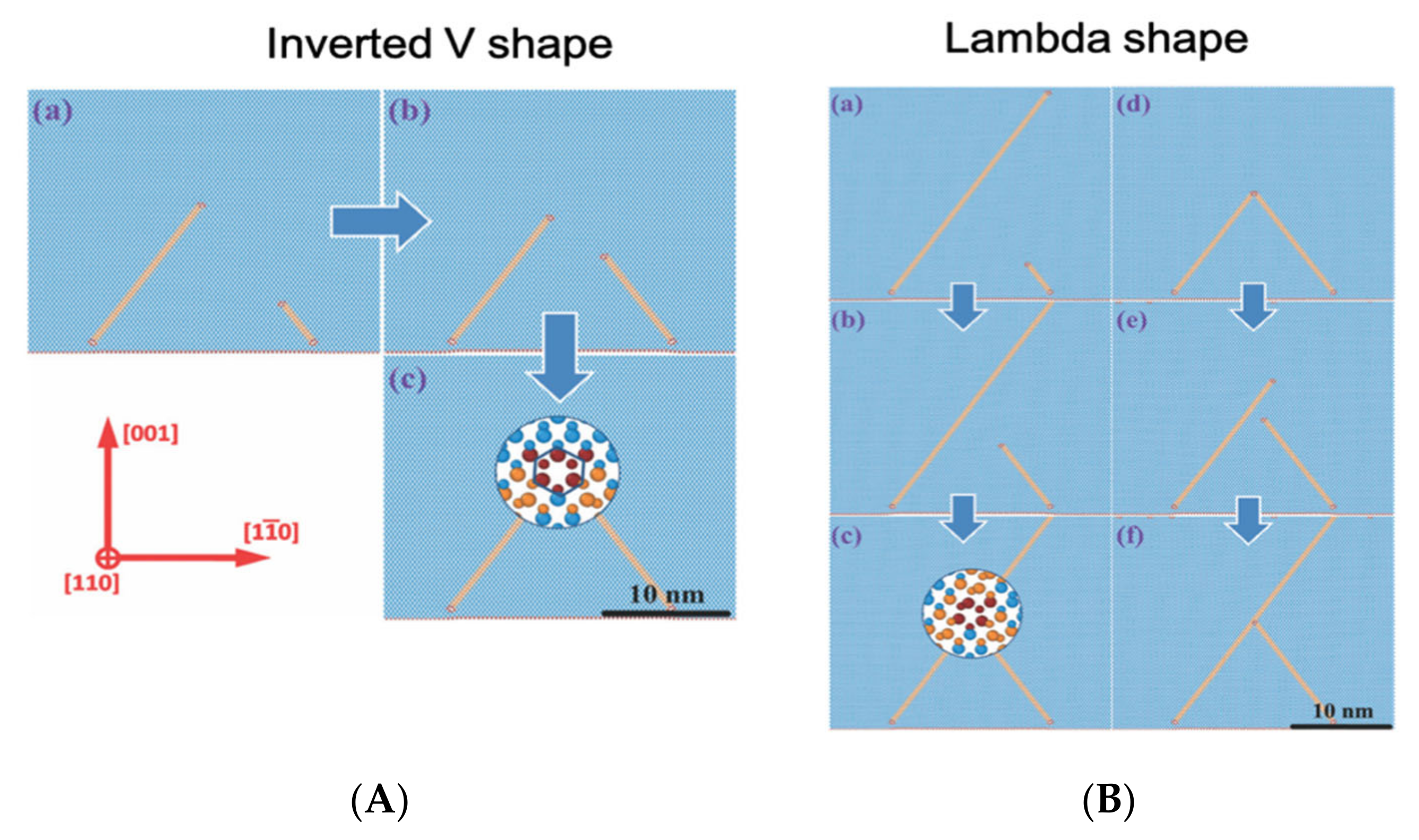
) planes. The intersection indicated as “1” has an inverted V-shape typical for the formation of a Lomer–Cottrel dislocation. This dislocation, as already reported, has a Burgers vector (a/6[110]) lower than the usual partial dislocation Burger vector (a/6[112]) that borders the stacking fault. The intersection called “2” has a lambda shape; it forms for kinetical reasons. These two configurations can decrease the amount of SF approaching the surface and improve the quality of the epitaxial film.
The annihilation mechanism is considered in more detail in Reference [
59]. It is found that the key parameter for the formation of a lambda-shape or an inverted V-shape is the distance between the PDs and the mutual orientation of their Burgers vectors. In the case in which the PDs have Burgers vectors that sum in such a way that the resulting Burger vector is shorter than the initial ones, the partial dislocation attracts to each other and if they are closer by less than about 15 nm, the propagation of both SFs is suppressed with the formation of a Lomer–Cottrell lock. In the case in which the two PDs are far more than 15 nm, they do not interact with each other and can form a Lambda-shape structure. The Lambda-shape can form even if the partial dislocations are close enough, but they repulse. In
Figure 12 on the left, a sequence of MD simulation snapshots of the formation of “inverted V”-shaped intersection of stacking faults have been shown. In
Figure 12 on the right, MD simulation snapshots of the formation of “λ”-shaped intersections of stacking faults in the case of a large distance between partial dislocations (a–c) and repulsing dislocations (d–f) have been reported. Blue atoms correspond to the Si and C atoms in the cubic diamond lattice, while orange atoms belong to the stacking faults.
The SFs can interact also with other extended defects, such as the inverted domain boundary (IDB) (sometimes called the anti-phase boundary, APB). In 3C-SiC grown on (100) “on-axis” silicon, due to the symmetries of the Si lattice, two equivalent dispositions of the SiC crystal are possible. The two possible orientations are rotated 90° around [001] and, due to the SiC symmetries, a rotation of 90° is equivalent to flip the crystal upside-down. The boundary between two such domains is called IDB (or APB). The SFs can interact strongly with this kind of extended defect of SiC. In
Figure 13, a sequence of STEM images showing an IDB interacting with SFs is shown. The image is the projection of the TEM lamellae in the (110) plane. The SFs are observed as straight lines, while the IDB has different lying planes and appears as a ribbon. A close inspection of these images shows that SFs can be generated and annihilated by the IDB: several SFs can be recognized in the figure and some of these are apparent only in the crystal below the boundary, while some others are apparent only in the crystal above the boundary. SFs that are in the lower crystal are not allowed to propagate in the top crystal and in this case, we observe an annihilation of the SF due to the presence of IDB. On the contrary, SFs that belong to the top crystal and are not present in the lower crystal are generated in the IDB. The SFs can be generated during the growth due to interface instability that creates seeds for nucleation; after the nucleation, it expands following the growth of the surface. Eventually, it can collide on an IDB and be annihilated [
40]. SFs can be also generated during the cooling down of the temperature after the growth; indeed, temperature gradients can induce stress in the layer. Above critical shear stress, it is known that the formation of dislocations and, in 3C-SiC, the formation of partial dislocation is a thermodynamically favored process.
As previously discussed at the beginning of
Section 3.7, different kinds of SFs are present in 3C-SiC. These different types of SFs can be seen as inclusions of different hexagonal polytypes in the cubic structure. In particular, the intrinsic SF can be called a 2H-like SF, the extrinsic one can be seen as a 4H-like SF, and the conservative one can be seen as a 6H-like SF. These different SFs have different energies [
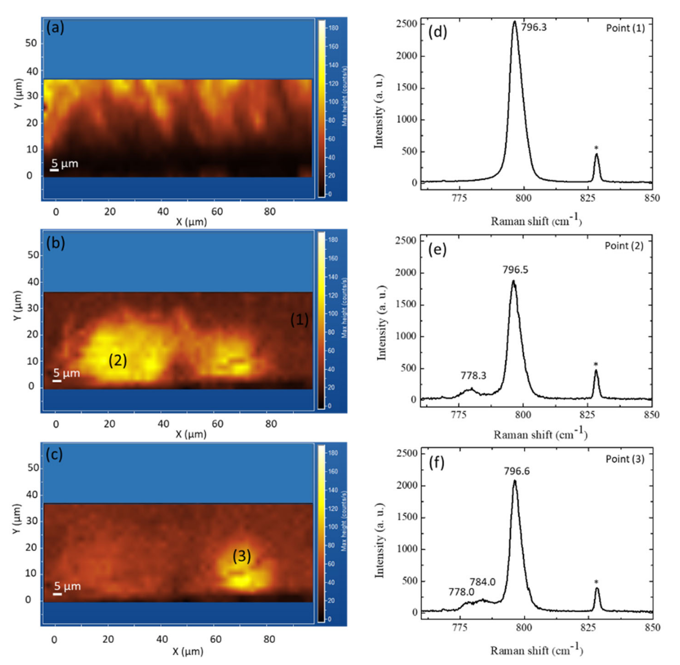
60] and different behaviors of these defects should be expected. The room temperature μ-PL map at 540 nm, taken on a 3C-SiC sample in cross-section, is shown in
Figure 14a [
61]. Moving from the Si-SiC interface towards the top (from 0 μm to 35 μm), the band-edge peak intensity rises, showing a considerable improvement of the crystalline quality, increasing the growth thickness.
Figure 14b,c exhibits μ-Raman maps obtained in the same location and indicate certain areas as well as the 3C-SiC/Si interface with greater signal magnitude at 778 cm
−1 and 784 cm
−1, respectively.
Figure 14d–f displays the mean Raman spectra obtained in areas (1), (2), and (3), which reveal the 3C-SiC TO mode centered at about 796.5
0.2 cm
−1. Conversely, the mean Raman spectrum obtained in points (2) and (3) reveal an extra peak at 778.3 cm
−1, as well as two more peaks correspondingly at 778.0 cm
−1 and 784.0 cm
−1. These additional peaks can be related to the presence of extrinsic (4H-like and 6H-like) stacking faults. From these data, we can observe that, despite the low energy of the 6H-like SF, it appears that this kind of stacking fault can be observed in larger regions and closer to the surface with respect to the 4H-like SF. More investigations should be done concerning this aspect but we suspect that this large presence of 6H-like SFs could be due to kinetic reasons more than energetic ones. In fact, from the energetic point of view, this SF has the lowest formation energy.
3.9. Defects in 3C-SiC: Kinetic Monte Carlo Super Lattice Simulations
The study of the kinetic evolution of a defective system is a difficult task as it requires both atomistic accuracies typical for the molecular dynamics approach and large space-time scales typical for the experimental systems. Within the CHALLENGE project, we developed an ab-initio calibrated kinetic Monte Carlo super lattice (KMCsL) code, [
62] offering a good compromise between accuracy and efficiency, which can simulate the results of the growth processes in non-polar SiC as a function of the growth parameters also in terms of defectivity and surface morphologies. Hence, the KMCsL simulations allowed for the investigation of the formation and development of extended as well as point defects over a realistic growth [
62]. As an example of a simulation application strongly relevant to the experimental studies, we considered the evolution of anti-phase boundaries (APBs) in 3C-SiC and their interaction with stacking faults (SFs), which is discussed in detail in Reference [
57].
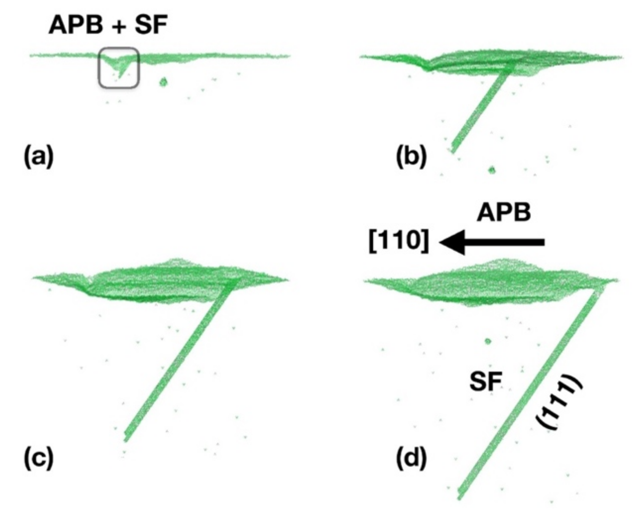
Due to the comparable energetics of polytypes, SFs are a frequent and wide-spread extended defect in SiC, with respect to the polytype. They are classified as incorrect atoms sequences in comparison with theoretical polytype stacking arrangements. In the purely hexagonal close-packed (hcp) representation, the polytype sequence is defined as a repeating series of layers made up of Si-C dimers aligned on the hexagonal axis. Dimers in every layer take one of three extremely symmetric locations (often denoted as A, B, and C). If the recurring arrangement is ABC ABC ABC…, etc., extending along the crystal <111> axes, the cubic 3C-SiC (zinc-blend) configuration is produced. As a result, the existence of {111} planes on the surface depletion allows for an increase in SF production. The formation of a pair of triple SFs (SF <3>: three bilayers not in the correct crystalline structure) from the surface depletion caused by an APB is shown in
Figure 15. A series of pictures of the under-coordinated atoms obtained at various KMC intervals are displayed. The existence of three-fold coordinated Monte Carlo particles at its border leads to the generation of the triple SF in this depiction (i.e., at the corresponding partial dislocation). We note that the stacking sequence of the triple SF (sometimes termed micro-twin, i.e., ABC ABC ACB ABC ABC ABC) divides two crystal areas in pristine epitaxial order. The only atoms out of the right crystal locations are those within the extended defect. The APBs’ localized asymmetry as well as the existence of the {111} faceted surface result in the development of a triple SF (due to polytype instability) (see
Figure 15a,b). When the APB generates the SF, the two extended defects (SF and APB) maintain separate kinetics: the APB proceeds to move through the [110] plane, while the SF expands on the (111) plane (snapshots b, c, and d of
Figure 15). A TEM picture of an SF generated by an APB along the epitaxial growth of a 3C-SiC (001) substrate is shown in
Figure 15e. It expands autonomously from the APB kinetics along the {111} planes. Moreover, surface depletion can be seen in the correspondence of the (001) surface. These composed structures of proximal APB and SF-type defects have been also evidenced by the conductance maps in this paper.
3.10. Defects in 3C-SiC: Electrical Effects
Nanoscale-resolution current mapping of 3C-SiC by conductive atomic force microscopy (CAFM) provided a direct demonstration of APBs as the main extended defects responsible for the enhanced leakage under reverse-bias, whereas both APBs and SFs were shown to act as current paths under forward polarization.
Figure 16a illustrates the experimental configuration used for CAFM measurements on the cubic silicon carbide surface. A typical topographic image collected on a 20 μm × 20 μm scan area is shown in
Figure 16b, from which a surface root mean square (RMS) roughness of 3.2 nm was calculated. The nanometer deep “V-shape” depression in the morphology and in the height line-scan (
Figure 16b, right panel) were associated to an APB in accordance with the Monte Carlo simulations of
Section 3.7.
Figure 16c,d report the current maps measured simultaneously to the topography by applying a reverse-bias (V
tip = −0.5 V) and forward-bias (V
tip = 0.5 V) polarization to the Pt tip, respectively. This Schottky diode behavior of the Pt/3C-SiC contact was confirmed by the significantly lower current values measured under reverse polarization with respect to those measured under forward-bias. Using the same current range (from 0 to 50 pA) for the two current maps, APBs are the most evident conductive features under reverse-bias, whereas both APBs and SFs (indicated by blue arrows in
Figure 16d) contribute to the conduction under forward polarization. Two representative scan lines across the APB for the two opposite tip biases are also shown in the right panels of
Figure 16c,d, showing a higher current peak on the APB under forward-bias with respect to the reverse one. This suggests that APBs are mainly responsible for the enhanced reverse leakage current measured in macroscopic Pt/3C-SiC Schottky diodes. In particular, the separation between these extended defects deduced from this microscopic analysis is in the order of tens of micrometers, in very close agreement with the value of L (≈20 μm) deduced from the statistical characterization of Schottky diodes with different areas for thin 3C-SiC layers [
63].
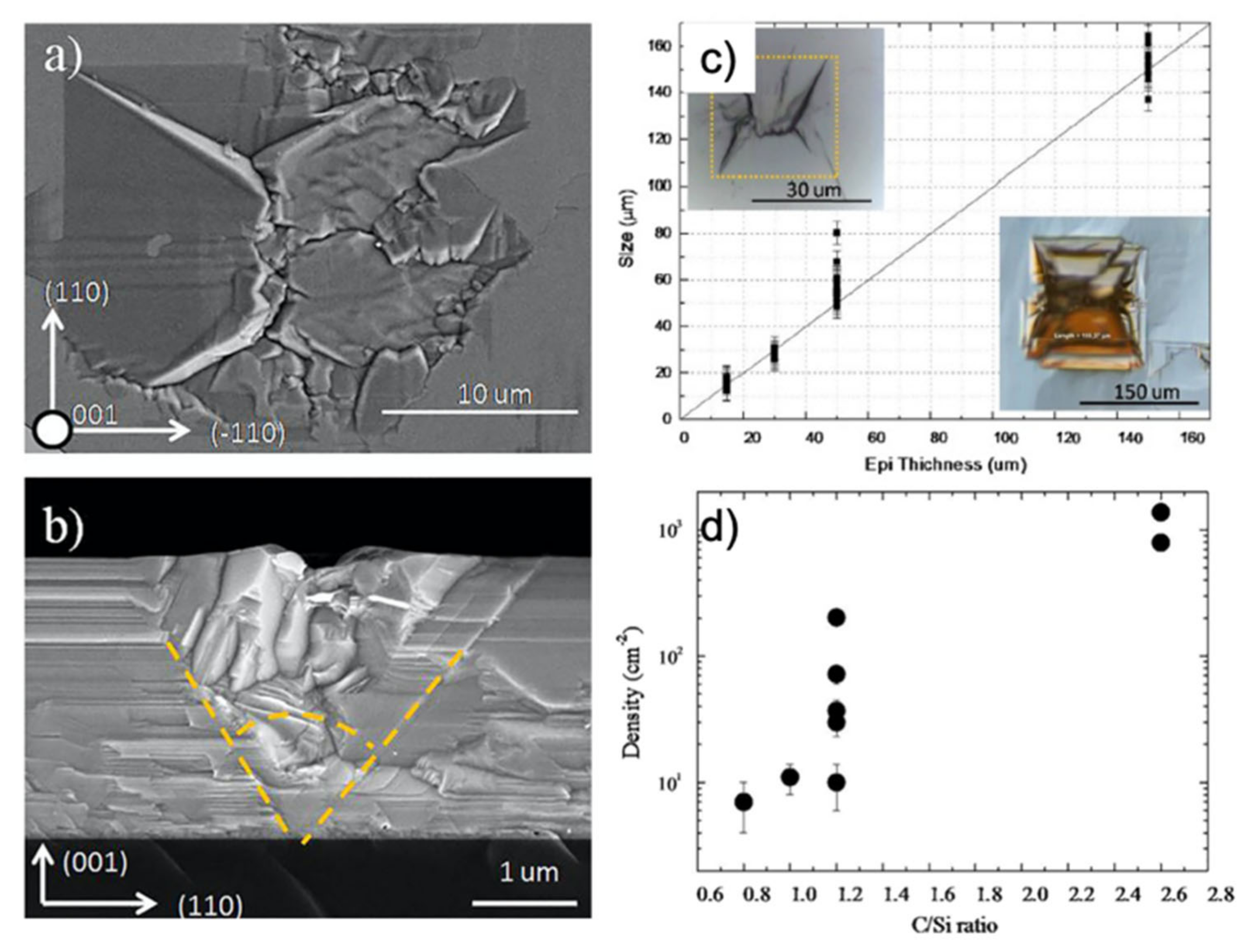
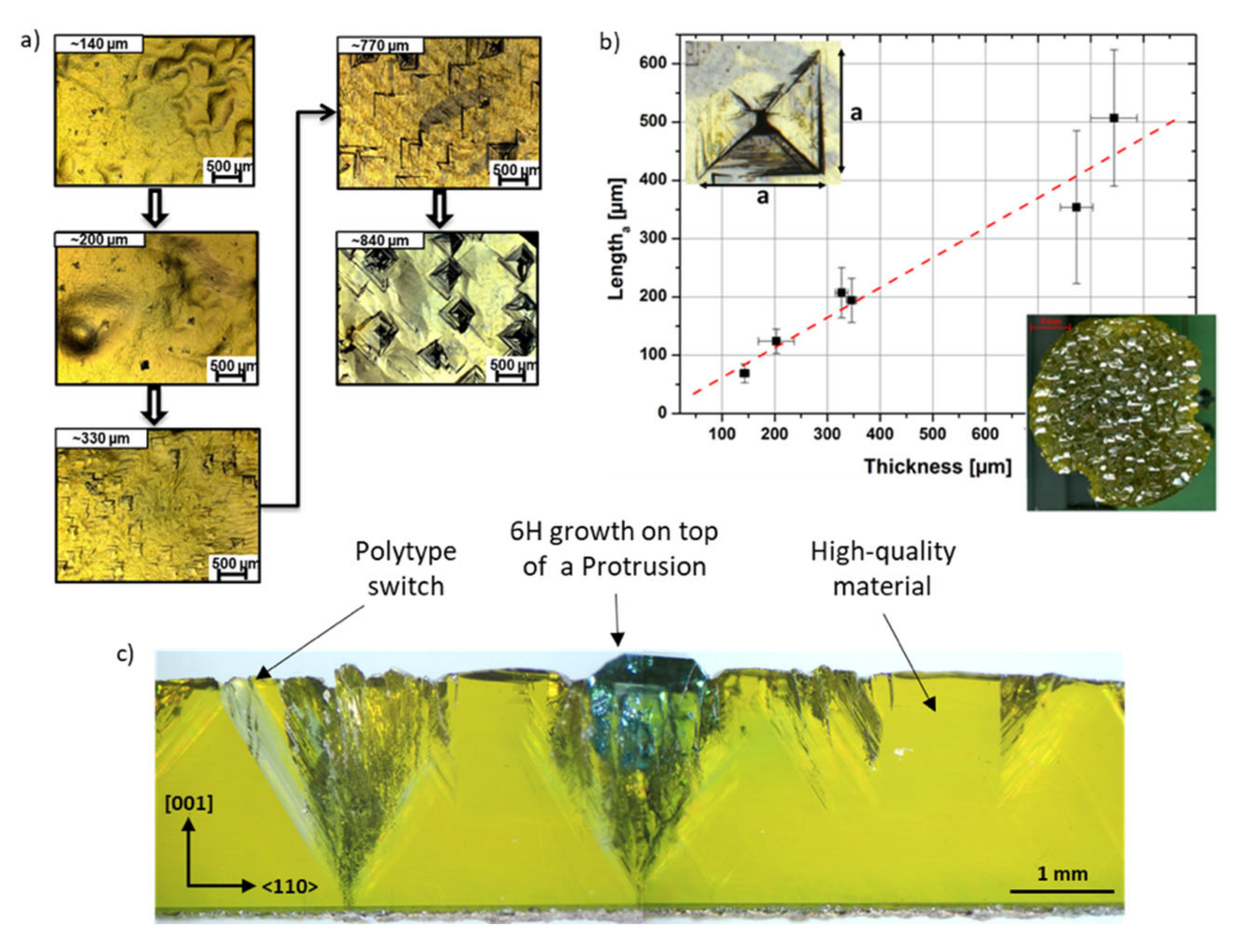
3.12. Defects in 3C-SiC: Protrusions
Small defects produced during the carbonization process can have a large influence on the final wafer quality: an example of this effect can be seen in the case of the defect called “protrusions”. These defects appear on the surface of 3C-SiC as dark squares, with a peculiar 3D structure similar to inverted pyramids with a vertex close to the SiC/Si interface. In
Figure 17a,b, a scanning electron microscope image of protrusion in in-plane (a) and in cross-view (b) are shown. [
67] The plan-view image is shown for a 30 μm-thick epilayer to evidence the shape of the structure, while the cross-view is shown for a 3 μm-thick epilayer. Yellow lines are drawn to identify the edge of the defect that is limited by four stacking faults. It was also found that the inner core of the defect consists of nano-crystals twinned with respect to the substrate orientation. The base of the inverted pyramid is a square and the height is the same as the thickness of the epilayer. In
Figure 17c, the lateral size of the protrusion is shown as a function of the epilayer thickness. A linear correlation between the size of the protrusion and the thickness of the epilayer is apparent. Again in
Figure 17c, two optical images of the protrusion are shown: in the left-upper corner, a defect in the 30 μm-thin film is shown, similar to what was observed in
Figure 17a, while in the right-lower corner, the defect in the 150 μm-thick film is shown. Since the quality of the layer depends strongly on the thickness, a higher thickness is preferable. Thus, the presence of even a small density of protrusions must be indeed avoided because it can strongly decrease the quality of the wafer. In stating the importance of reducing the density of such a defect, our group investigated the reason for the formation of protrusions. The seed of this extended 3D defect lies 10 nm above the SiC/Si interface and is probably related to a non-balanced carbon amount during the carbonization step or during the temperature ramp-up after carbonization. Carbonization, as earlier reported, is a process in which the carbon precursor reacts with the bare silicon surface and this is performed to prepare the Si surface for SiC growth. The Si/C ratio during the carbonization and the post-carbonization process is the key parameter to avoid the formation of protrusions. In
Figure 17d, the density of protrusions as a function of the C/Si ratio during the rise of the temperature after carbonization is shown. As it is apparent, a ratio lower than 1.2 is able to decrease the density of protrusions by almost two orders of magnitude, leading to a density of 10 cm
−2.
3.13. Stress in 3C-SiC
Another aspect that is crucial in the development of the 3C-SiC material is stress. In this case, we have essentially two different components of the stress:. The first one is called intrinsic stress, related to the different lattice constant between 3C-SiC and the silicon that produces a high concentration of defects at the interface. These defects produce a high level of stress essentially in the first microns of the growth. For thick layers, we observe a reduction of this intrinsic stress and for very thick layers, this component of the stress is close to zero. For the intrinsic stress, it has been observed through using MEMS devices that the reduction of the stress follows an exponential low that is very close to the exponential decrease of the SFs’ density vs. thickness [
9]. This stress is generally compressive in 3C-SiC (100) while it is tensile in 3C-SiC (111).
The second component of the stress is the “thermal stress”, related essentially to the different thermal coefficients between silicon carbide and silicon. In fact, the growth occurs at high temperatures (1350–1390 °C) and the two materials (SiC and Si) decrease their lattice constants in different ways, moving from the growth temperature to room temperature. This component of the stress is always tensile and then reduces the stress or even changes the sign of the stress in the (100) material, while considerably increasing the total stress in the case of the (111) 3C-SiC. For this reason, it is extremely difficult to grow a thick layer of 3C-SiC on the (111) Si without cracking the film or even the substrate during the ramping down of the temperature in the reactor.
In the CHALLENGE project, we used two different approaches to try to solve this problem. The first approach has been described in
Section 3.2. In fact, using the pillars’ structures, it is possible to considerably reduce the thermal stress with the deflections of the pillars on the edge of different patches (see
Figure 7). In this way, it was possible to obtain thick (111) 3C-SiC layers’ wafers with a low bow.
The other approach that we used in this project will be described later in
Section 3.15. In this approach, after a thick growth (60–90 μm), the silicon substrate was melted inside the reaction chamber and then removed one of the sources of the thermal stress. Obviously, this process does not remove the intrinsic stress due to the defects at the 3C-SiC/Si interface. Using the SiGe buffer layer approach described in
Section 3.3, it is possible to decrease the intrinsic stress but further experiments should be done to completely remove this component.
3.14. Bulk Growth on Hexagonal SiC
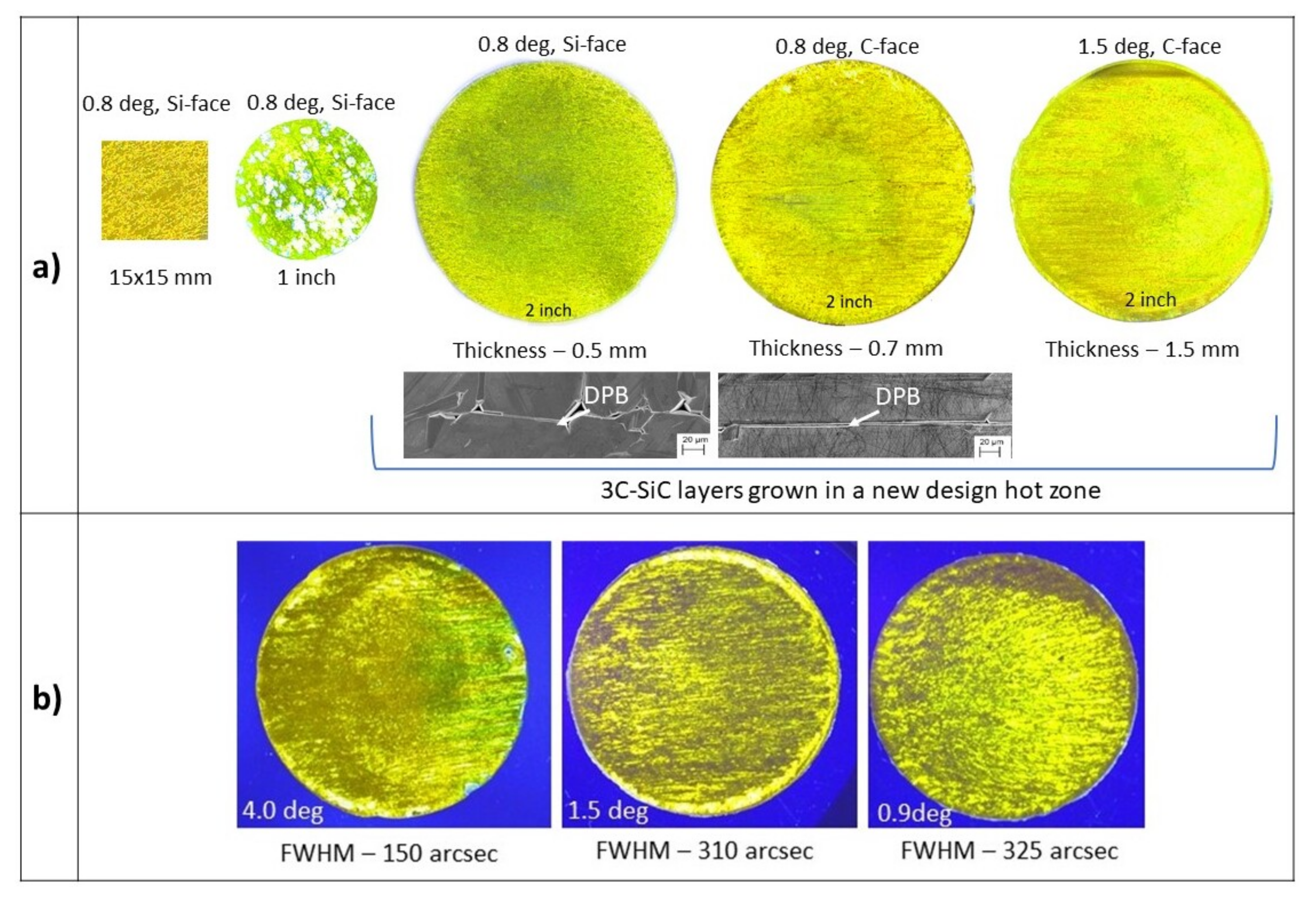
As demonstrated [
21,
22], during the initial stages of the growth, a facet with an on-axis surface is formed at the edge of the grown layer. At specific growth conditions, this facet becomes a preferential 3C-SiC nucleation site. Once 3C-SiC is formed on the facet, it laterally enlarges by covering the entire surface. The lateral enlargement of 3C-SiC from the edge towards the center on the SiC (0001) surface is proportional to ~ tan α, where α is the off-cut angle of the substrate. Therefore, by increasing the off-orientation of the substrate, the total layer thickness needed to cover the entire substrate surface, with the 3C-SiC enlarging from the edge of the sample, also increases. Based on our estimations, to cover a 1-inch 4 degrees off-oriented hexagonal SiC (0001) substrate with 3C-SiC, the layer thickness should be about 4–5 mm. Such a thickness complicates the growth process. Therefore, as a compromise, a hexagonal substrate with a 0.8 degrees off-cut was used to explore the growth on a larger substrate area. As seen on the left side in
Figure 18a, a full surface coverage with the 3C-SiC on hexagonal substrates with the size 15 × 15 mm
2 was obtained. However, when the same growth conditions (T = 1900 °C, average growth rate of ~0.3 mm/h) were applied to the growth on 1-inch substrates, an instability of the 3C-SiC polytype was observed. This was attributed to the dimensional limitations of the graphite container, which does not allow for the obtaining of the uniform supersaturation of SiC vapor species over the entire surface of the substrate. Therefore, a new hot zone for the growth of 3C-SiC on 2-inch substrates was designed and the immediate advantage of it in controlling the stability of 3C-SiC was observed. However, by growing thicker layers on (0001)/Si-face substrates, it was observed that the DPBs tended to branch out into larger structural defects, which deteriorates the quality of the 3C-SiC crystal. To compare the formation of DPBs, the growth of 3C-SiC on the (000-1)/C-face was investigated. It was observed that there was an obvious difference in the DPBs’ appearance in the 3C-SiC grown on the (000-1)/C-face. As shown in the scanning electron microscope (SEM) images in
Figure 18a, the majority of DPBs on the (000-1)/C-face maintain a line-like propagation path. This means that their propagation is less damaging to the 3C-SiC crystal compared to the ones on the Si-face. In addition, an interesting phenomenon indicating different step dynamics in 3C-SiC layers grown on the Si and C-faces has been observed. Surfaces analysis by atomic force microscope demonstrated that the step-height in both cases is very similar and mostly varies between 0.25 and 0.8 nm, while the terrace width is almost three times larger on the Si-face and varies in a range of ~130–150 nm. The crystalline quality of 3C-SiC layers grown on the Si and C-face on substrates with the same off-cut angle of 0.8 degrees is similar and the full-width at the half-maximum of the XRD ω rocking curve using a footprint of 5 × 5 mm
2 varies between 200 and 300 arcsec. However, 3C-SiC layers grown on the C-face of a hexagonal substrate with the off-cut angle of 1.5 degrees contain areas with ω rocking curve values of 93 arcsec. This indicates that using hexagonal SiC substrates with even higher off-cut angles could be the right direction for further research, even though the growth on such substrates will require growing much thicker layers to obtain a full coverage with 3C-SiC. Therefore, a comparative study of the 3C-SiC(111) grown on the (0001)/Si-face and (000-1)/C-face on 4 degrees off-oriented 4H-SiC research size (7 × 7 mm
2) substrates was conducted [
68]. Even though the 3C-SiC polytype is more stable on the (0001)/Si-face, it was shown that smoother surfaces of 3C-SiC could be obtained on the C-face. In addition, the transition layer, which is a mixture of various polytypes, between the hexagonal SiC substrate and the 3C-SiC is significantly thinner on the (000-1)/C-face, leading to a direct polytype conversion mechanism.
Based on the promising results on the growth of 3C-SiC on the (000-1)/C-face of 4 degrees off-oriented 4H-SiC research size (7 × 7 mm
2) substrates, a series of experiments were done on a 2-inch area. An example of a 2.5 mm-thick 3C-SiC layer grown on a 4 degrees off-oriented substrate is shown in
Figure 18b (picture on the left). The 3C-SiC layer grown on 4 degrees off-oriented substrates still contains double-positioning boundaries that deteriorate the crystalline quality. Despite that, when compared to 2.5 mm-thick 3C-SiC layers grown on substrates with lower off-orientations, the crystalline quality is higher. This was confirmed by the FWHM of HRXRD ω rocking curves, which were measured on three different areas on each layer using a footprint of 2 × 10 mm
2. The average FWHM values of 3C-SiC layers grown on 4.0, 1.5, and 0.9 degrees off-oriented SiC substrates were 150, 310, and 325 arcseconds, respectively. This indicates that even larger off-orientations could be a potential route for the further improvement of 3C-SiC crystalline quality.
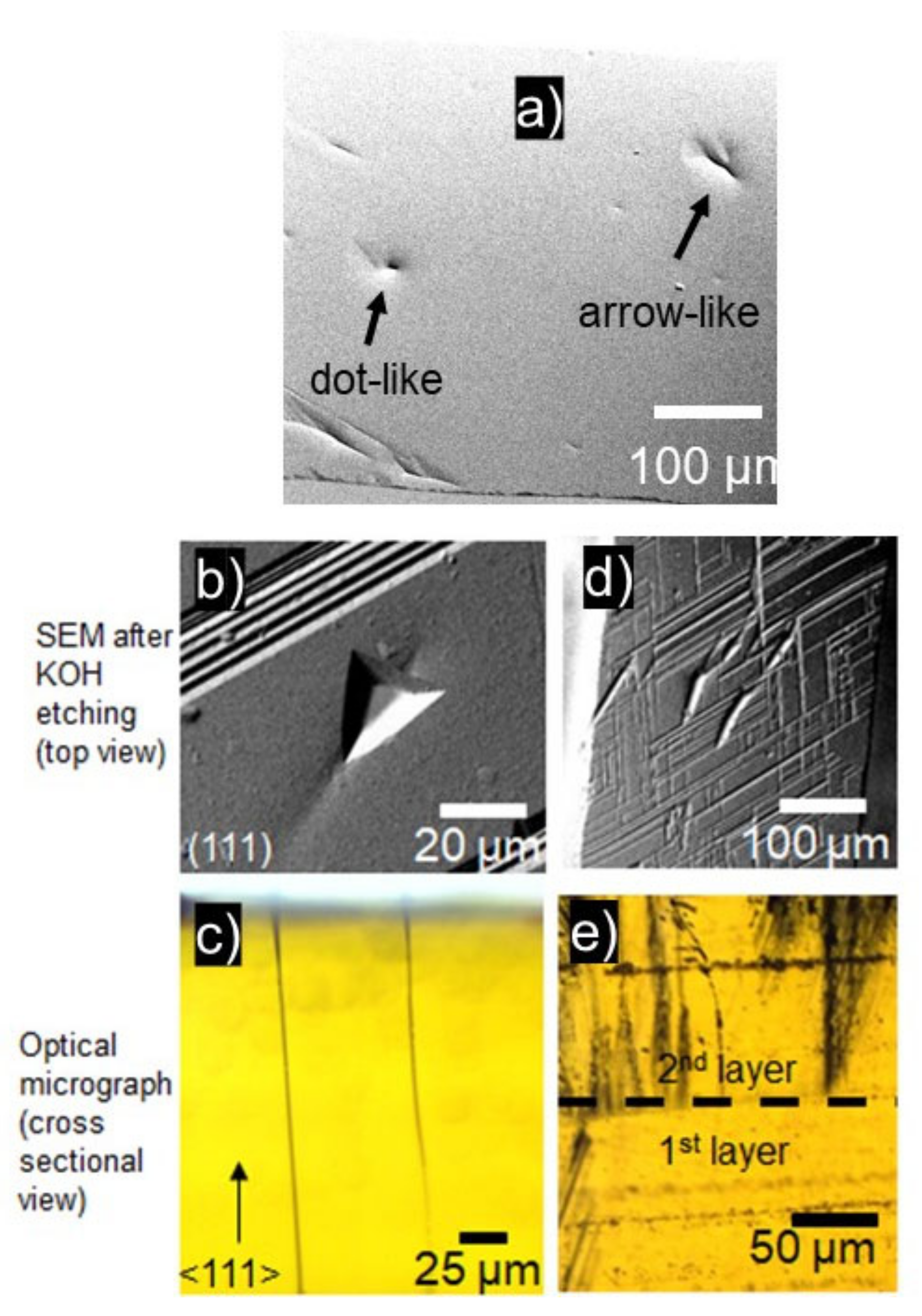
In addition to DPBs, which are dominant defects in 3C-SiC grown on hexagonal SiC substrates, dot-like and arrow-like defects are observed (
Figure 19a). These defects usually occur in samples that are thick (>1 mm) and grown by interrupted growth (growth stopped to change polycrystalline SiC plate/source). After selective etching using molten KOH, the dot-like defects appear as triangular etch pits (
Figure 19b), which are characteristic features of threading screw dislocations on the (111) crystal surfaces. The selective etching of arrow-like defects revealed elongated groves as shown in the SEM micrograph in
Figure 19d. In addition, after KOH etching, the surface around the elongated grooves possessed imprints of stacking faults propagating along (111) planes, which appeared as line-like features rotated to each other by 60 degrees. Based on cross-sectional analysis by optical microscope, the dot-like features on the surface corresponded to the threading defects with a cylindrical path that did not widen while the crystal grew (
Figure 19c). They originate in the grown 3C-SiC layer, transition layer, or can be tracked down all the way to the substrate. In the latter case, they can be observed as a continuation of micro-pipes propagating in the substrate material. The arrow-like defects can originate anywhere in the 3C-SiC layer but the most common origin is at the interface between 3C-SiC layers grown by repeated growth runs as shown in
Figure 19e. This indicates that thick (>1 mm) 3C-SiC layers should be grown in a single growth run. Otherwise, disturbances in the growth during the cooling down and temperature ramp-up processes may cause the formation of such defects. Moreover, as the thickness of the 3C-SiC layer increases, the arrow-like defects tend to branch out and significantly deteriorate the crystal quality. The formation of such defects can be tackled by using thicker source-material, which would allow for growing thick layers without any interruption.
Even though the defect density in the 3C-SiC grown on hexagonal SiC over the 2-inch area is too high for the industrial processing of transistors, it could be used to explore hydrogen generation using solar-driven water splitting [
69] or the growth of a large-area monolayer and multilayer graphene [
70,
71].
3.15. Close-Space PVT Growth of Bulk 3C-SiC on 3C-SiC-on-Si CVD Seeding Layers
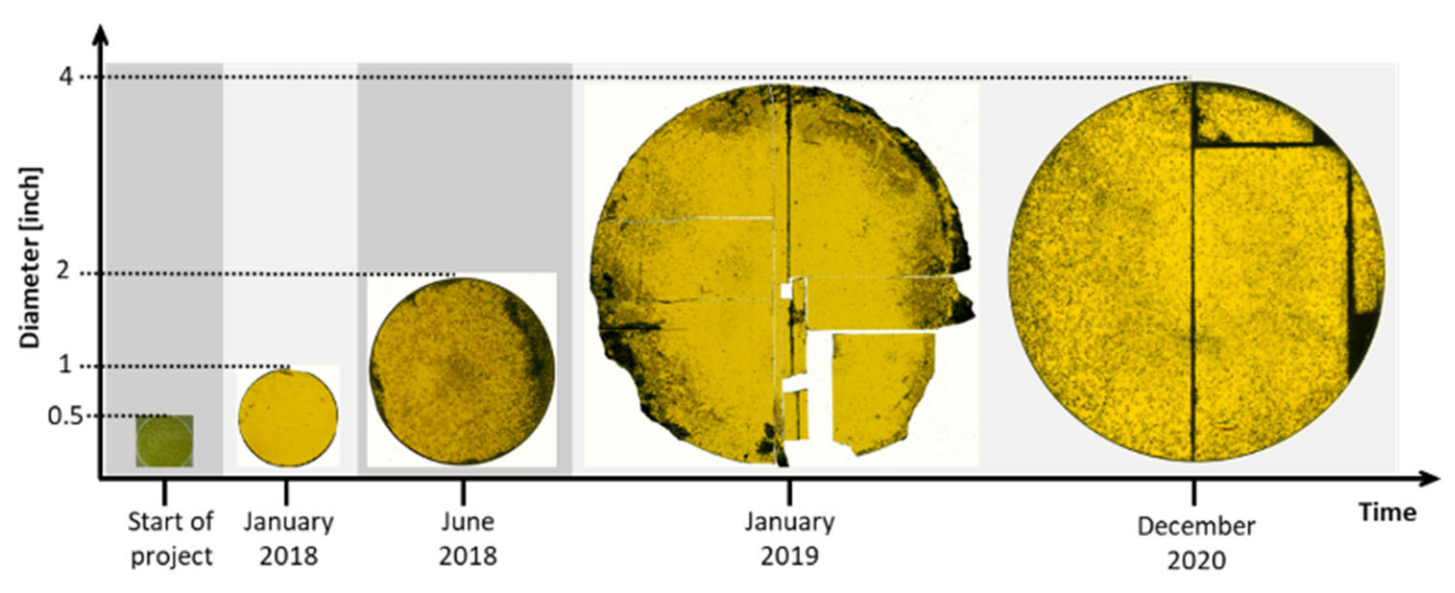
Figure 20 gives an overview of the development of the diameter of grown crystals during the project. Starting with a diameter of 0.5 inches at the beginning of the project, the first big milestone was reached in 2018 with the reproducible growth of 2-inch crystals with thicknesses of up to 870 µm. This marked the first time that bulk material, with relevant sizes, was grown regularly using a sublimation method [
26]. Such a material could be used as a seed for subsequent growth in other processes such as M-PVT or CF-PVT. With the transfer process described in
Section 2, crack-free crystals could only be obtained for up to 2 inches. For larger diameters, cracking of the thin epitaxial layer poses a problem during the preparation of the seeding stack. Nevertheless, the first growth runs on 4-inch materials were performed at the beginning of 2019. Additional improvements of the transfer process were necessary to optimize the results for the large sample size. Although the cracking problem could not be solved at this point, first-cracked but non-broken samples with a thickness of approximately 1 mm could be produced by the end of 2020, consisting of one coherent piece of crystal. Measurements of the XRD rocking curve of the full-width at half-maximum (FWHM) of the (002) reflex resulted in values of 138 and 140 arcsec for 2-inch and 4-inch materials, respectively, confirming that there is no decline in material quality for large diameters.
There are two main reasons for cracking during the manufacturing of seeding stacks. The first one is associated with the used starting material grown by CVD. Caused by a lattice mismatch between silicon and 3C-SiC of approximately 20%, a wafer bow occurs during the heteroepitaxial growth [
11]. The bow and the accompanying stress in the material will increase the probability of cracking the thin 3C layers during handling. This problem will be even bigger with increasing diameters. The second issue occurs during the etching process. During this step, NO
x species will be created [
36]. As the silicon removal starts at the edges and moves towards the center of the samples, the created NO
x species will accumulate in the middle of the sample, leading to the buoyancy of the thin remaining 3C layer. This mechanical stress will lead to cracks. For diameters up to 2 inches, this problem can be neglected but will be present for larger samples. One solution to prevent the uplift concerned the change from a horizontal to a near-vertical etching setup, reducing the effect of sample bending and therefore reducing the cracking probability. Nevertheless, micro defects induced at the edges during the laser ablation process, as well as the wafer bow, still lead to the cracking of the seeding layers.
Due to ongoing research, a new form of seeding material became available. As described by Anzalone et al. [
64], the production of freestanding 3C-SiC wafers grown homoepitaxially by CVD at elevated temperatures is possible. The availability of such seeding materials, up to a thickness of approximately 200 µm, offers new possibilities for the continuing growth using CS-PVT. Compared to the thin epitaxial seeds, no transfer process is necessary for such materials. In addition, the material grown by homoepitaxial CVD still has some setbacks concerning the wafer bow and remaining protrusion defects, and first-successful sublimation growth runs on such seeds were carried out. These experiments have proven its suitability as a seed for CS-PVT and therefore represent a promising starting point for the bulk growth of cubic silicon carbide.
Despite the appearance of different defects on the surface, all samples depicted in
Figure 20 have a bright yellow appearance typical for the cubic polytype. The results of X-ray diffraction (XRD) and Raman spectroscopy confirm the growth of 3C-SiC. The small black dots visible are associated with protrusion defects that were already present in the CVD seeding layers. These defects increase in size with the increasing layer thickness during the growth process. The darker areas at the edges of the samples were caused by both an overflow of the carbon glue during the merging step and an insufficient cleaning step afterward.
Besides the clearly visible defects, the material quality of the sublimation-grown crystal is quite high. Raman spectrometry is commonly used for the analysis of material quality as it provides a fast and non-destructive method for the evaluation of material quality. The transversal optical (TO) mode should be forbidden for defection-free (100)-oriented on-axis-grown cubic silicon carbide. However, if it is visible, it can be used to determine the stress inside the material, depending on the position of the peak [
72,
73]. For stress-free materials, the wavenumber of the peak is located at approximately 797.61 cm
−1 [
74]. An increased value is linked to comprehensive stress, whereas a lower value can be related to tensile stress. In [
26], the wavenumbers for different types of cubic silicon carbide materials were presented. It could be shown that the layers grown by CVD were tensile-stressed, caused by the lattice mismatch between silicon and 3C-SiC both for on-axis as well as off-axis materials. The value for the crystals grown by the sublimation method, with CVD materials as seeds, displayed similar stress levels. After the sublimation growth, the crystals were usually oxidized at 800 °C to remove the carbon glue and separate the samples from the polycrystalline SiC-carrier. After this treatment, the measured values for the TO mode were near the stress-free value of 797.61 cm
-1 as reported in the literature, indicating a quasi-stress-free material. In addition, XRD 2θ-ω scans were performed. For a stress-free cubic silicon carbide crystal, the in and out-of-plane lattice constant should be the same based on the cubic lattice. As stress will distort the lattice, a variation of the lattice planes will occur. The data obtained from the measurement confirm the assumption of the stress-free material after the sublimation growth and removal of the carrier. The results can be found in [
33].
Typical defects occurring in (100)-orientated 3C-SiC are stacking faults (SF), anti-phase boundaries (APB), and protrusions. To evaluate the evolution of SFs during CSPVT, KOH etching was performed. Depicted in
Figure 21 is the SF density for hetero-epitaxially grown CVD material as well as the values for sublimation-grown samples with regard to their thickness. Starting from CVD seeding materials, a defect-rich transition layer will form between the seed and the sublimation-grown material, increasing the SF density. As the CS-PVT growth will continue, this density will decrease with the increasing layer thickness. The density saturates at a level lower than the compared CVD material if the layer thickness reaches a thickness of approximately 200 µm [
75].
The characterization of the material using Raman, XRD, and KOH-etching for the evaluation of the SF density shows an improvement in the material quality for CS-PVT compared to the seeding material grown by heteroepitaxial CVD. However, the most important value regarding the real bulk growth is the thickness of the grown crystals. The limitations of the achievable thickness to this point are strongly connected to the type of defect in the material. Protrusion defects were already present in the seeding layers and have their origin in the carbonization step during CVD growth. These three-dimensional defects tended to increase with increasing layer thickness as observed by Zimbone et al. [
67] during subsequent CVD growth. In starting with such materials as a seed, a similar trend could be observed for CS-PVT [
75]. Optical images of the “as grown” surface for a set of growth runs are depicted in
Figure 22. It is clearly visible that the size of protrusions increased with the increasing layer thicknesses. At least for the investigated parameter range, this trend can be described as linear. Consequently, for even large thicknesses (d > 1 mm), the surface became more and more dominated by these defects. For bulk, growth runs with a thickness of approximately 3 mm, with a rough surface completely covered with protrusions, was observed (
Figure 22b). In addition to the ragging of the surface, polytype switches towards 6H-SiC can be observed in the crosscut depicted in
Figure 22c and can be found near or on top of protrusion defects. The edges of the defects are formed by stacking faults in the (111) planes. As these planes were equivalent to the (0001) faces in the hexagonal system, the probability for the nucleation of 6H-SiC could increase at these sides. Additionally, the growth of 6H-SiC on top of protrusion defects seems to confirm the loss of nucleation information for the continuing growth of the cubic polytype.
The reduction of protrusion density in the CVD seeding layers is an important task towards the real bulk growth using sublimation growth, especially as the material grown by CS-PVT shows a very high quality in the areas in which no protrusion defect is present. Therefore, efforts were made to reduce the protrusion density during the sublimation growth. One approach features the growth on the original transition layer from the CVD growth between the silicon and the cubic silicon carbide. Schuh et al. [
76] showed that a slight reduction of the protrusion density could be observed using this transition layer as a starting point for the sublimation growth instead of the original CVD growth front. During regular CS-PVT, a partial overgrowth of protrusion defects could also be observed, as depicted in [
77]. This effect could be observed for growth runs on on-axis seeding material as well as for 4° off-orientated-grown seeds. So far, the mechanism behind this overgrowth is not completely understood. It seems that this effect is more pronounced for off-axis-grown samples compared to on-axis grown samples.
3.16. Simulation of PVT Bulk Growth
To determine the growth conditions present inside the growth cell during the sublimation growth of 3C-SiC, numerical modeling of the temperature field and mass transport-related phenomena were performed. The basic aim was to first identify the growth conditions existing in the 50 mm apparatus and then to use such data to ensure stable growth conditions to enlarge wafer sizes of 100 mm and greater. The study examined the effect of the appropriate SiC characteristics and the various carbon materials serving as process values in the computational modeling for both the temperature profile and the associated mass transport. In order to implement the thermal field and mass transport effects, computer simulation was performed through COMSOL Multiphysics. The appropriate selection of the physical parameters related to graphite-based components, as well as for the carbon isolation characteristics over 2000 °C, appeared to not be an easy task. The main issue concerns the ambiguity, if not a complete absence of reliable data, on the temperature behavior of electrical and thermal conductivity at the growth thermal conditions.
Nonetheless, numerical modeling allows for not only the calculation of the small growth cell but also the simulation of the whole growth reactor. Besides the calculation of temperature fields, mass transport, and supersaturation, simulation with COMSOL Multiphysics provided insight into the behavior of magnetic fields as well as into the formation of hot zones.
Worthy to note, despite the fact that there is no unambiguous data on the behavior of thermal conductivity at higher temperatures for graphite crucibles and insulating components, it is possible to assert using calculations and experimental calibrations that the thermal gradient in the gas phase has no effect, unless for the second order of approximation. As a consequence, it is expected that calculating, for example, supersaturation in front of the growth interface would offer accurate findings useful for the design and optimization of growth cells.
The supersaturation of the SiC
2 gas species plays an important role, influencing the growth-limiting parameter at the seed-growth front. This supersaturation can be calculated using the partial pressure of the gas species at the seed and source. Different approaches for the calculation of the supersaturation can be found in literature, for example, by Lilov [
78] or Avrov [
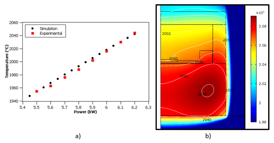
79]. Each experiment is similar in that for the calculations, the knowledge of the actual temperatures during the growth process is required. A comparison between the simulation data and the measured temperatures for the 50 mm-CS-PVT growth setup at different heating powers, showing a good agreement, is depicted in
Figure 23a. A similar trend could be observed for the 100 mm-growth cell. Additionally, an example of the temperature field present in the growth setup can be seen in
Figure 23b.
Using the temperatures obtained at the seed and source from the simulations, the supersaturations present during the sublimation growth can be calculated using the equation mentioned by Rankl et al. [
80]. They found that for the heteroepitaxial growth of 3C-SiC on (0001)-oriented 6H—SiC, a supersaturation as high as s = 0.4 is necessary to achieve a high yield. Based on the development regarding the carbon materials databases, this value was revised to s = 0.24 [
32]. In the case of homoepitaxial sublimation growth on seeds already containing the cubic polytype, a supersaturation higher than s = 0.1 was found to be suitable to ensure stable growth. It was also found that for this purpose, a source to seed a distance of 1 mm or smaller is necessary depending on the growth temperature as the supersaturation will decrease with the increasing spacing [
31].
A global model for the evaluation of the processes’ results in terms of the material growth rate can be obtained from the estimates of the mass transfer rate from the seed to the substrate once the temperature field is evaluated by the chamber simulation, as discussed in the previous section. Assuming that ballistic transport conditions occur for the Si-C molecules, which sublimate at different rates at the two interfaces, approximate estimates of the growth rate for the 3C-SiC in the different positions of the growing substrate (in a fully symmetric configuration) can be obtained from the balance between the atomic species’ effective deposition fluxes (j
dep), derived from the sources and ruled by the source temperature, and the evaporation flux (j
ev), ruled by the substrate local temperature. Due to the composition of the SiC vapor pressure, Si-rich conditions are usually assumed (see Avrov et al. [
78]) and the growth rate can be estimated by:
using the atomic carbon effective flux only. In Equation (1),
is the SiC density and
is the SiC molar mass. The expression for
and
are given by
where
and
are the source and the substrate temperatures;
and
are the molar masses of the
Si2C and
SiC2 molecules in the vapor phase; and
Ax and
Bx are the experimental parameters that rule the partial pressures of the
X species in the vapor mixtures at the thermodynamic equilibrium with the solid counterpart. Different calibrations for the partial pressures-related parameters can be found in the literature and by using the one in Reference [
78], a quantitative estimation of the growth rate in accordance with the experimental results can be obtained.
3.17. Bulk Growth by CVD
To obtain a 3C-SiC bulk material of up to 6 inches (or 8 inch in the future), a new epitaxial reactor chamber was designed and tested in several experiments. The major idea was to hetero-epitaxially grow on silicon a 3C-SiC layer and use it as seeds, melt the silicon substrate, and again start the growth at very high temperatures. Thereby, we grew a bulk substrate of 3C-SiC with a low density of SFs and low wafer bow. Most importantly, the bow can be strongly decreased since by removing silicon, the stress due to the different thermal expansion coefficients between the two materials is removed. The silicon melting provides an increase in the growth temperature and in the growth rate. In this way, thicker wafers and better crystal quality of the material can be achieved. For a better understanding of how to melt the silicon substrate, how to drain it, how to etch the remaining silicon, and how to grow the homoepitaxial layer on the 3C-SiC substrate obtained after the silicon melting, many experiments have been performed. In
Figure 24 (left), a scheme of the entire process is reported. The first two steps are the standard ones (well-reported and described in the literature).
After the melting, the SiC layer was used as a seed layer for subsequent homoepitaxial growth. [
64] In this way, growing both 100 mm and 150 mm wafers as reported in
Figure 24 (right) was possible.
The effect of temperature on the homo-epitaxial process was observed by X-ray diffraction analysis (
Figure 25). The full-width of the half-maximum on the X-ray rocking curve of the 3C-SiC (002) peak was correlated to the crystal structure and defect density (lower FWHM value means better crystal quality). The figure shows the FWHM as a function of the film thickness for several samples. The samples reported in the graph were grown in different conditions (all the samples at a low value of thickness derive from previous experiments [
6]). An increase in the film thickness has the effect of the quality of the material increasing [
81]. The initial part of the curve (from 0 to about 20 µm of thickness) shows the 3C-SiC sample’s growth with the Si substrate. For such samples, the crystal quality was limited by the presence of the silicon substrate that, starting from about 20 microns of thickness, led to cracks and extended defects. These defects are generated during the cooling down process after the growth [
6]. The three points between 60 μm and 90 μm are the 3C-SiC samples for which the silicon substrate was melted (Si fusion) and showed good crystal quality (around 200 arcsec), similar to the old 2 inch-3C-SiC wafer provided by the Hoya corporation (dotted line). These wafers were used as a template for the homoepitaxial process. The stared points (three at 200 micron) are the samples growth by using the new melting process explained in the current manuscript. They were grown at three different temperatures (1600 °C, 1640 °C, and 1700 °C). The sample grown at 1600 °C is appreciably better than the other two [
64]. The FWHM value at around 100 arcsec is very promising also compared with a thicker sample (about 400 micron) grown at a high temperature by sublimation epitaxy (PVT reactor) [
31].


 ,
, 


