1. Introduction
CdTe has established itself as the most promising material for thin film solar cell application on the market due to its direct bandgap with the value of about 1.45 eV close to the maximum of the solar spectrum the absorption coefficient of about 10
4–10
5 cm
−1 in the visual part of the solar spectrum. Recent state-of-the-art CdTe solar cell has been fabricated in the lab with the efficiency surpassing that of polycrystalline Si at over 22% [
1,
2]. Most reports about CdTe solar cells concentrate on standard test condition (STC) with the illumination intensity of 100 mW/cm
2 with a spectral distribution conforming to AM 1.5 spectrum and a cell temperature of 25 °C. However, these disagree with practical working conditions, by ignoring the case of rain, cloud, evening, morning, shade, etc., which deteriorate the irradiance intensity, so that the usefulness and applicability of the indoors’ characterization in STC of the solar cells are a controversial issue [
3]. In fact, the intensity is normally lower than 100 mW/cm
2, as confirmed by the data of the National renewable energy lab (NREL) [
4] and the short circuit current density
Jsc, the open voltage
Voc, the fill factor
FF, and the conversion efficiency
η depend on the irradiance, therefore it is essential to investigate the relationship between the diode parameters and the intensity. During previous reports about CdTe solar cells with low intensity, Randall et al. showed the comparisons of various solar cells [
5,
6], but the thorough analysis of the mechanism was missing, Shen et al. discussed the performance deviation with light irradiance in detail [
7], and the ideality factor
n and the reverse saturation current density
J0 were assumed to be constant for simplicity, the series and shunt resistances were obtained by the reciprocal of differential at points of open and short circuits in the J–V curve, which are apparently not practical. Other researchers yield average values of
n,
J0,
Rs and
Rsh ignoring influences of the irradiance [
8,
9], except the work by D. L. Batzner et al. [
10], which was mainly the comparison of different types of solar cells about key electrical feathers, although the irradiance dependence was plotted, the corresponding mechanism was not clearly demonstrated, furthermore, the extraction algorithm of
n,
J0,
Rs and
Rsh should be modified to improve the extraction accuracy. As
n and
J0 vary with the illumination intensity [
11,
12], the extraction methods of
Rs and
Rsh should also be more carefully built and selected. In this work, for CdTe solar cells, the parameter variation trends of
n,
J0,
Rs and
Rsh with illumination intensities are discussed, and the corresponding underlying mechanisms of carrier transportation and recombination are analyzed. Specifically, the cell parameters are determined from the combination of J–V curves at short circuit and open circuit within a small range of the intensities, in the way of linear fit and intersection with y axis. The data are from the CdTe module deployed on the Performance and Energy Ratings Testbed (PERT) system at the Outdoor Test Facility (OTF) [
13], named cell #1, which is fabricated mainly by close-space sublimation deposition from a developmental deposition system [
14]. The substrate is preheated to 400–600 °C, CdS is deposited with substrate temperature up to 450 °C, at a pressure of 1 Torr, and CdTe deposition follows the previous step with temperature up to 550 °C, the CdCl
2 treatment is then applied. Cell #1 was normalized to characterize a cell in this study, in order to obtain meaningful ideality factor values between 1 and 2. Cell #2 is from the fabricated device in our lab with a similar fabrication process, with glass/SnO2/CdS/CdTe as the structure. The CdS layer was formed by chemical bath deposition (CBD) technique from cadmium acetate, ammonium acetate, thiourea and deionized water, and then heat treated in a container full of N
2 with CdCl
2 at the bottom. The polycrystalline CdTe absorber layer is prepared by close-spaced sublimation (CSS) with halogen lamp as the heating source, and graphite sheet as the substrate and then heat treated with a CdCl
2 thin layer on the CdTe surface.
2. Model
The cell parameter estimation problem can be easily translated into an optimization problem, as the metaheuristic algorithms about soft computing could not guarantee consistency in computational and convergence speed, such as GA [
15,
16,
17], PSO [
18], etc., the analytical methods are thus employed because of its speed and simplicity. By omitting some minor factors, the nonlinear equation collapses to analytically solvable model, assessing the parameters directly. Among the analytical approaches, the algorithm based on two, three or more J–V curves under different levels of illumination shows good accuracy [
8,
19,
20], which is employed by us. The detail is as follow.
The ideal single-diode J–V model of a solar cell can be represented as
where
Jph and
J0 are the photon and reverse current densities, respectively,
q is elementary charge,
k is Boltzmann constant,
T is temperature in Kelvin,
n is ideality factor,
Rs and
Rsh are series and shunt resistances, respectively. From the open (
J = 0,
V =
Voc) and short (
V = 0,
J = −
JSC) circuit conditions, the following models are derived based on the assumptions of
Voc >>
JscRs and
Rsh >>
Rs [
9].
where
msc and
moc are denoted as the differentiation of Equation (1) at short and open circuit. The lines of
Voc versus ln(
Jsc −
Voc/
msc−1) and
moc−1 versus exp(−
qVOC/(
nkT)) can be fitted from the experimental values of
Voc,
Jsc and
msc−1, demonstrated later. dJ/dV at short circuit condition approximately equals the reciprocal of
Rsh.
In this study, the above algorithm was adopted, modified and generalized in the following 4 aspects for a CdTe solar cell: ① The irradiance was originally constricted to be around 100 mW/cm
2, while we expand the intensity to the range of 0–100 mW/cm
2. ②
J0,
n,
Rs and
Rsh were originally assumed to be constant, while we focus on parameter variations of a CdTe solar cell. As
J0,
n,
Rs and
Rsh vary little with small intensity range, we extract the cell parameters by dividing 0–100 mW/cm
2 into small sections. Each section corresponds to constant values of
J0,
n,
Rs and
Rsh and different sections to different values. ③ The algorithm was originally based on 5 points for linear fitting, while we consider more J–V characteristics measured for different levels of illumination, such as 9 points for linear fitting in
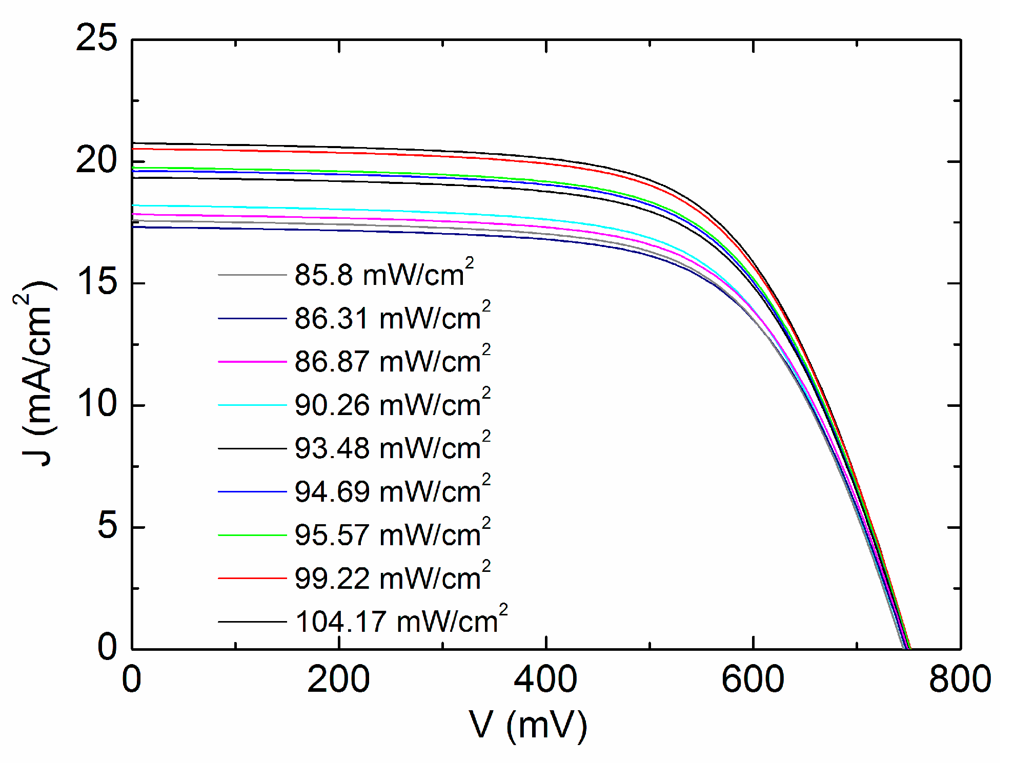
Figure 1, which apparently leads to more accurate extraction results.④ No mechanism behind the extracted parameter was investigated in the previous report, while we link them to the recombination, traps and the body resistance of a CdTe solar cell.
3. Discussion
The approach can be applied to determine the parameters during each intensity range. It is confirmed that the values of
J0 and
n should be first, obtained from (2) by plotting
Voc versus ln(
JSC–
VOC/
Rsh) from different illumination intensities. In this study, the intensity range of 85.8–104.17 mW/cm
2 for cell #1 is illustrated for instance, where
J0 and
n are considered to be constant. A total of 9 J–V curves are selected for the fitting as shown in
Figure 1, the values of
JSC,
VOC,
msc−1 and
moc−1 are obtained from J–V curves and the scatter diagram of (
JSC–VOC/
Rsh)
−1 −
moc−1 are plotted and linearly fitted, resulting in
nkT/
q through the slope and
Rs by the intersection with the y axis.
Rsh is taken to be the average value of all fitted points, and thus measured to be 199,356 Ω·cm
2.
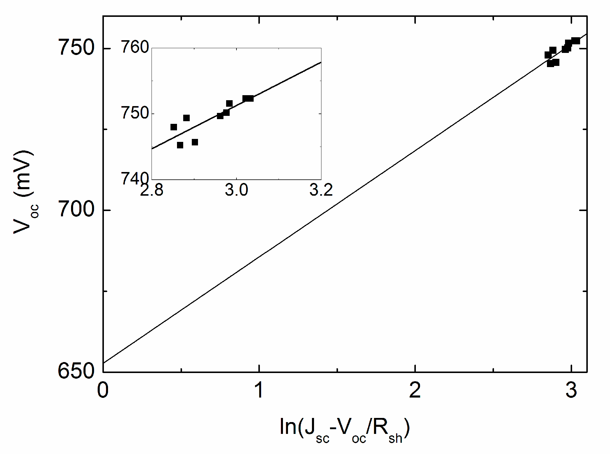
The scatter diagram of
Voc and ln(
JSC–
VOC/
Rsh) is illustrated in
Figure 2 and the original extracted data from J–V curves is described in
Table 1. It is shown that a straight line is fitted to the experimental data, with the slope and the intercept with the vertical axis confirmed, yielding
n = 0.999 and
J0 = 2.352 × 10
−9 mA/cm
2. The inset graph demonstrates the detailed data profile and the fitting line, it should be pointed out that the data appears to be diverse, nevertheless, the fitting is actually quite accurate with the corresponding maximum error less than 0.3%. Substituting the known
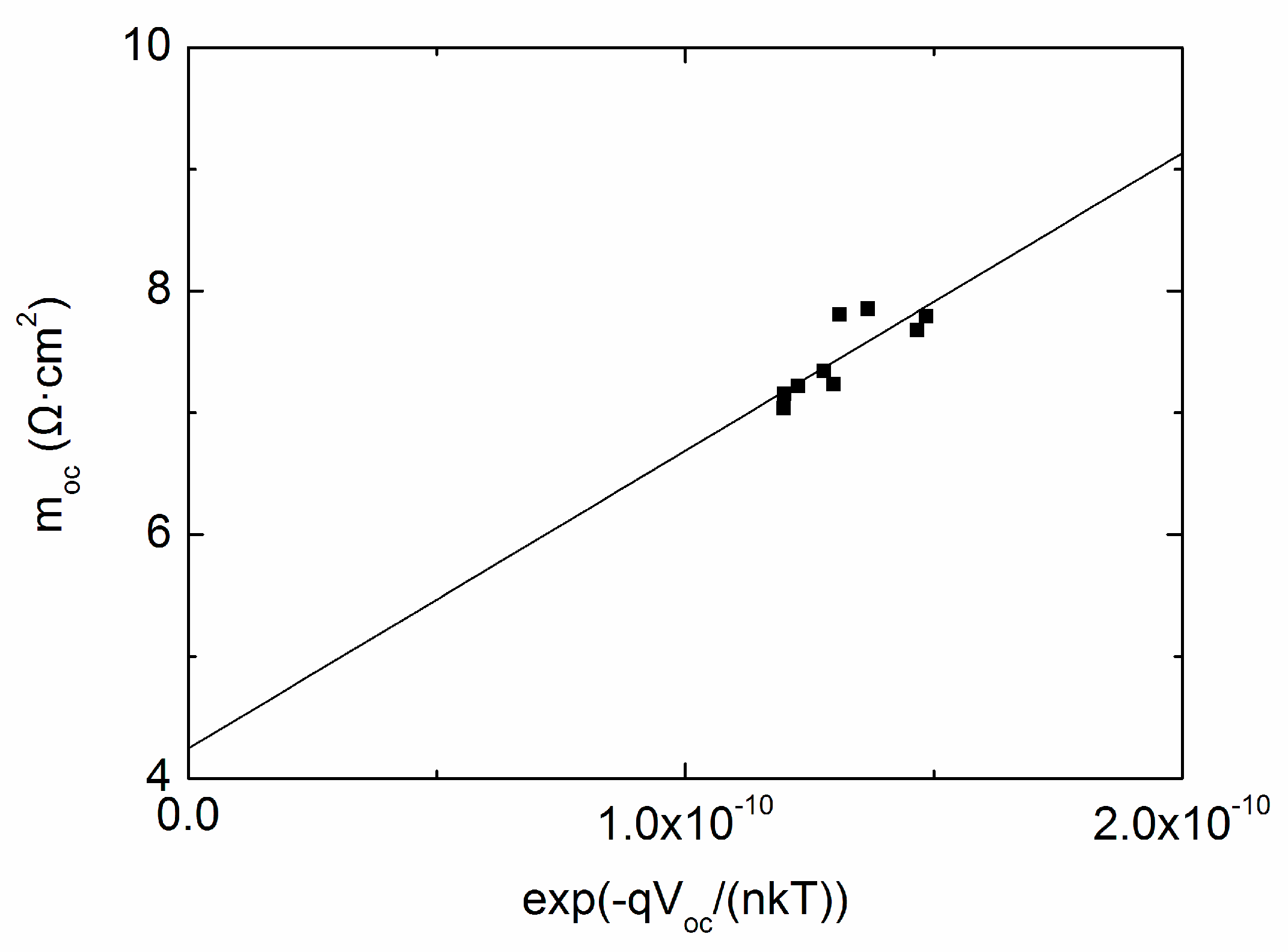
J0 and
n into Equation (3), the plot of
moc−1 versus exp(−q
Voc/(
nkT)) is illustrated as dots, and the subsequent linear fit is easily obtained as shown in
Figure 3,
Rs is determined from the line intercept with the vertical axis, which is 4.244 Ω·cm
2. The fitted values of
Rsh,
Rs,
n and
J0 are reasonably assessed to be related with the average point, meaning 92.93 mW/cm
2 for the above discussion. It should be pointed out that the fitted values correspond to the intensity range of 85.8–104.17 mW/cm
2, theoretically we are free to take arbitrary value between the range, if the same rule can be applied to other intensity ranges. Different data selection strategies lead to slightly different illumination values, but the same parameter variation trend in the whole illumination range. The average intensity approach is much smoother due to the reason that sometimes the testing points are not uniformly distributed. The “middle-point selection” strategy may cause parameter surge, which is explained in detail later in shunt resistance discussion.
Repeat the extraction operation under other low intensity conditions, a number of similar fitting lines are obtained at 76.16 mW/cm
2, 63.36 mW/cm
2, 46.38 mW/cm
2, 32.03 mW/cm
2 and 14.64 mW/cm
2. It should be pointed out that the variations of the diode parameters for the irradiance lower than 20 mW/cm
2, is partially due to the irradiance and current measurement uncertainty, as the uncertainty is relatively large under that case. In order to accurately extract
n,
J0 and
Rs at 14.64 mW/cm
2, we take the largest intensity range to reduce the effect of measurement uncertainty. Finally, all parameters are extracted and listed below in
Table 2.
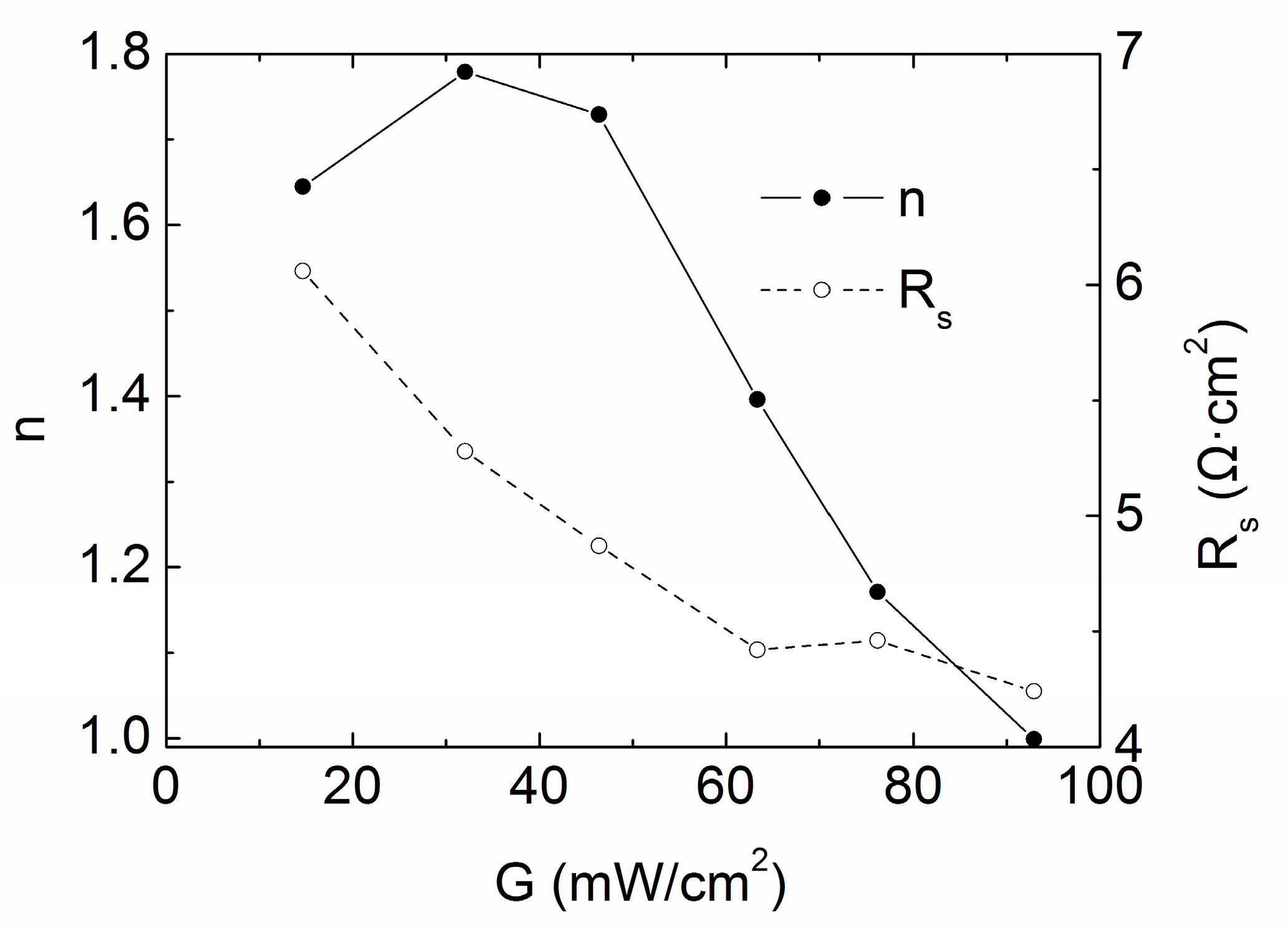
Figure 4 shows the variations of the ideality factor
n and the series resistance
Rs with low solar irradiance, the former is apparently governed by recombination including bulk recombination, surface recombination and space-charge recombination, the latter is caused by bulk property and geometry. The ideality factor
n under the standard illumination is approaching 1, indicating a nearly ideal diode, the rise in
n with the decrease of intensity is physically suggesting a partial shift in the forward current mechanism from asymmetric recombination near the metallurgical junction, to more symmetric recombination distribution over the depletion region [
21]. Therefore, the space charge recombination is more contributive at low intensities; the variation of
n is attributed to the bulk and surface recombination mechanisms at high intensities. For
Rs of cell #1, it ranges between 4.24–6.06 Ω·cm
2, denoting weak parasitic effect. As the light intensity goes down, the slight decrease of
Rs between 60–80 mW/cm
2 is maybe for test deviations—or probably due to the slight decline of surface temperature, although fixed to be constant. The sharp rise of
Rs below 60 mW/cm
2 is because of reduced carriers in the absorption layer. Specifically, the photo-generated carriers decline and the body resistance of CdTe absorption layer rise, while CdTe layer makes a major contribution to the variation of series resistance of the whole cell, therefore
Rs increases.
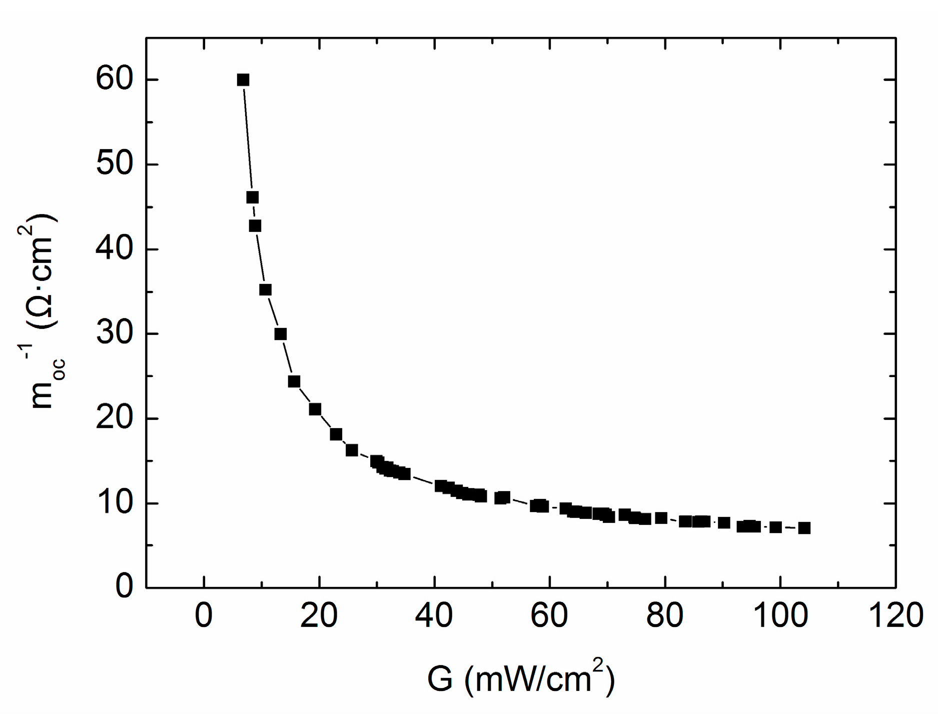
Next
moc−1 as a function of the irradiation intensity
G is considered, as shown in
Figure 5 with 54 points as the tested values. It is seen that with the decrease of
G,
moc−1 rises exponentially. If we approximately regard
moc−1 to be
Rs, the curve in
Figure 5 is consistent with our traditional intuition of
Rs versus
G and is exactly the same as the report of Shen [
7]. But the true deviation of
Rs is much smoother, according to our result in
Figure 4, and sometimes the slight drop of true
Rs can be found even with the decreased illumination intensity.
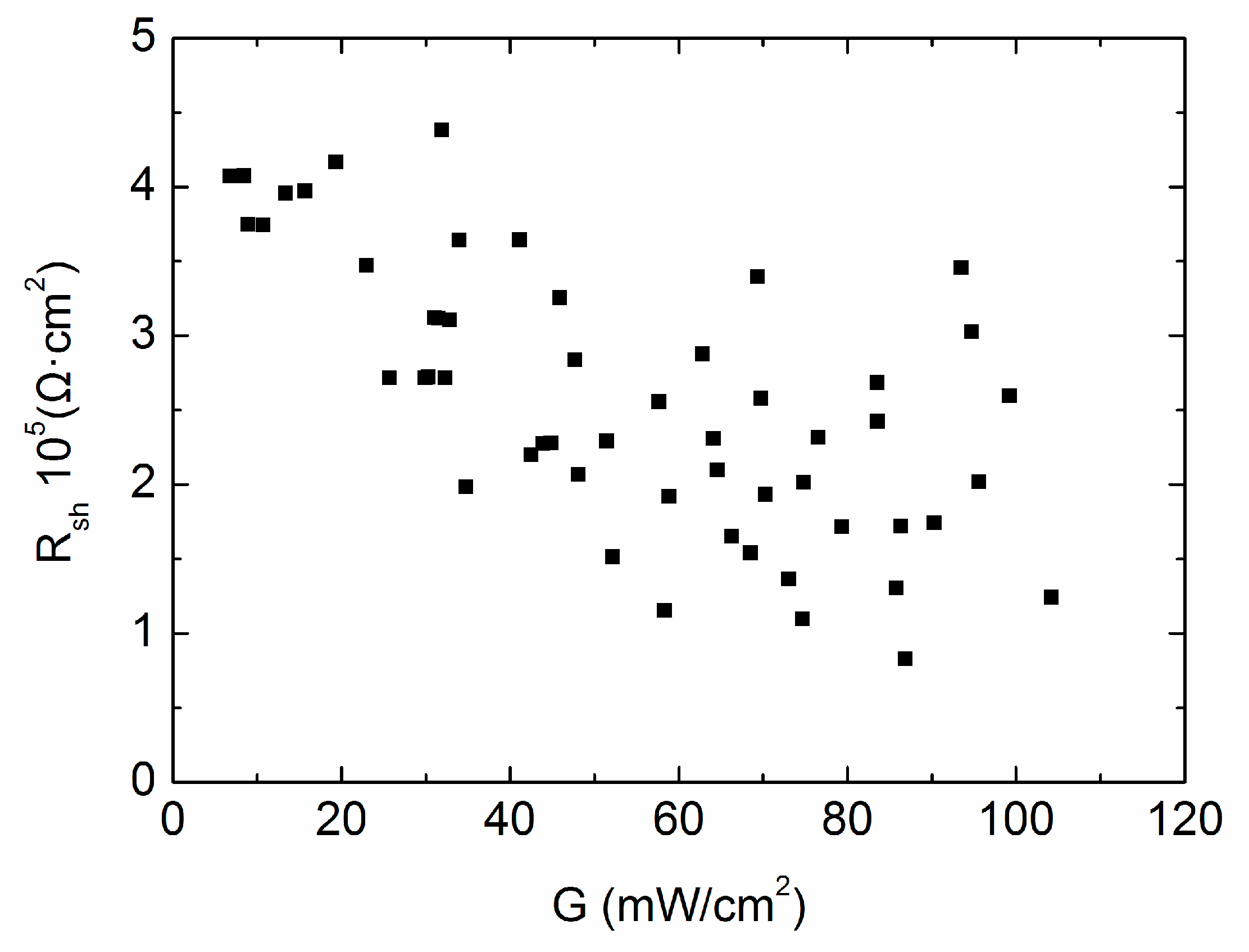
Figure 6 demonstrates 54 shunt resistance values from all experimental J–V data, by differentiating J–V curves at short circuit and then making a reciprocal transformation. Apparently, the shunt resistance exhibits poor stability. If we take the “middle point selection” strategy representing every 9 fitting points to determine
Rsh, for example,
Rsh at 93.48 mW/cm
2 denotes the shunt resistance at 104.17 mW/cm
2, 99.22 mW/cm
2, 95.57 mW/cm
2, 94.69 mW/cm
2, 93.48 mW/cm
2, 90.26 mW/cm
2, 86.87 mW/cm
2, 86.31 mW/cm
2 and 85.8 mW/cm
2, it probably causes
Rsh to oscillate up and down within the whole intensity range, while it is far from the truth. If we take an average value of every 9 points to smooth the
Rsh deviation, a clear monotonous increase of
Rsh can be seen with the decrease of
G, as shown in
Figure 7.
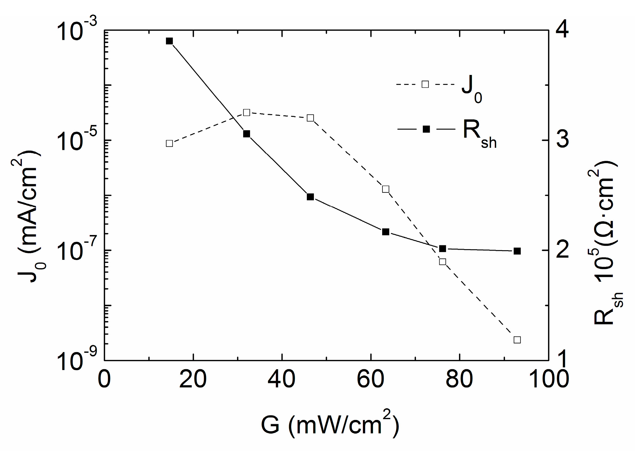
Figure 7 shows the variations of the shunt resistance
Rsh and the reverse saturation current density
J0 with low solar irradiance.
Rsh exceeds 100,000 Ω·cm
−2, the defect caused current model should be employed to explain the variations,
Rsh is so high that the cell is well designed. With a decreased light intensity, the photo-generated carriers and hence the captured carriers also decreases, indicating the increase of
Rsh [
22].
The reverse saturation current density relies on space charge recombination, bulk recombination, and surface recombination. The principles are as follows: (1) If the light intensity is low, the space charge recombination is significant, and the reverse saturation current density is large; (2) If the light intensity approaches 1 sun, the main contribution is from the bulk recombination and the surface recombination, and the corresponding current density is thus relatively low; (3) Less generation of carriers causes
J0 to drop. Therefore,
J0 monotonously increases with the irradiation intensity decreasing from about 1 sun to 30 mW/cm
2, as recombination mechanisms dominate
J0. With the light intensity lower than 30 mW/cm
2, principles (1) and (3) take effect. When the two contributions are balanced,
J0 keeps nearly constant, when principle (3) overlaps (1), the cell starts to cut
J0. It is also the reason that
n in
Figure 5 reduces its value below 30 mW/cm
2.
Next the cell with relatively low Rsh is investigated. The J–V curve measurements under low irradiance intensities are carried out by a 3-A solar simulator (Crowntech) and Keithley 2400. The following figures are the data extracted by the same approach.
From
Figure 8, it is seen that the shunt resistance is 10 times lower than that of cell #1, the traps plays a more significant role than that of cell #1. For cell #2, with the decrease of the irradiance intensity, the captured carriers decreases due to the decreased photo-generated carriers, leading to the increase of the shunt resistance, showing an exponential tendency. The reverse saturation current density is continuously cut down due to the non-stop shifting from symmetric recombination to asymmetric recombination, which is quite different from that of cell #1.
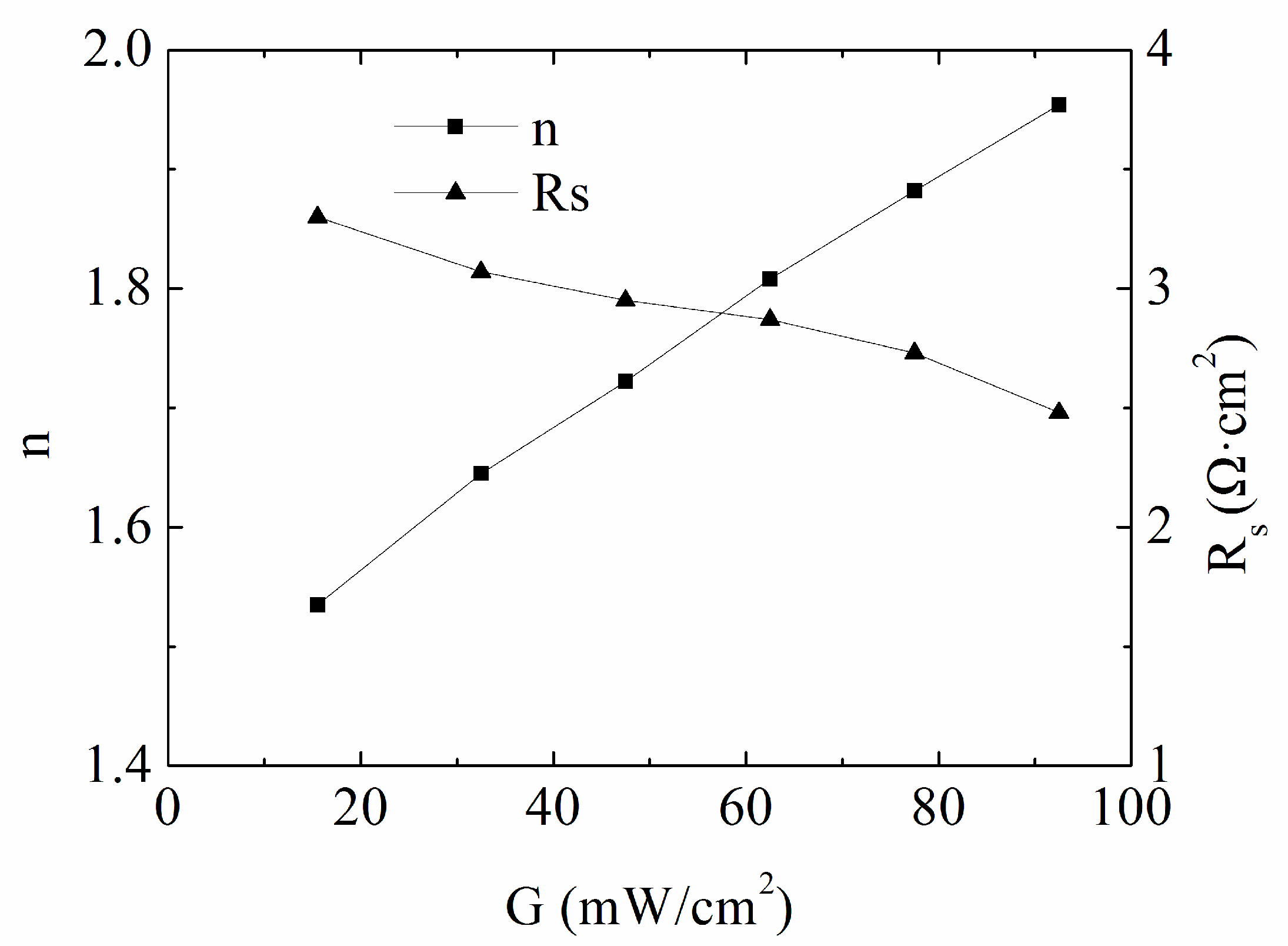
From
Figure 9, the ideality factor is nearly 2 under standard irradiation condition, and drops to 1.535 with the light intensity of 17.3 mW/cm
2, indicating the same recombination mechanism as that of the reverse saturation current density. The parasitic effect is weak with the series resistance of 2.48–3.3 Ω·cm
2, also showing a well-fabricated cell. The carrier number lowers with decreased light intensity, resulting in a slight rise of the bulk resistance, and hence, the series resistance is on the increase.
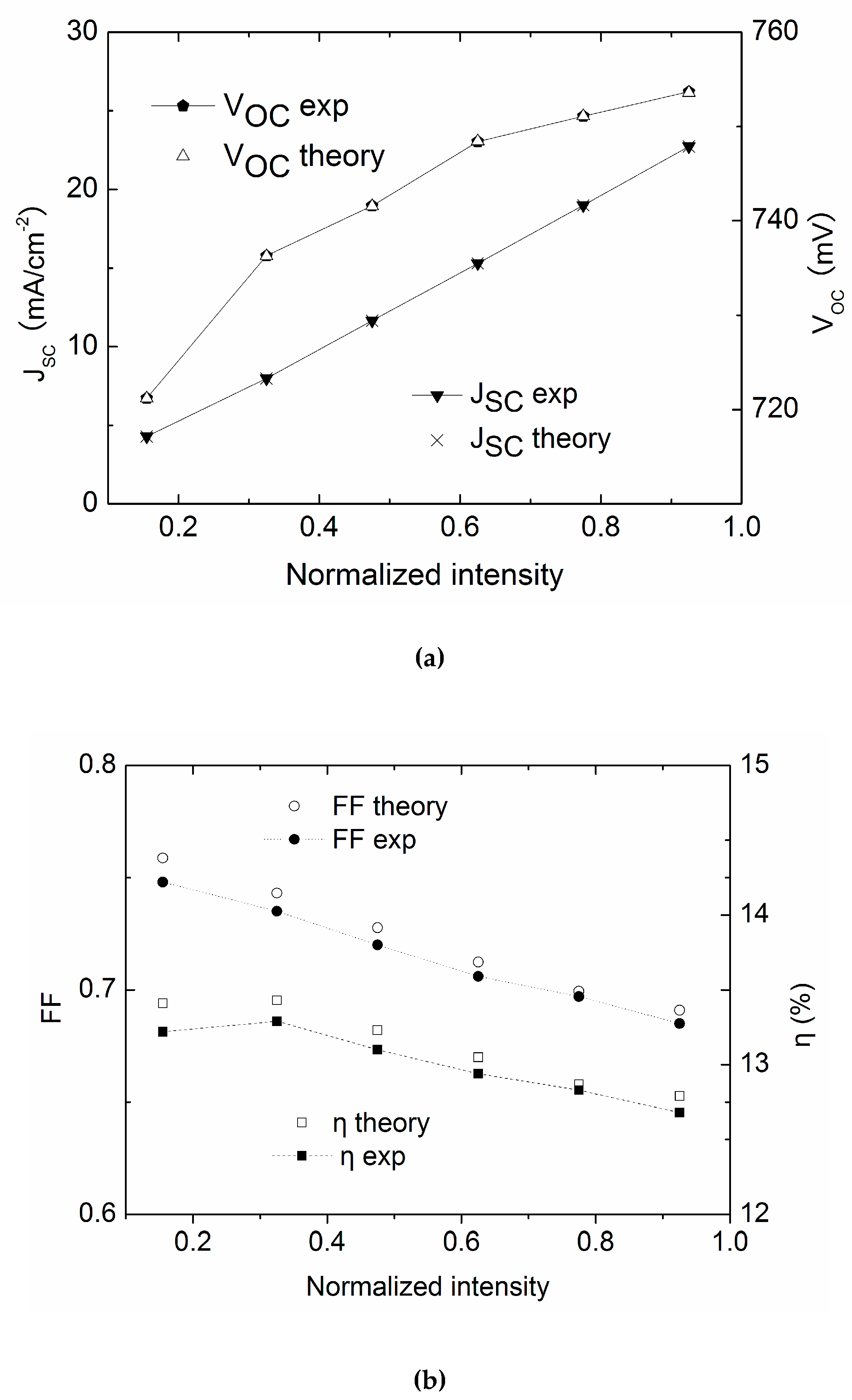
In order to verify the algorithm, the extracted parameters are substituted into the one-diode model, thus obtaining theoretical values of
Voc,
Jsc,
FF and
η. The values are then compared with the experimental data, as shown in
Figure 10a,b. Apparently, the deviations are minor, verifying the validity of the modified method.


