Article

Adaptation of Microinverter Reference Design for Integration with Battery Energy Storage Systems in Microgrids

Faculty of Electrical Engineering, Mechanical Engineering and Naval Architecture, University of Split, Ruđera Boškovića 32, 21000 Split, Croatia
*
Author to whom correspondence should be addressed.
Energies 2024, 17(6), 1487; https://doi.org/10.3390/en17061487
Submission received: 8 February 2024 / Revised: 8 March 2024 / Accepted: 18 March 2024 / Published: 20 March 2024
(This article belongs to the Collection Renewable Energy and Energy Storage Systems)

Abstract

:
The paper presents an adaptation of the microinverter platform from Texas Instruments to incorporate a battery energy storage system (BESS) alongside the development of the BESS system itself. Initially designed for unidirectional power flow between PV panels and an electric grid, the platform required modifications to accommodate bidirectional energy transfer for BESS integration. These modifications encompass software adjustments and hardware enhancements, which are all detailed within the paper. The electrical configuration includes selecting and deploying components such as DCDC power converters, microcontrollers, measured signals, and actuating signals to facilitate battery connection to the platform’s DC bus. Furthermore, a supervisory control and data acquisition (SCADA) system is devised for supervisory control and monitoring, with its implementation outlined. Control software tailored for the chosen microcontroller of the DCDC converters is described in terms of structure and functionality. A hardware-in-the-loop (HIL) methodology is employed to validate the proposed modifications and microgrid configuration. Utilizing the real-time simulator OPAL-RT, the paper presents experimental results and their analysis within the considered microgrid environment.

1. Introduction

In the current climate change landscape, there is a global shift toward replacing traditional, nonrenewable energy sources with sustainable alternatives such as wind and solar power. Microgrids have emerged as a critical solution to efficiently integrate these distributed renewable energy sources into consumer networks within the centralized utility grid. Advancements in policy frameworks and technological innovations now empower communities and businesses to establish microgrids, thereby enabling localized energy production and consumption.
Microgrids offer several significant advantages, including reducing carbon dioxide emissions and increasing energy efficiency, thus leading to notable energy savings. Moreover, microgrids provide a reliable power source to communities, particularly when access to energy from the centralized grid is disrupted.
Integrating photovoltaic (PV) panels into low-voltage networks can pose challenges, notably overvoltages and network overloads. However, microgrids equipped with battery energy storage systems (BESSs) offer a solution to mitigate this issue. The BESS plays a crucial role in regulating the power output from PV panels, thereby addressing overvoltage concerns. As highlighted in [1], a temporary measure to manage overvoltage is imposing limits on the maximum number of PV panels connected to a specific grid connection point.
Microgrids have traditionally been associated with AC electric networks. However, the emergence of renewable energy sources and storage systems, such as PV panels and batteries, which generate DC currents, has sparked a growing interest in DC microgrids [2].
The benefit of these networks is that they do not require synchronization and frequency regulation. The loads connected to the traditional AC grid usually require DC voltage from the AC grid using rectifiers. These additional conversions reduce the efficiency of the overall energy system. Connecting the loads directly to the DC grid increases efficiency [3]. While control systems for AC grids are well-established and standardized due to their extensive use over many years, the landscape is different for DC networks, thus necessitating a distinct approach.
Today’s microgrid topologies used to realize it are single bus, radial, ring, mesh, and interconnected. At the same time, two configurations are used today for single bus topology: unipolar configuration [4] and bipolar configuration [5,6,7,8,9,10,11]. In the unipolar configuration, there are only active potential U D C and ground, while in the bipolar configuration, there are two potentials with the same value but opposite sign and ground. For all of these today-used topologies, the problem arises from their control and coordination between their microgrid elements.
The communication between elements in the microgrid is crucial because it is needed to coordinate work between all its components. However, what will happen with the microgrid if this communication line fault arises? One of the solutions that Shahid M. U. et al. [3] propose is to use a method to detect this fault and bring the microgrid to regular operation while this fault is not eliminated. This proposed method has only been verified by simulation.
Thounthong P. et al. present the adaptive Hamiltonian PI controller to achieve DC bus stabilization and current sharing for the fuel cell boost converter [4]. Mathematica and MATLAB/Simulink were used to test stability and robustness, and experimental verification was conducted. This paper has focused on the element of the microgrid and its control.
Xu L. and Chen D. both proposed hierarchical control strategies, with Xu [12] focusing on power balancing and fault management and Chen [13] on voltage control and stability.
Pires V. F. et al. [5] review the multiple architectures and topologies of power electronics, which are proposed to solve the problem of voltage and current imbalances due to the sources and loads being unequally distributed within the microgrid.
In their research, Prabhakaran P. and colleagues [6] presented a DCDC converter connecting PV panels and fuel cell sources to a low-voltage bipolar microgrid. They proposed a topology that is highly efficient, compact, and one-directional. The converter maintains the maximum power point of the PV source and regulates the voltage of one pole. It can also be used to connect two types of microgrid configurations.
Guo C. et al. [7] proposed a control topology for a radial multinode bipolar DC distribution network. This topology includes primary and secondary control, as well as voltage balancers. The proposed control was validated through simulation using MATLAB/Simulink. The study compared their control with traditional droop control [14], which is a typical decentralized control method that relies on a linear relation with the current that produces the voltage droop.
In a bipolar DC microgrid, unevenly distributed loads can cause a voltage balancing issue. To address this problem, H. Doubabi et al. [8] proposed an advanced control strategy that uses a backstepping method called the voltage-balancing controller. This approach guarantees global asymptotic stability and robustness. The controller parameters were determined using a particle swarm optimization algorithm, and the simulation was conducted in MATLAB/Simulink to verify its effectiveness.
In their paper, Sepulveda-Garcia et al. [9] put forth a novel approach towards analyzing the power flow in bipolar DC microgrids. The method considers the presence of unbalanced loads and neutral potential, which are often observed in practical systems. In order to solve the power flow equations, the authors employed Taylor series expansion with linear terms, which is an effective technique for approximating nonlinear functions. This approach enables accurate assessment of the power flow in a bipolar DC microgrid, which is essential for ensuring optimal operation and stability of the system. Overall, the proposed method contributes to advancing the understanding of power flow analysis in DC microgrids and has the potential to facilitate the design and operation of such systems in various applications.
This paper presents a detailed proposal for modifying the platform based on a Texas Instruments reference design to integrate a battery energy storage system (BESS) with its DC bus using a single-bus topology and supervisory control mechanisms. The proposed modifications aim to enable bidirectional energy transfer between the BESS and the electric grid, which was impossible with the platform’s initial unidirectional energy flow design.
The hardware and software modifications required are outlined in the paper, including implementing supervisory control mechanisms and adjusting the control algorithm of the DCDC converter. The DCDC converter is responsible for regulating the voltage output of the BESS and must be tailored for integration into the platform’s DC bus. However, as the DCDC converter is controlled by a separate digital signal processor (DSP), it requires more direct communication channels with other microgrid elements, thus complicating the overall system operation adjustment. Therefore, the proposed modifications consider all error situations and aim to simplify the system operation.
A hardware-in-the-loop (HIL) simulation is used to test and analyze the results to validate the proposed modifications. The HIL simulation will simulate the microgrid in a controlled environment to ensure the system operates as intended and identify any potential errors. The paper also describes the SCADA system for controlling all the microgrid elements, which is an essential component of the proposed modifications.
The paper comes to an end by presenting the results of the proposed modifications and analyzing the results. The results show that the proposed modifications effectively enable bidirectional energy transfer and improve the microgrid’s overall performance. The proposed modifications are essential for integrating the BESS with the platform and can be used as a reference for similar modifications in other microgrid systems.

2. System Description

Figure 1 shows the microgrid established within the Faculty of Electrical Engineering and Naval Technology laboratory in Split. This microgrid has been set up to demonstrate the functioning of various components that are integral to a typical microgrid.
The microgrid consists of three key elements: a photovoltaic (PV) panel, battery energy storage systems (BESSs) consisting of batteries, and an electrical grid. These components are connected through a DC bus, which helps dampen the system’s transient dynamics.
To connect the PV panels to the DC bus, a DCDC converter is required due to the difference in voltage levels between the two. Furthermore, a one-phase grid-forming converter connects the DC bus to the network. This setup, which consists of the PV panel’s DCDC converter and the one-phase grid-forming converter, has been realized using the TMDSSOLARUINVKIT platform (shown in Figure 1) from Texas Instruments, Dallas, TX, USA, which provides a reliable and efficient solution for the microgrid.
However, it is essential to note that the energy flow in this platform can only be in one direction—from the PV panel to the electrical grid. This means that modifications are required to use this platform in the microgrid shown in Figure 1, which has batteries connected to the DC bus. The necessary modifications have been made to the platform’s control algorithm and hardware to enable it to function as required in the microgrid.
PV panels convert energy from photo energy, which is carried by a single photon, to electric energy, which is carried by electrons and positive ions in electrical wires. These PV panels can be connected in different ways. They can be connected in series to a central DCDC converter. This converter type works at higher voltages, around 400 and 600 V. Alternatively, every PV panel can be connected with their own DCDC converter to the DC bus. Because the voltages of these connected PV panels do not exceed 80 V, safety measures can easily be satisfied according to the PV panels connected in series. However, this connection type is costly. On the input of the DCDC converter of the platform, PV panels with voltages between 25 V and 40 V can be connected. The maximum power of the connected PV panel is 280 W for a grid voltage of 220 VRMS.
A DCDC converter becomes imperative due to voltage disparities to establish a connection between batteries and the DC bus. This converter facilitates bidirectional energy flow, thus allowing energy to move in two directions. Specifically, energy can flow from the batteries into the DC bus, accumulating in the DC bus capacitors, or from the DC bus back to the batteries. Additionally, surplus electric energy stored in the capacitors necessitates transfer to the electric grid, which is a task effectively carried out by the grid-forming converter. The DCDC converter responsible for managing battery power is implemented using a half bridge configuration.
A physical separation is needed between the DCDC converters of the batteries and the DC bus, because the DCDC converter can operate only when the overall voltage of the batteries connected in the series topology is much smaller than the DC bus voltage. If the voltage of the batteries exceeds the voltage of the DC bus, there will be uncontrolled energy flow from the batteries to the DC bus. This could lead to a short circuit when the DC bus is discharged. An electromechanical relay is used to physically separate the DCDC converters of the batteries from the DC bus.
Another physical separation in this circuit is between the grid-forming converter and the electrical grid. This separation is needed when the microgrid works in island mode. Alternatively, it is needed when the DC bus needs to be discharged entirely, i.e., when all sources and loads of the microgrid will be shut down.
The control algorithms of these converters are implemented in a microcontroller F28035, which has C28x digital signal processors (DSPs). The frequency of this CPU at which it works is 150 MHz. One microcontroller is used for converters of the platform, and the second one is used to control four DCDC converters for connecting four packs of batteries, which have a voltage of 200 V, to the DC bus, which operates at a voltage of 388 V. These microprocessors have all the needed peripheral elements for controlling these converters. These elements are analogue–digital converters (ADC), pulsewide modulation (PWM), and general purpose digital input/output (GPIO).
In three different operating modes [15] shown in Figure 1, the microgrid needs to operate as follows: B2G (blue line), B2B (green line), P2B (red line), and P2G (red line). One direction flow is in the P2B and P2G operating modes, while duplex energy flow is in the B2G and B2B operation modes. In the B2G mode operation, the electric energy is transferred from the batteries to the electric grid; in the B2B, the energy is transferred from one battery to the second battery, while in the G2B mode operation, the energy is transferred from the grid to the battery. The B2B mode is used to ensure that all batteries of the BESS are equally charged. These modes of operation are the marginal operating modes. At the same time, the combined operating modes can also be, e.g., the G2B and B2B. In this combined mode of operation, the battery is charged from the grid while there is simultaneous voltage balancing of the batteries. The control loops must consider all of these and always bring the microgrid to equilibrium.

3. Modeling and Control Loops

The higher control loops are shown in Figure 2. The microgrid’s battery energy storage system (BESS) comprises four batteries interconnected via DCDC buck–boost converters. These converters are realized using a half bridge, which uses MOSFET transistors for switching. Control pulses are generated from the current controller, which maintains the current value of the battery. Because the voltage on the DC bus is maintained, the battery’s power is proportional to this current value. Four current controllers are implemented within one microcontroller, F28035, which maintains the current value defined with the current reference value. The SCADA system, which runs on a Linux computer, changes this reference value. Together with the current controller, there is a microcontroller-implemented supervision control that defines the state in which the batteries are momentarily and the safety measures.
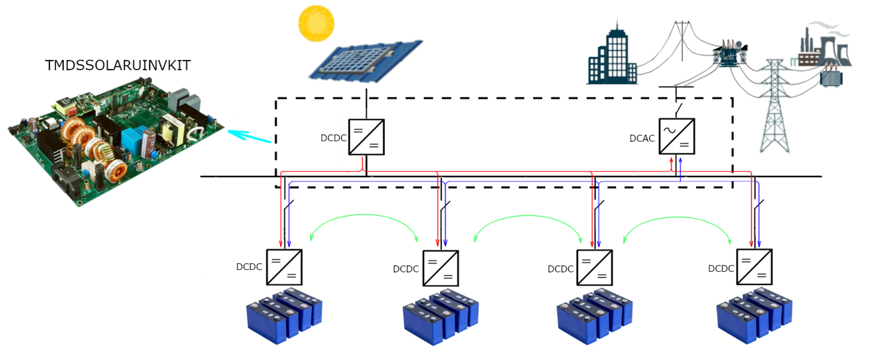
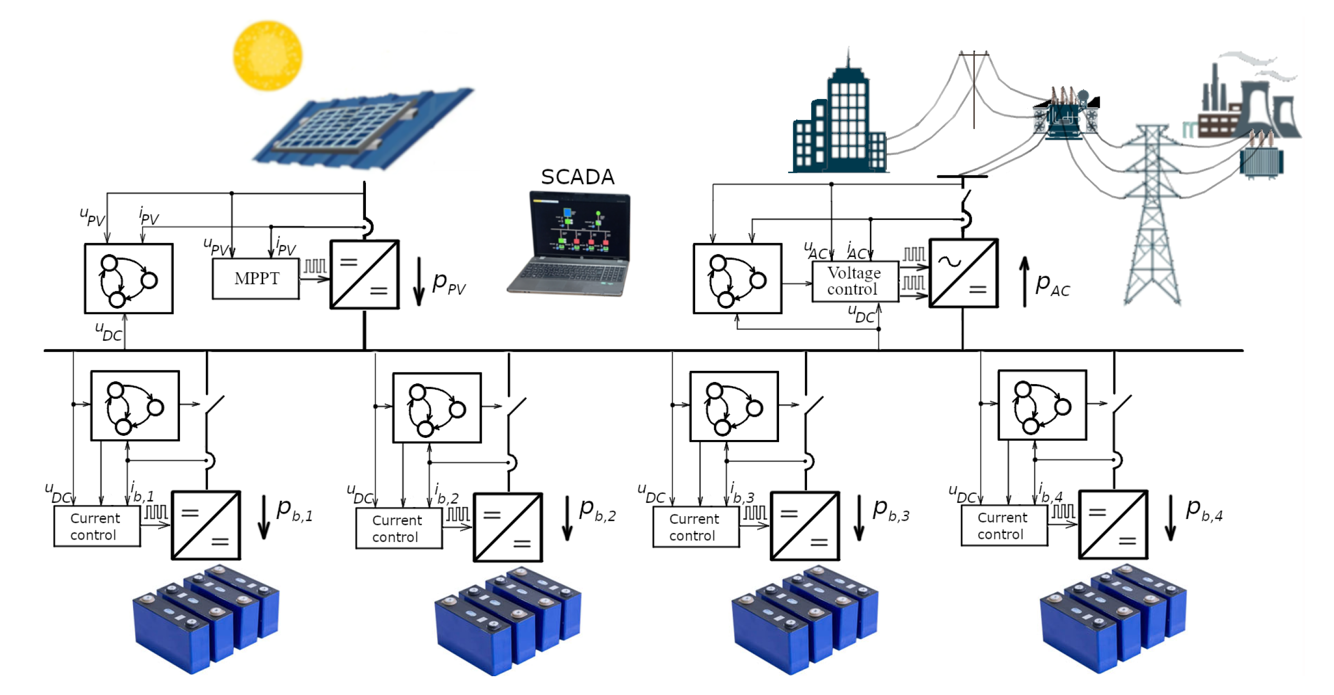
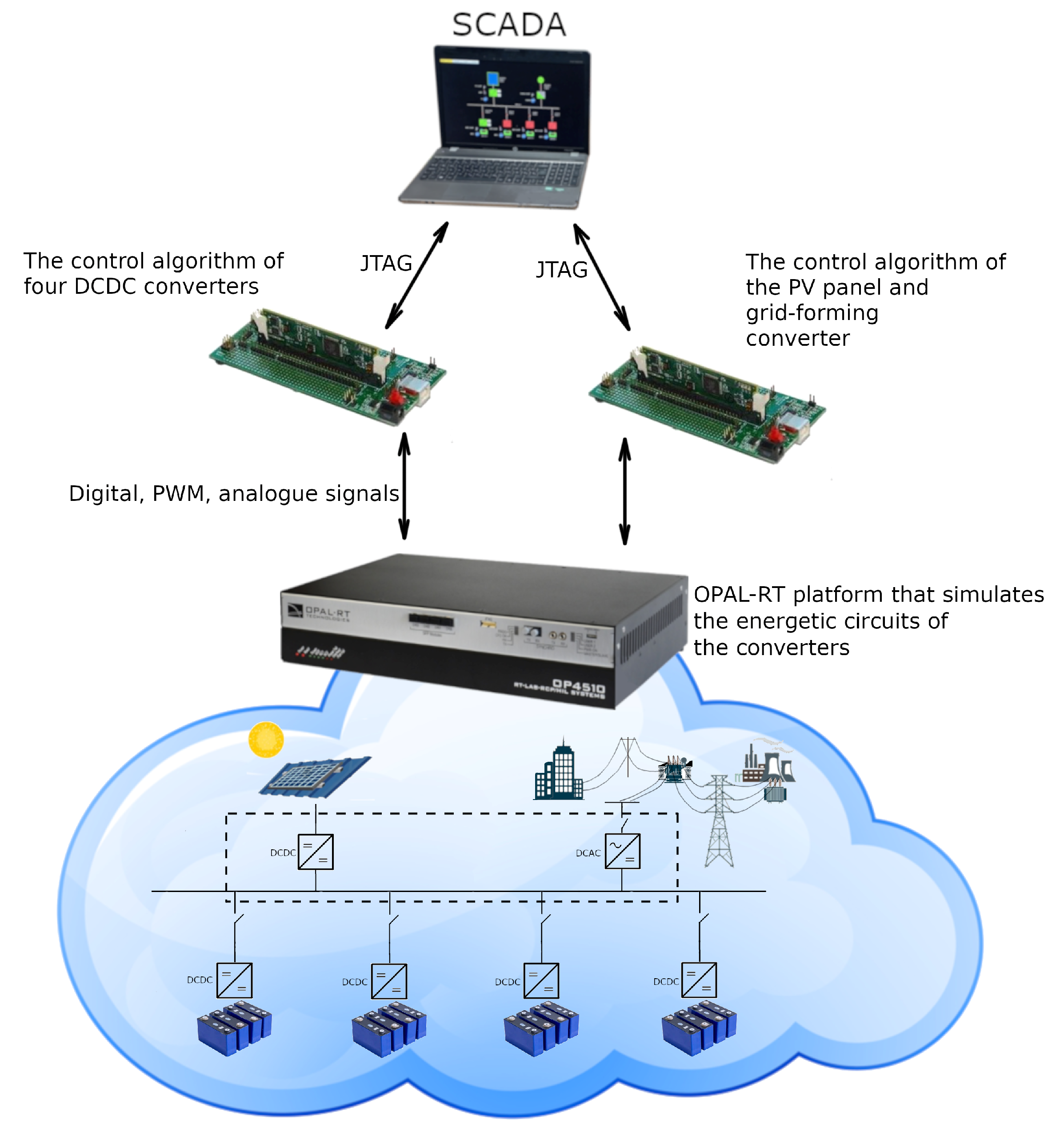
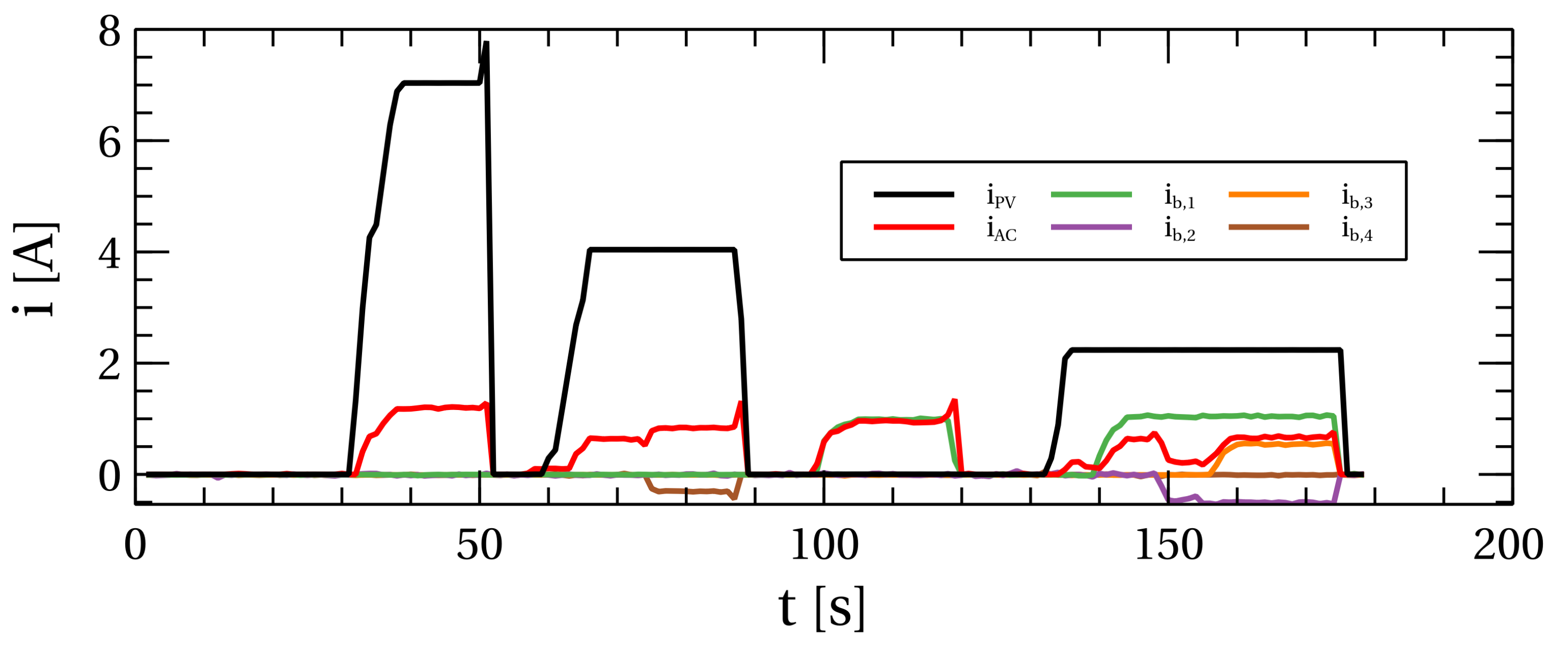
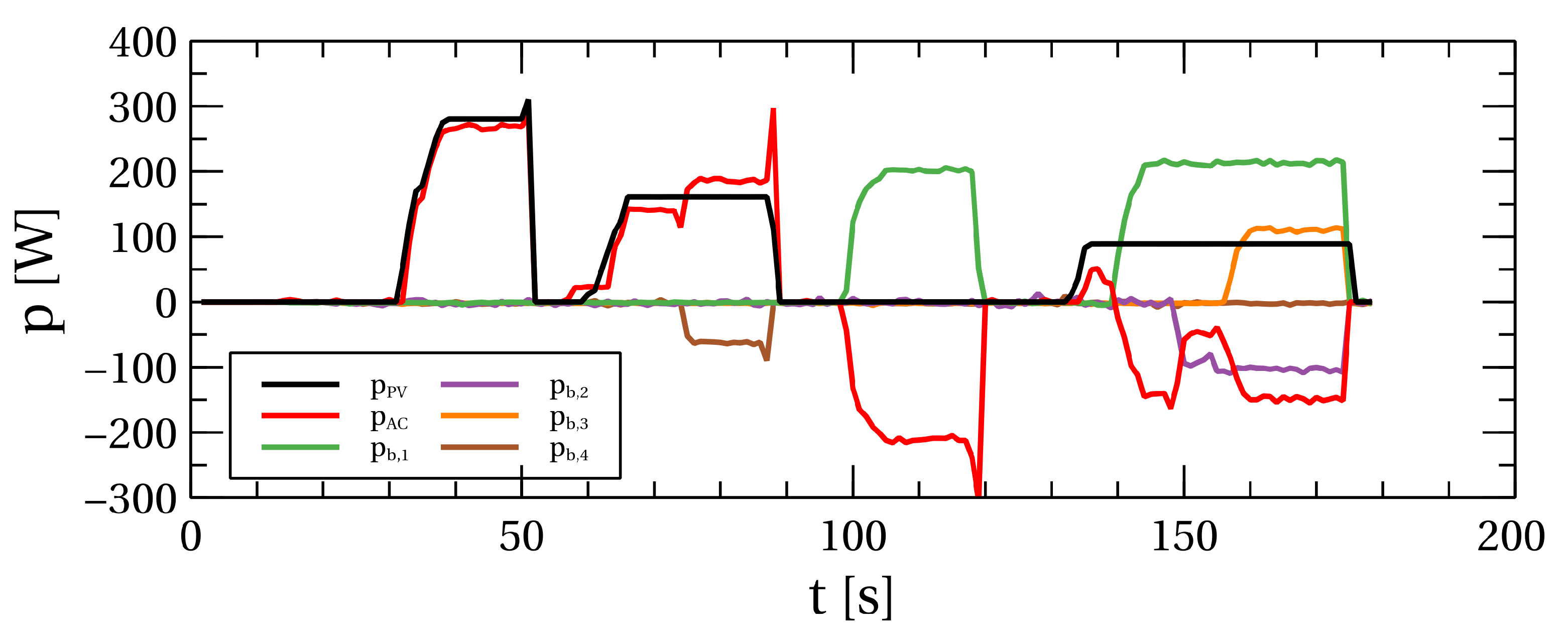
Adjusting the voltage level is essential for connecting the PV panel to the DC bus, as PV panels typically operate at voltage levels around 30 V. Because the grid-forming converter of the platform is not galvanically separated from the electric grid, it is needed to galvanically separate the PV panel from the DC bus, which is done by using a flyback converter. With this, the PV panels can be grounded, which is needed in practice. The maximum energy production from the PV panels is accomplished using the MPPT algorithm, because they are voltage-controlled current sources. This algorithm changes the PV panel voltage, which is changed by using the current controller to achieve the maximum PV panel power production. Additionally, a supervisory control algorithm is employed to adapt the settings of the MPPT algorithm and the current controller based on the microgrid’s state, thereby ensuring compliance with safety measures.
The control algorithm can be easily applied to large-scale systems with no modification, wherein it only requires changes to the parameters in the configuration file of the controllers and protection system. However, hardware changes will be necessary if higher-power PV panels or batteries are used, particularly in the power switches.
The microgrid is connected to the centralized utility, an AC grid, using a grid-forming converter. This converter is a one-phase converter, which transfers energy from the DC bus to the AC network. The main control algorithm consists of the voltage controller, which maintains the accumulated energy in the capacitors connected to the DC bus. In this way, depending on the voltage value of the DC bus, the controller will generate pulses to give energy to the AC grid or to obtain energy from the AC grid. For this control algorithm to work, it needs to measure the voltage of the AC grid to generate the sine current in phase with the voltage. Like the control algorithm of the PV panel and DCDC converters of the batteries, this control algorithm also has a supervision control algorithm for changing the configuration of the subordinate algorithm and satisfying the safety measures.
In this work, we have meticulously outlined the supervisory control system of the microgrid, thereby utilizing state diagrams to elaborate the operational dynamics of each element. The coordination between these elements is achieved by using the process value, which is the DC bus voltage, as there is no direct communication between the processors of the DCDC converters and the inverter. Even though the control algorithm of the flyback converter and the inverter are implemented in the same processor, the two algorithms are kept separate, so they do not exchange information. For a comprehensive understanding of how this coordination is meticulously achieved, we have provided detailed insights in Section 3.1, Section 3.2 and Section 3.3, where the state diagrams offer a depiction of the control dynamics.

3.1. Flyback Converter

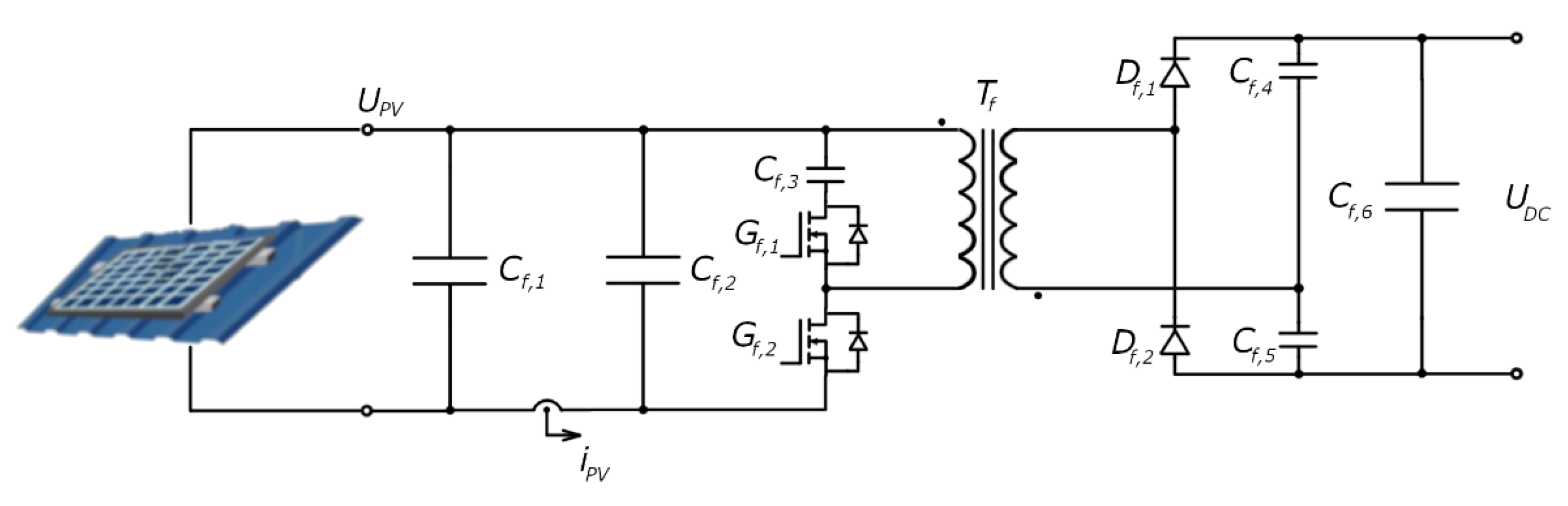
The more advanced version of the flyback converter, which has the additional components, is shown in Figure 3. Its parameters are given in Table 1. To reduce the voltage stress of the MOSFET G f , 2 when switched off, an additional MOSFET is used with the capacitor C f , 3 to discharge the magnetic energy of the flyback transformer T f . This accumulated energy in the capacitor C f , 3 is transferred back to the secondary circuit of the flyback transformer when the MOSFET G f , 2 is turned off.
The input flyback transformer has capacitors C f , 1 and C f , 2 to obtain a continuous PV panel current. The current sensor with the hall effect is placed between these two capacitors. A resistor divider and an operation amplifier with optoisolators measure the panel’s voltage. The microcontroller mass is placed on the minus side of the DC bus using these galvanically separated sensors, while the minus side of the PV panel can be grounded. These separations are also made in the energy circuit using a flyback transformer. Its parameters are the primary leakage inductance L σ , p , the secondary leakage inductance L σ , s , and the magnetization inductance L m .
By using two capacitors, C f , 4 and C f , 5 , and two diodes, D f , 1 and D f , 2 , on the secondary of the flyback transformer, the output voltage is increased by a factor of two. The capacitor C f , 6 is placed to decrease the output voltage ripple in parallel with them. The flyback converter’s output will be maintained with a voltage of around 400 V. The flyback converter output is connected to the microgrid’s DC bus.
The PV panel is the voltage-controlled current source, which can be modeled like an ideal single diode model, a model which takes into account the resistance of electrodes and the contact resistance with output resistance (the real voltage source), and a model which takes into account the leakage current of the PN junction with the internal parallel resistance. The PV model, which is modeled like the ideal single diode model, uses the following equation:
I = I ph I 1 e qV nkT 1 .
where Iph is the photocurrent of the PV cell, I 1 is the reverse saturation diode current, k is the Boltzmann’s constant ( 1.38 × 10 23 J K 1 ), q is the electron’s charge ( 1.6 × 10 19 C), T is the PV cell temperature [K], and n is the ideality PV cell factor.
Using the averaging technique [16], the mathematical model of the dynamics of the flyback converter is obtained for two-time subintervals. In the first subinterval, the MOSFET transistor G f , 2 is in the on state, while G f , 1 is in the off state. The flyback input current flows through the input resistor R i and the flyback transformer primary winding i m . The input capacitor C i is discharging, and the input current is increasing because of an increase in the voltage difference between the input capacitor and the PV panel. The flyback dynamics are described with the following equations:
C i du i dt = 1 R i u i i m + 1 R i u PV ,
and
L m d i m dt = u i .
In the second subinterval, the MOSFET switch G f , 2 is in the off state, and the G f , 1 is in the on state. The current through the sensor is decreasing because the input capacitor’s voltage is increasing, and the voltage difference between the input voltage and input capacitor is lowering. The magnetic current is decreasing, and this energy is transferred to the DC bus. The following equations describe the flyback dynamics in this subinterval:
C i d u i dt = 1 R i u i + 1 R i u PV ,
2 L m N d i m dt = u DC .
The current trough sensor, which the current controller controls, is calculated by using
i PV = u PV u i R i .
Equations (3) and (5) describe the magnetic energy dynamics, while Equations (2) and (4) describe the electrostatic potential energy dynamics. By using the average integral for interval T (PWM period) and integrating Equations (2)–(5), the average model is derived:
C i d u i dt = 1 R i u i 1 d i m + u PV R i ,
2 NL m d i m dt = 2 N 1 d u i d u DC .
The nonlinear model of the flyback can be linearized near the working point. The linearization of these equations within the working point gives
C i d u i dt = 1 R i u i ( 1 d 0 ) i m + i m , 0 d + 1 R i u PV ,
2 L m N d i m dt = 2 N 1 d 0 u i 2 N u i , 0 + u DC d .
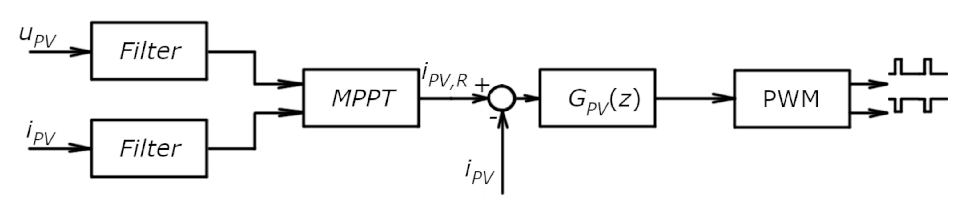
The control loop of the flyback DCDC converter is shown in Figure 4. In this figure, it can be seen that to control the panel’s current, the current controller changes the voltage on the PV panel. The voltage change is done by changing the duty cycle of the MOSFETs G f , 1 and G f , 2 .
The maximum power point tracking (MPPT) algorithm called “Incremental Conductance” [17] is employed to optimize the output of the PV panel, thus ensuring it operates at its peak power output. This algorithm dynamically adjusts the reference current i P V , R of the current controller G P V z while monitoring the voltage u P V of the PV panel. The panel’s power is easily calculated by knowing its voltage and current. Through iterative adjustments, the algorithm continuously refines the operating point of the panel until it identifies the maximum power point. This algorithm works like any other optimization algorithm. The function that is minimized, but in this case maximized, is the power of the PV panel. The optimization variable is only the panel’s voltage, because the panel’s current directly depends on the panel’s voltage, which simplifies the problem to a one-dimensional optimization task.
The MPPT algorithm uses the first-order condition for optimality:
P PV U PV , I PV U PV , 0 = 0 .
By arranging the above Equation (11), the equation which must be satisfied at the maximum power point of the PV panel can be derived, which is
dP dU = P I dI dU + P U dU dU = U dI dU + I = 0 .
Because this is a convex optimization problem, and the optimization function is 1D optimization, it only needs to be known where the PV panel’s working point is: left or right of its maximum power point. When the working power point of the PV panel is positioned either to the left or to the right of the maximum power point, the different equations will be satisfied. Specifically, if the working power point is to the left of the maximum power point, Equation
dP dU > 0 dI dU > I U ,
will be satisfied. On the other hand, if the working power point is to the right of the maximum power point, Equation
dP dU < 0 dI dU < I U .
will be satisfied. By knowing this, the algorithm can quickly know how to move the PV panel’s working point to reach its maximum power point.
The flyback converter’s current controller is achieved through the first-order transfer function
G PV z = 0.0917 z 0.07138 z 1 ,
which is implemented using the IIR filter structure. The controller has the feature of programmable output saturation. The current controller’s transfer function is inverted due to the decrease in current with a higher duty cycle of the flyback’s PWM. This is because the upper transistor is switched on longer than the lower one (Figure 3). The inverted function represents the PI controller with a gain of 0.07138 and an integral time constant of 7.026 × 10 5 s, thereby operating at a sample frequency of 50 kHz.
The MPPT algorithm has a sample time of 1 kHz because the solar temperature and irradiance of the PV panel have significant time dynamics constant. This algorithm changes the reference value of the current controller executed in the interrupt routine with a frequency of 50 kHz.
Two inverted PWM pulses are required to control the MOSFETs in Figure 3. The ePWM peripheral of the microcontroller generates a PWM signal frequency of 100 kHz because of the very small dynamics constant of the flyback DCDC converter. The hardware of the ePWM peripheral of the microcontroller ensures that the upper and lower MOSFETs are not turned on simultaneously. The dead-band generator submodule of the ePWM module assures this.
Because the degradation in the resolution of the duty cycle is increased by using the higher PWM frequency of the ePWM module, a high-resolution pulse width modulator (HRPWM) is used. It is used to increase the resolution of the PWM. This microcontroller’s microedge position step size (MEP) is typically around 150 ps, depending on the temperature and the microcontroller’s voltage. By using this submodule, the resolution of the PWM is increased by 7 bits for a PWM frequency of 100 kHz and the frequency of the microcontroller of 60 MHz.
To ensure safety, the ePWM peripheral is equipped with the Trip-Zone (TZ) submodule, along with the Digital Compare submodule and internal comparator of the microcontroller. These are set up to trigger a trip when the current from the PV panel reaches 10 A. However, due to current spikes at duty cycles under 1%, the Digital Compare submodule employs black window filtering to provide filtering.
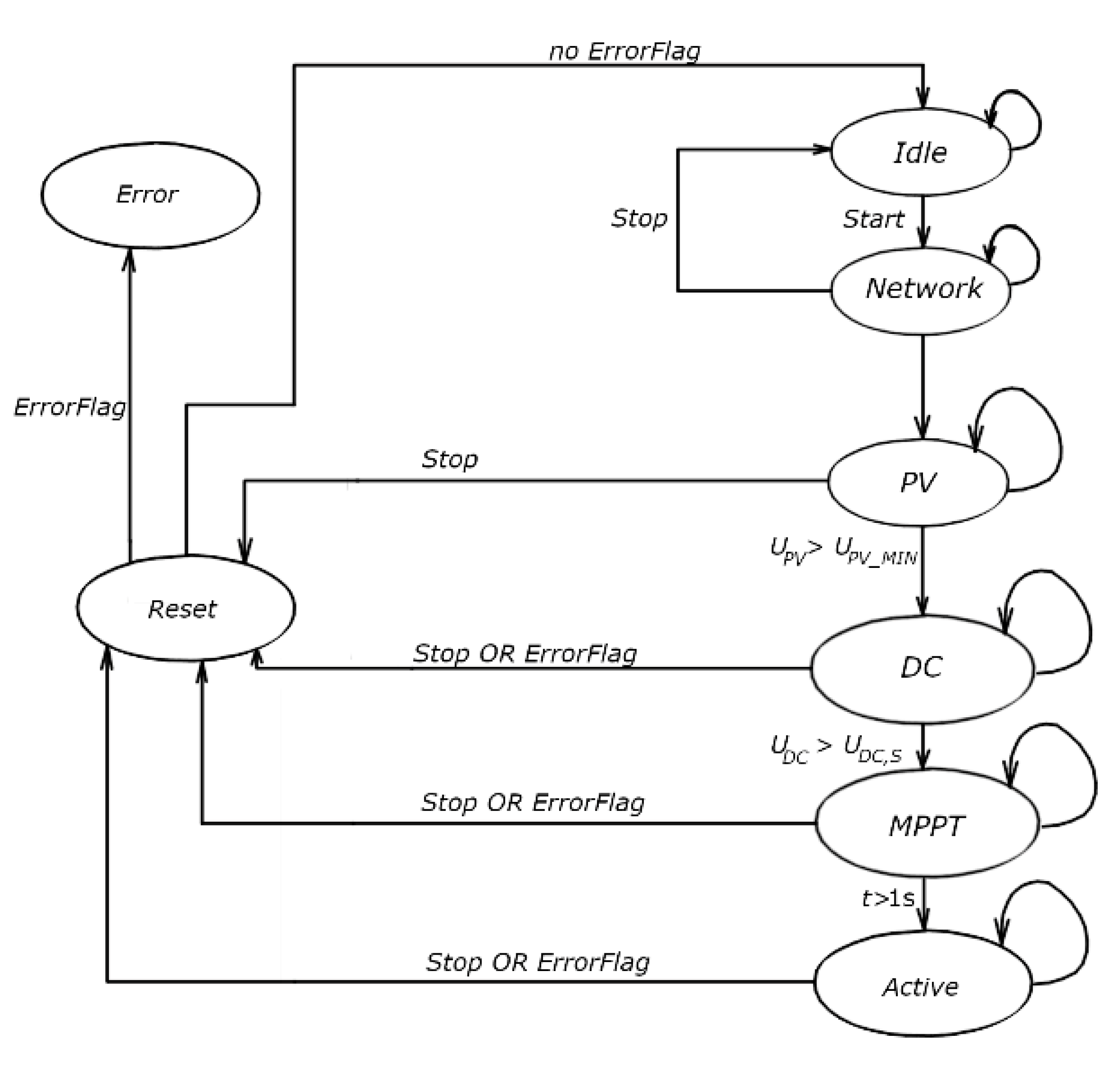
The flyback and inverter of the platform are closely integrated with the manufacturer’s advanced control algorithm. However, a separation between them is necessary for additional components to be connected to the platform’s DC bus. In addition, it is essential to modify the inverter to make it a grid-forming converter, thus enabling the energy to flow in both directions to and from the network. To achieve this, appropriate changes must be made to the state diagram of the platform shown in Figure 5.
The platform’s control algorithm includes a single state diagram, which is depicted in Figure 5. The “Idle” state represents the state where no energy conversion occurs. To activate the platform, the Start variable is used. The platform transitions from the “Idle” state to the “Network” state by setting this variable to a logical one.
The electric grid parameters are continuously monitored in a particular state of the platform. The state will persist until all the parameters are within the prescribed limits. The voltage and frequency of the electrical network are the parameters that are checked. From this platform state, it can be returned to the “Idle” state with the variable “Stop”. The network voltage must be in the range of 185 to 255 VRMS, while the frequency must be between −47 and 53 Hz to proceed to the next “PV” state.
In any of the states in the platform state diagram, the errors continuously checked are the network undervoltage, network overvoltage, the network underfrequency, and the network overfrequency. In contrast, the DC overvoltage and undervoltage are additionally checked in the states “DC”, “MPPT”, and “Active”.
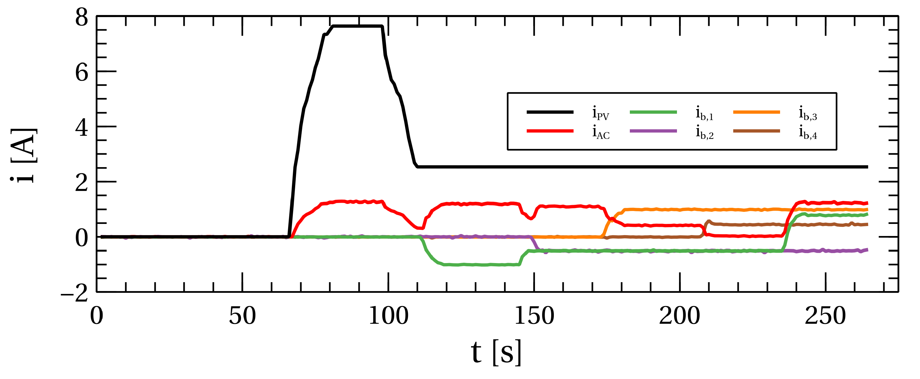
In the “PV” state, the PV panel voltage is checked. If this voltage is above 15 V, the current controller is activated, which maintains the current of a panel at 0.1 p.u. It controls the voltage at the panel clamps to achieve the desired constant panel current.
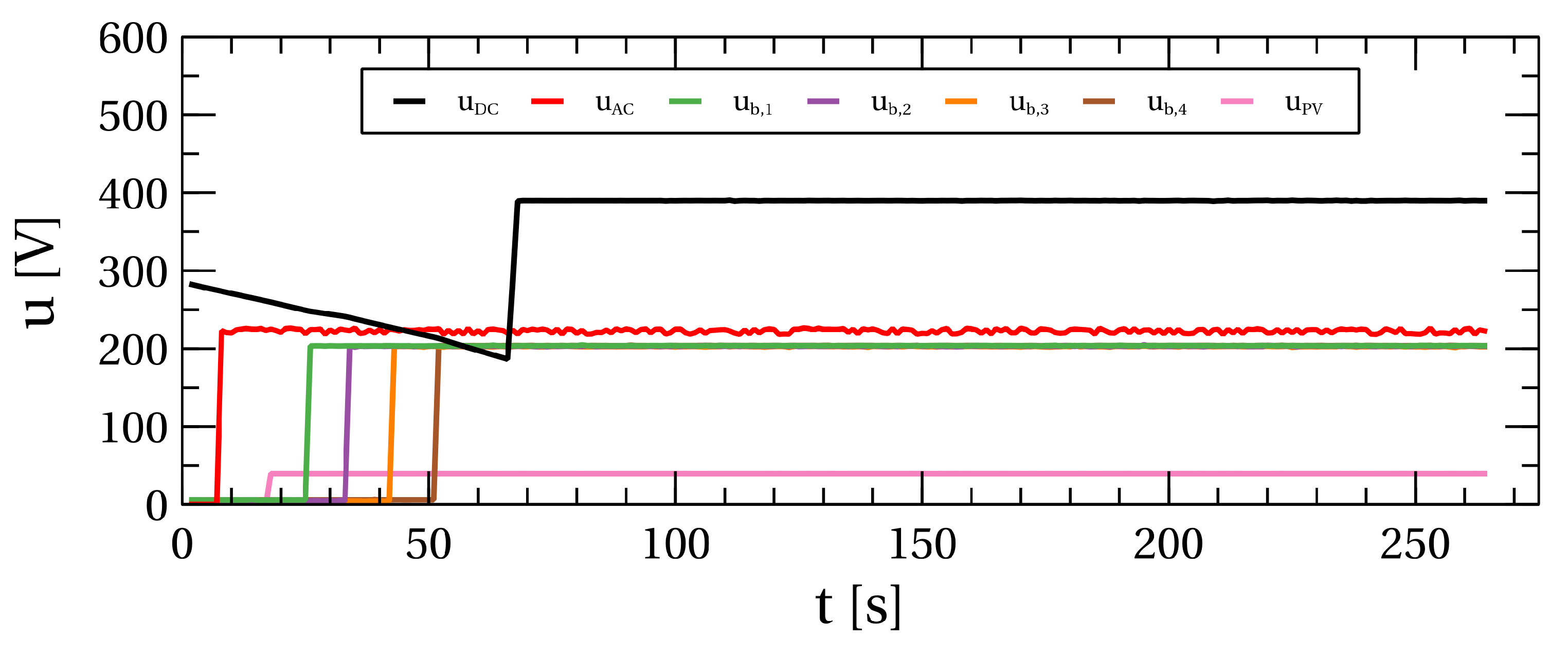
Now, the platform is in the “DC” state, where it waits for the voltage of the DC bus to rise to 386 V, which is defined with the constant variable U D C , S . As in the previous state, the network parameters are also continuously checked in this state. When the DC bus voltage rises over 386 V, the platform goes to the next state, the “MPPT” state, where the MPPT algorithm is activated. This state is used to delay transitioning to the next state, “Active”. This delay is introduced to make the lightweight transition from the current control of the PV panel to its maximum power control. The value of this delay is one second.
In the “Active” state, the current and voltage control of the inverter is activated. The cascade control system is used, where the current control of the network is the inner control loop, while the voltage control is the outer control loop. The current controller controls the amplitude of the current to the network, while the PLL maintains that the network current is in phase with the network voltage, which achieves the power factor of one. This current controller can be called the power controller because the network voltage has a constant amplitude value, which implies that the network power is proportional to the network current.
With the inner control loop, power to the network is controlled, while with the outer control loop, the reference to the power controller is defined by the voltage controller, i.e., the DC bus accumulated energy controller. This reference is defined depending on the accumulated energy in capacity. This controller maintains the constant energy in the DC bus by maintaining the DC bus voltage.
The “Reset” is used to reset the platform’s controllers, block pulses of the MOSFETS, and to check if any error occurred. The platform will go to the “Error” state for errors. In this state, the platform stays permanent; if there are no errors, the platform goes to the “Idle” state.
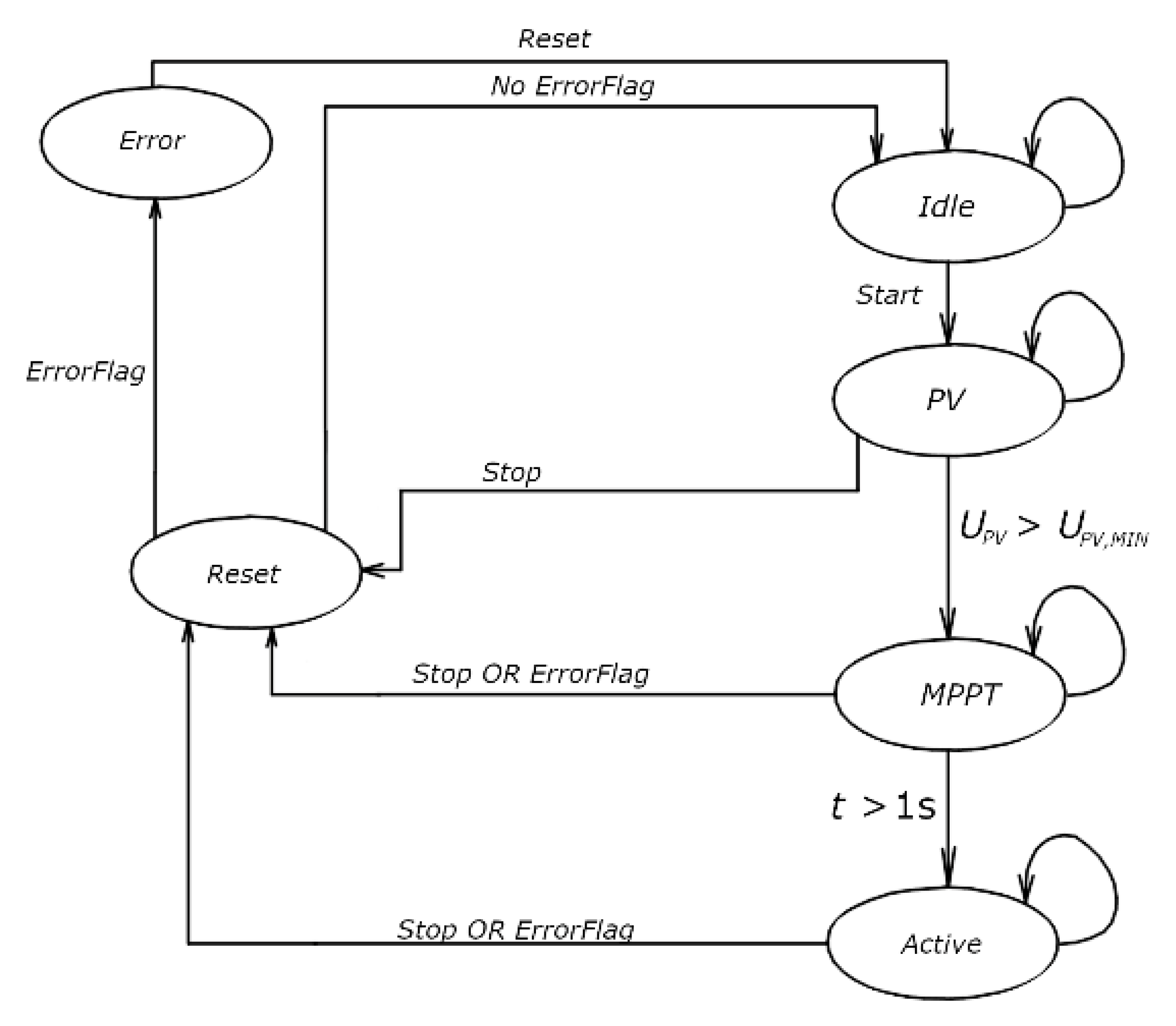
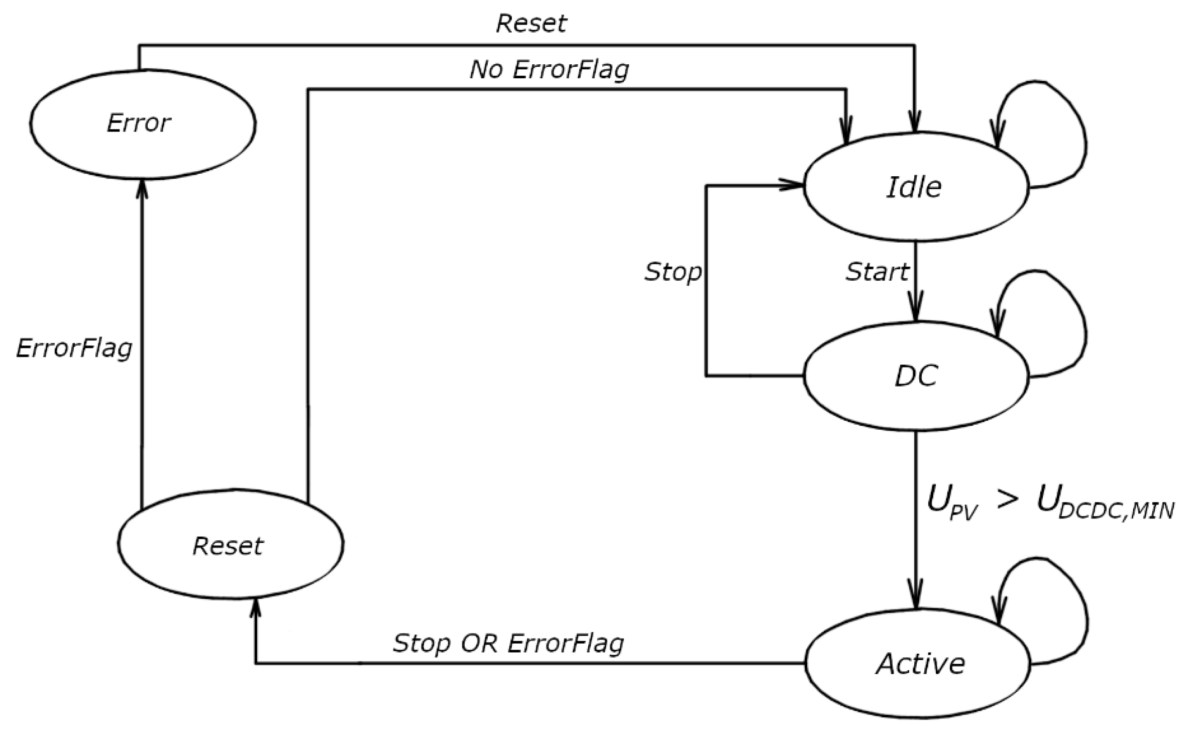
Two variables were introduced to store their states: “FlybackState”—used for the flyback converter—and “GridFormingState”—used for the grid-forming converter—to separate these two converters. The platform flyback converter’s modified supervisor control state diagram is shown on Figure 6. From the state diagram shown in Figure 6, it can be seen that it contains only states relevant to the flyback converter.
The flyback converter is in the “Idle” state in the nonactive state. It must go through two intermediate states from the “Idle” to the “Active” state. The first intermediate state is the “PV” state, where the voltage of the PV panel is checked. If the panel’s voltage is below the required minimum value U P V , M I N , it will stay in this state forever; if the PV voltage is above the minimum required, then it will go to the “MPPT” state, where the MPPT algorithm will be enabled if the variable EnableMPPT is in a logical one. The delay of one second is realized to achieve a smooth turn-on of this algorithm. After that, it will go to the “Active” state, where energy is converted between the PV panel and the DC bus.
From any of these states, the flyback converter goes to the “Reset” state by setting the variable “Stop” or if DC bus overvoltage occurs, which is around 405 V. From the “Reset” state, it goes to the “Idle” state if there were no errors. Otherwise, it goes to the “Error” state. To go from the “Error” state to the “Idle” state, the “ErrorFlag” needs to be reset by using the variable Reset of the flyback converter.
The error of the flyback converter can arise from bus overvoltage and/or overcurrent of the PV panel. The overcurrent can occur only in the “Active” state when the current controller and PWM are active. The “Reset” state is used to reset the controller and MPPT algorithm variables and to prepare the flyback converter for the following turn-on process.

3.2. Grid-Forming Converter

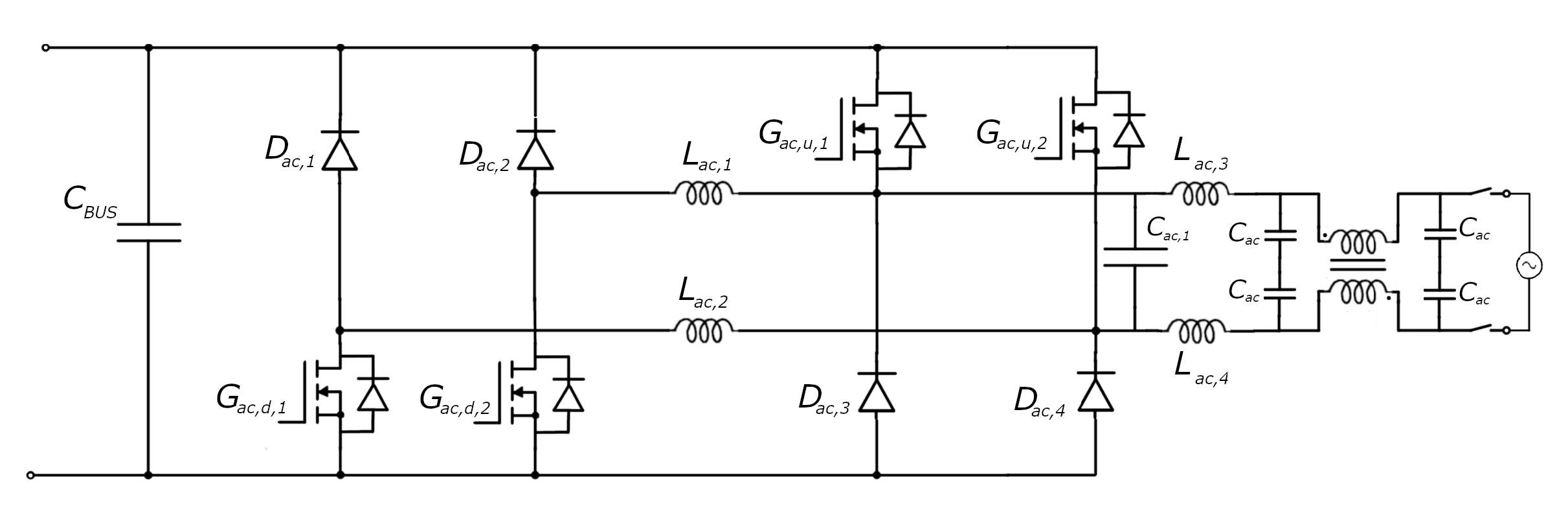
The grid-forming converter is used to connect the DC bus to the network. It consists of MOSFETs, which are used for its power switches. The voltage and current at the DCAC bridge’s output are shaped according to the grid’s needs to achieve the desired power flow. These waveforms are realized using the PWM modulation of the DC bus voltage. The lower harmonics at the grid-forming converter’s output are accomplished using a low-pass filter between the connection of the grid-forming converter’s bridge and the network.
Figure 7 shows the electric schematic of the DCAC platform’s converter, which has detailed parameters provided in Table 2. To achieve energy flow from the DC bus to the network, the voltage of the DC bus must be higher than the highest value of the network voltage. The converter is made of two step-down DCAC converters. They form sinusoids in the way that one is the positive part of the sinusoid, and the other is the negative part.
During the positive and negative values of the grid voltage, transistor pairs G a c , u , 1 G a c , d , 1 and G a c , u , 2 G a c , d , 2 are used, respectively. The PWM frequency of the nonsymmetric PWM of the MOSFETs of the converter used is 50 kHz. For generating this PWM, the ePWM 1 and ePWM 2 peripherals of the microcontroller are used.
The coils Lac,3, Lac,4 and the choke transformer suppress higher harmonics going to the grid and the noise caused by the parasitic capacitance between the ground and the supply line. The microcontroller controls a relay to disconnect the DCAC converter from the network physically.
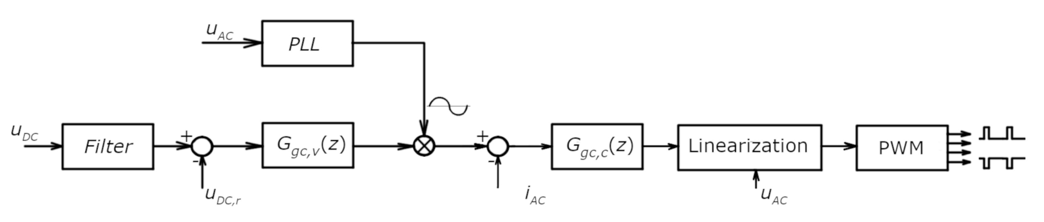
The converter control algorithm generates current toward the network to regulate the voltage of the DC bus. Since the network voltage is fixed and determined by the network, the current serves as the means for the control algorithm to adjust the output power. This enables the microgrid to achieve a stationary power flow.
The control is realized by nested loops, shown in Figure 8, where the inner control loop is the current control, while the upper control loop is the voltage control of the DC bus. The current controller G g c , c z changes the PWM duty cycle to ensure that the current of the grid-forming converter follows its reference value. A phase lock loop (PLL) system [18] generates the current controller’s reference value, which is in phase with the network voltage, thereby assuring that the power factor one has a sine shape. To regulate the power flow, the voltage controller G g c , v z changes the amplitude of the current reference, which is achieved by the multiplication operation between the PLL and the voltage controller output.
Minor hardware modification is needed to use the same energy circuit of the platform’s inverter to become the grid-forming converter. It involves bridging two inductors, L a c , 1 and L a c , 2 , with copper wires, as shown in Figure 7. With this modification, the energy circuit now looks like the standard H bridge.
This modification also demands a change in the PWM and the platform’s linearization algorithm, as shown in Figure 8. The standard PWM signals of this bridge are realized using the ePWM modules of the DSP. By changing the duty cycle d g c of this PWM, the voltage’s average value u ¯ g c at the output of this bridge is changed, and it can be changed from the minus to plus value of the DC bus voltage.
The voltage waveform generated at the grid-forming converter’s output is
u gc t = u DC t d gc T u DC d gc T < t T .
The average value of this waveform for the PWM period is
u ¯ gc d = 1 T 0 T u gc dt = 2 d gc 1 u dc .
The current controller gives the value of the voltage drop on the filter Δ g c , from which the linearization block in Figure 8 needs to calculate the duty cycle ( d g c ) that will produce it. This voltage drop is calculated using the following equation:
Δ gc kT = u gc d gc kT u AC = 2 d gc kT 1 u DC + u AC .
This voltage drop can only be changed in discreet times 2kTPWM. The equation used for this linearization block, shown in Figure 8 for the standard H bridge and its PWM and given after arrangement (18), is
d g c = Δ gc + u AC + u DC 2 u DC .
With this hardware and software modification, bidirectional energy flow becomes achievable. The voltage controller’s lower output signal saturation can now be set from 0 p.u. to −0.95 p.u. The current controller is realized using the transfer function
G gc z = b 3 z 3 + b 2 z 2 + b 1 z 1 + b 0 a 3 z 3 + a 2 z 2 + a 1 z 1 + 1 ,
which achieves a bandwidth of 1.2 kHz and a gain of more than 20 dB for frequencies up to 200 Hz and the following parameters: b0 = 0.29, b 1 = −0.32, b 3 = −0.262, a 1 = 1.584, a 2 = −0.698, and a 3 = 0.114.
The current dynamics of the grid-forming converter are described by Equation
i A C s = Δ gc ( s ) z gc ( s ) ,
where z g c takes into account the network impedance and the grid-forming converter filter. This impedance of the platform is
z gc = z AC z f + z i ( z AC + z f ) z AC + z f ,
where zAC is the network impedance, zf is the filter impedance, and zi is the grid-forming converter impedance.
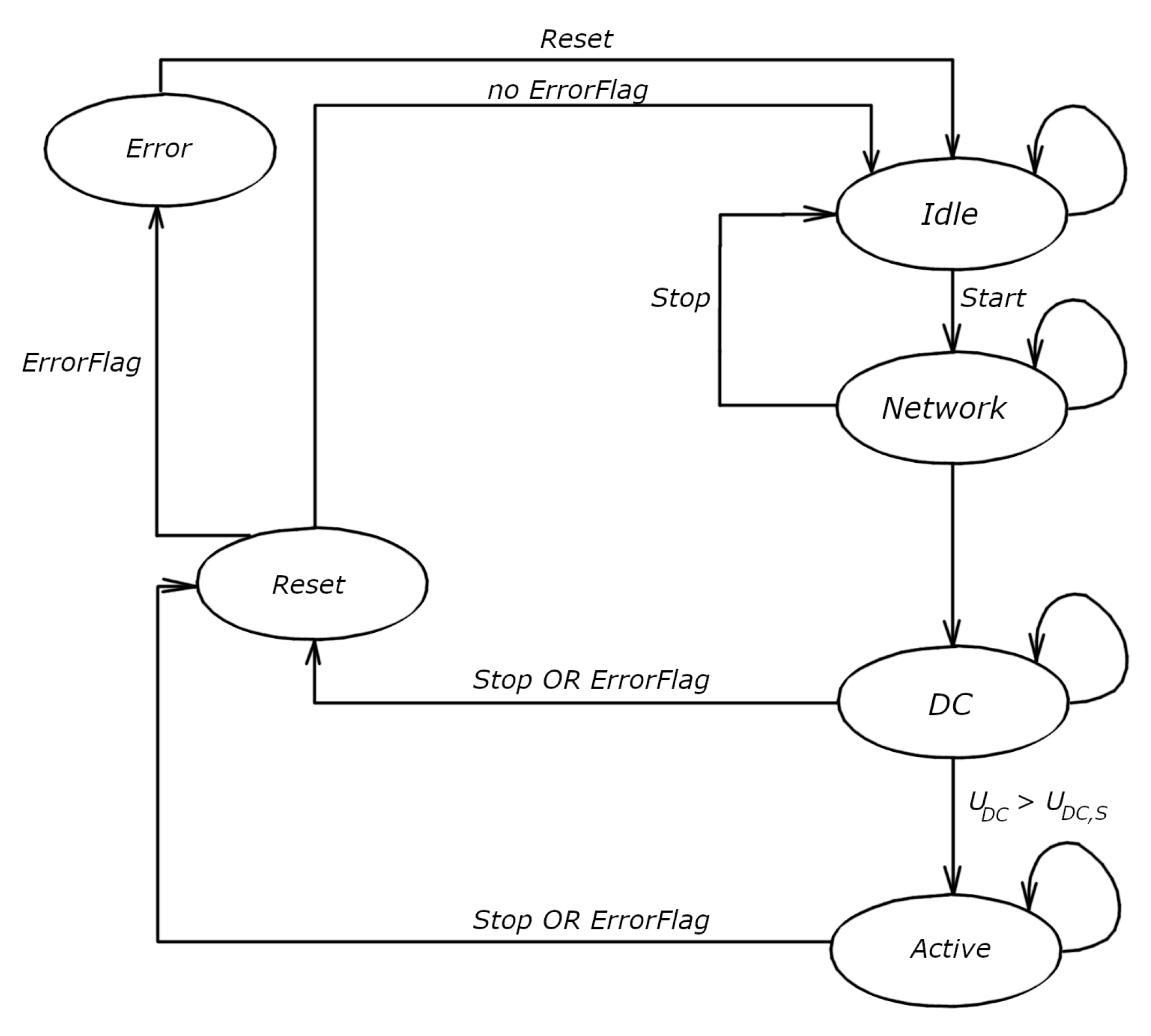
The modified state diagram of the grid-forming converter is shown in Figure 9. States “PV” and “MPPT” are no longer in the state diagram of the grid-forming converter because these states are closely associated with the flyback converter. From the “Idle” state, where the gird forming converter is nonactive, it goes to the “Active” state through two intermediate states. These states are “Network” and “DC”. When the grid-forming converter is inactive, it is in the “Idle” state shown in Figure 9. By setting variable Start, the grid-forming converter goes to the “Network” state, where the network parameters are checked. This state will stay until the network parameters are within limits. If these parameters are within limits, the grid-forming converter will go to the next state, the “DC” state. In this state, the DC voltage value is continuously checked. The grid-forming converter goes to the “Active” state when its value exceeds the minimum start voltage U D C , S . In this state, the transfer of energy from the DC bus to the network and vice versa is achieved, i.e., a two-way transfer of energy.
The grid-forming converter goes through the “Reset” state using the Stop variable, where all states of the controllers are reset and initialized. If this variable causes the grid-forming converter to go to the “Reset” state, then it will automatically go to the “Idle” state; otherwise, if the “ErrorFlag” caused this, then it will go to the “Error” state and stay in it. To go to the “Idle” state, the user must reset the error by setting this flag to one. The network overcurrent, the network overvoltage, the network undervoltage, the network overfrequency, the network underfrequency, and the DC bus undervoltage can set this flag.

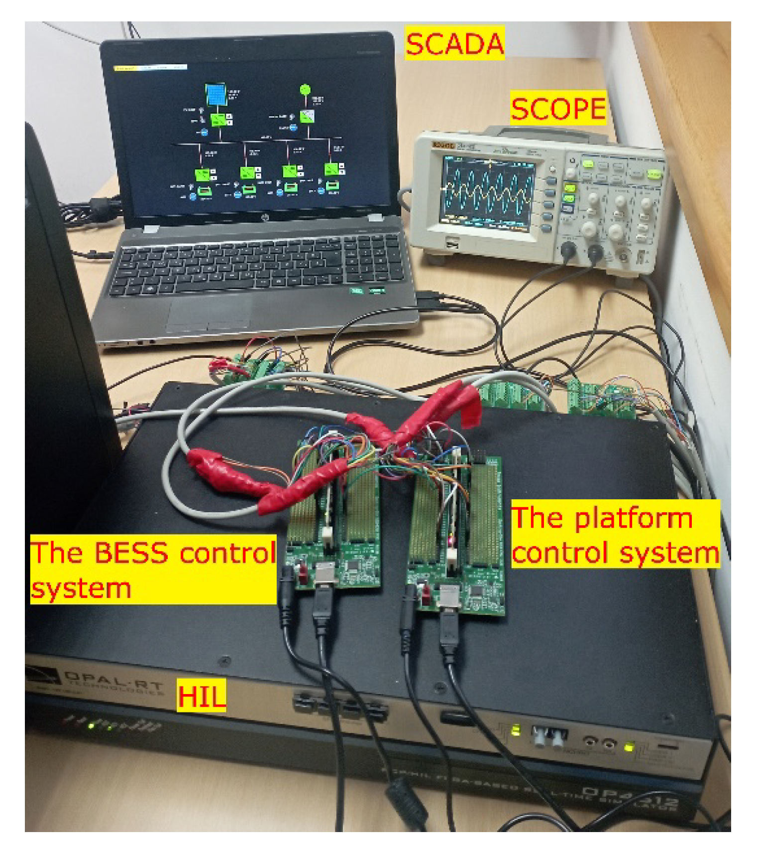
3.3. DCDC Converters and BESS

The DCDC battery converter shown in Figure 10 manages the charging and discharging of the i-th battery. Its parameters are shown in Table 3. It establishes the connection between the battery pack and the DC bus. The energy circuit of the DCDC battery converter comprises a buck DC converter combined with a boost DC converter (the DCDC buck–boost converter). The buck DC converter controls the flow of electrical energy from the DC bus to the batteries, thus regulating the charging current. Conversely, the boost DC converter regulates the battery discharge current. Figure 10 illustrates that the buck DC converter is implemented using the upper MOSFET transistor and the lower MOSFET diode.
In contrast, the boost DC converter utilizes the lower MOSFET transistor and the upper MOSFET diode. The control algorithm is executed within a microprocessor that generates control signals based on sensor inputs (the voltage and current measuring). These control signals are then sent to the transistors to control the system behavior.
An inductor is connected in series with the battery pack to mitigate the current ripple caused by pulse width modulation (PWM) regulation and reduce the stress on the microprocessor generating the PWM signal. A higher inductance allows for a lower switching frequency of the transistors, thereby achieving the same result and enabling the use of a less powerful (less expensive) microprocessor. This type of DCDC converter can operate in the first and fourth quadrants, meaning that the voltage polarity remains constant (the DC bus voltage must always be higher than the battery pack voltage; otherwise, the converter is turned off), while the current can flow in both directions (charging and discharging the batteries). The supervisory algorithm continuously measures the voltage of the DC bus and the battery stack to ensure a constant voltage polarity. An appropriate relay exclusively connects these two energy circuits under the corresponding conditions (when the DC bus voltage is higher than the battery pack voltage; otherwise, the batteries are physically disconnected).
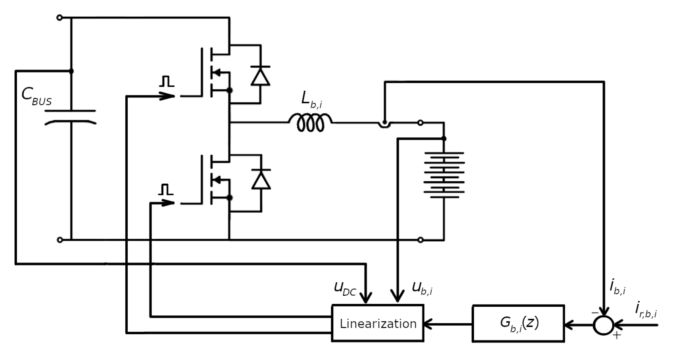
The current control loop of the DCDC buck–boost converter is depicted in Figure 10. This control loop comprises a single control loop that incorporates a current regulator G b , i ( z ) (PI controller realized with CNTL_PI_IQ algorithm of Texas Instruments library) responsible for maintaining the desired reference value for the batteries’ charging or discharging current, depending on the specified polarity.
In addition to the current controller, the control loop includes a linearization element that addresses the nonlinear dynamics associated with the battery charging or discharging process. Consequently, measuring the voltages of the DC bus and the connected battery pack, together with the battery stack’s current, is necessary.
The linearization is made in the way that the controller is controlling the voltage drop across the inductor Lb,i, as shown in Figure 10. To obtain linear characteristics in the control loop, first, it is needed to obtain a relation regarding how the average voltage on the inductor u ¯ d c d c , i depends according to the duty cycle ddcdc,i of the PWM, which is generated by the ePWM module of the microcontroller F28035. It is necessary to emphasize that the PWM dead time is not considered. The voltage waveform generated at the DCDC converter’s output is
u dcdc , i t = u DC u b , i t d dcdc , i T u b , i d dcdc , i T < t T .
The generated waveform average value on the inductance L b , i for the PWM period of the DCDC converter is
u ¯ dcdc , i d = 1 T 0 T u dcdc , i dt = u dc d dcdc , i u b , i .
The linearization block of the current control, shown in Figure 3, is realized by Equation (24). Its output represents the average voltage on the inductance L b , i . The dynamics of the current are described by the following equation:
i b , i s = 1 L b , i s u dcdc , i ( s ) .
The controller’s limits need to be adjusted so that there is no problem with the wind-up effect, which, without this adjustment, will arise. To calculate these limits of the controller, first, it is necessary to define the area in which the physical values of the DC voltage u D C , duty cycle d d c d c , i , and battery u b , i will be. These are
U min , DC u DC U max , DC ,
U min , b u b , i U max , b ,
and
0 d dcdc , i 1 .
These upper nonequations need to be satisfied all the time. The limits for the average voltage drop are given, thus ensuring that a wind-up effect will not arise and solving these nonequations. The limit values of the current controller G b , i z are
U ¯ min = U min , b ,
for the lower voltage drop, while
U ¯ max = U min , DC U max , b ,
defines the upper voltage drop.
Each battery block connected to the system has its dedicated current regulator responsible for maintaining the charge and discharge current. A superior algorithm governs this regulator, thereby determining the operating state of the converter based on the present electrical quantities and user commands. Additionally, the algorithm establishes the permissible operating conditions for the regulator, considering the voltages of the DC bus and batteries, and implements protective functions that trigger a transition to the “Error” state in the event of irregularities. When the converter is turned off, it is in the “Idle” state, while during battery charging or discharging, it operates in the “Active” state. The operation of the superior algorithm, represented by the DCDC battery converter, is described using a state diagram depicted in Figure 11.
In the “Idle” state, the power circuit of the DCDC battery converter is isolated from the DC bus using a relay, the current regulator is deactivated, and impulses to the MOSFET transistors are blocked. Setting the variable Start of the DCDC converter to a logical one transitions the battery DCDC converter to the “DC” state, where it verifies the voltage of the DC bus. The current DC bus voltage is compared with predetermined values. The algorithm ensures that the relay connecting the battery DCDC converters to the DC bus is activated when the DC bus voltage exceeds 20% over the maximum voltage value of the batteries connected in the serial with a 100% SOC (state of charge). From the “DC” state, it is possible to return to the “Idle” state by setting the variable Stop of the DCDC converter to a logical one. If the conditions for correct operation are met, the “DC” state transitions to the “Active” state. In the “Active” state, the current regulator is active, thus maintaining the specified charging or discharging current for the batteries. The DC bus and battery voltages are continuously monitored, thereby ensuring that they remain within permissible limits. The converter enters the “Reset” state if any value exceeds the permissible limits. In this state, the battery current regulator is deactivated (transistor impulses are blocked, thus preventing conduction), and the relay connecting the DC bus and the DCDC battery converter is disconnected, thereby physically separating the energy circuits. Subsequently, from the “Reset1,2” state, after blocking the transistors and disconnecting the relay, the converter automatically transitions to the “Error” state. Manual error checking and resetting are required to reactivate the converter. Setting the variable Reset confirms that the error has been resolved, thus allowing the DCDC converter to return to the “Idle” state.

3.4. SCADA of the Microgrid

To control the elements of the microgrid, the SCADA system is realized in the JAVA programming language. The connections to the DSPs of the platform and BESSs are realized by using the JTAG communication of the DSPs, which is also used for downloading the algorithm to the FLASH memory and debugging in the real-time mode of operation. Using the Code Composer Studio v12.1.0 debug server, SCADA is made as a client that connects using the TCP/IP.
To control the elements of the platform and DCDC converter of the BESS, the created GUI is part of the data acquisition system (SCADA). The main page of the SCADA system is shown in Figure 12. There are four options, which are located in the upper left corner. These options are “Puni zaslon” for maximizing the SCADA system to full screen or back in the window mode; “Sustav”, which shows the schema of the microgrid and elements like buttons and switches to control the microgrid’s elements; “Logovi”, which shows the state change and the errors to see the reason of the state change of the elements, and “Grafovi”, which shows the waveforms of the measured signals of the microgrid.
The measured values from the sensors of the platform and BESS are shown next to their symbols at the option “Sustav”. The measured values are the voltages, currents, and power of the converters, as well as the PV panel, the grid, and the batteries. These values can be recorded in a CSV file using the “Snimanje” option, which is placed in the “Grafovi” option. This option is used for testing in the next chapter of this paper.

4. Experimental Setup

The experimental setup made in the Faculty of Electrical Engineering, Mechanical Engineering and Naval Architecture is shown in Figure 13 and Figure 14. The hardware used for the hardware-in-the-loop (HIL) was the OP4512 of the manufacturer OPAL-RT, Montréal, QC, Canada; its properties are given in Table 4. The microgrid model, shown in Figure 1, was implemented into the FPGA of the real-time hardware. The FPGA was used because of the high PWM frequency of the flyback converter, which is 100 kHz. The FPGA was used to simulate the flyback converter, the grid-forming converter, four DCDC converters of the batteries, and electric circuits to detect errors.
The control algorithm of the PV panel and the grid-forming converter was implemented in the first DSP of Texas Instruments, Dallas, TX, USA TMS320F28035 of the platform, while the control algorithm of the four DCDC converters of the batteries was implemented in the second DSP with the same designation, which are shown in Figure 13. For these two DSPs, the docking station TMDSDOCK28035 was used for JTAG debugging and a straightforward approach to the digital and analogue signals. JTAG communication was used to program, debug, and connect the SCADA program with these DSPs. Using this JTAG, the SCADA program can read and write appropriate locations in memories of the DPSs and, with this, can change the reference values of the controllers, turn on or off converters, and read values like the currents, powers, and voltages.
The appropriate steps have been taken to test the microgrid and its control algorithms in normal operating mode, as described in the following subchapters. It was tested in various hazard scenarios, wherein its control algorithm needed to prevent showing the behavior of the microgrid in error situations. These scenarios are the overcurrent of the converters, the overvoltage of the DC bus, the undervoltage of the batteries, the frequency shift, and others.

4.1. The Microgrid Operation

Various situations were made to test the microgrid operation by turning on or off the converters and changing their reference values. Different microgrid operation modes were realized through these changes, such as B2B, P2B, P2G, G2B, B2G, and the combinations of these modes. Reference directions of the energy flow in the microgrid are shown in Figure 2.
In the first step, the AC voltage of the grid u A C was connected to the virtual connections of the platform, as shown in Figure 15. The network voltage was measured at approximately 220 V and was brought to the platform at 8 s. Once the voltage was turned on, the virtual PV panel u P V and batteries were connected to their respective DCDC converters, starting from battery one u b , 1 to battery four u b , 4 . All batteries had a voltage of approximately 200 V.
The grid-forming converter was turned on the moment after the flyback converter of the PV panel at 60 s. The reference value of the current controller was set to 7.6 A at 66 s to see the reaction of the other elements of the microgrid to a significant increase in the power production p P V of the PV panel. The grid-forming converter was in the “Idle” state. It was waiting for the voltage of the DC bus u D C to increase over U D C , S voltage, which was set in the control algorithm of the grid-forming converter at 386 V. When the DC bus voltage was increased over that value, which was at 68 s, the grid-forming converter state was changed to the “Active” state. In this state, its current and voltage controllers are active, and to maintain the energy, i.e., the DC bus voltage, the current in phase i A C with the grid voltage was injected into the grid (Figure 16). The stationary state was reached when the energy flow from the PV panel became equal to the active energy flow to the grid. This can be seen in Figure 17 at 90 s. In this stationary state, the efficiency of the DCDC converter of the PV panel and the grid-forming converter was around 93%, which is the platform’s efficiency. The microgrid had one mode of operation, and that was the PV2G.
At 100 s, the reference value of the current controller of the PV panel was decreased to 2.5 A, and after that, the reference value of the current controller of the battery one was reduced to −1 A. With this, battery one was discharging with a continuous current of 1 A and a power p b , 1 of 205 W. The voltage controller of the DC bus of the grid-forming converter gave the order to increase the power to the electric grid p A C from the DC bus to maintain the voltage of the DC bus. From Figure 15, it can be seen that the voltage of the DC bus was constant because of the fast reaction of this controller. The efficiency of the microgrid was 87% according to Figure 17. In this situation, the microgrid operated in two modes, which were 67% B2G and 33% P2G.
The reference of the current controller of battery two was decreased to −0.5A, while the current controller reference value of battery one was increased to −0.5A. With this change, there should not be a change in the power, but because the microgrid has smaller effectivity (81%) at this working point, the power to the grid was lower from the previous working point for 20W. In this working point, there were B2G and P2G operating modes.
The following working point was achieved by turning on the DCDC converter of battery three and setting the current controller reference to 1 A. In this case, there were two working modes: P2G and B2B. The share of individual modes was 33% for P2G and 67% for B2B. The efficiency of this working point was 97%. The waveform of the grid current and voltage shown in Figure 18 was measured by the oscilloscope connected to the analogue outputs of the HIL.
The DCDC converter of battery four was turned on, and its reference value was set to 0.5 A at 208 s. With this, the energy to the grid was reduced near 0 W, and now there was no P2G operation mode, only the B2B and P2B operating modes.
Battery one was switched from the discharging to the charging mode to 0.8 A at 234 s. To compensate for the lack of energy flow to the DC bus and to maintain the voltage of the DC bus, the voltage controller changed the direction of the power flow. This was achieved by inverting the injected current to the grid, as shown in Figure 19. As seen in Figure 15, the DC bus voltage remained steady. The microgrid operated with an efficiency of 96% in three modes: B2B, G2B and P2B, with a distribution of 21%, 58%, and 21%, respectively.

4.2. The Microgrid Error Operation

The control algorithm of the PV panel can detect two types of errors—the overcurrent and overvoltage of the DC bus. If any of these errors are detected, the PV panel will enter the error state. However, the PV panel can be reset to the “Idle” state by pressing the “Reset” button in the SCADA program.
The grid-forming converter constantly checks for overcurrent from the network side. If such an event occurs, the PWM pulses will be disconnected using the trip subsystem of the DSP. The relay with the corresponding GPIO DSP pin will physically disconnect the microgrid from the network. During operation, the control algorithm of the grid-forming converter monitors the network frequency and voltage. If these values fall outside the permitted range, the grid-forming converter will go into the error state.
The BESS comprises four DCDC converters with batteries, and it also has overcurrent protection. The DC bus voltage is continuously monitored, and if it exceeds the defined overvoltage value, the control algorithm will turn off the pulses of the DCDC converters and physically disconnect the converters from the DC bus using a relay. If the DC bus voltage falls below the undervoltage value, the converter will also be disconnected from the DC bus.
The microgrid was purposely brought to these error situations by turning on or off the converters and changing their reference values in the way that these errors are produced. In Figure 20, the time at which the AC voltage of the grid was brought to the platform, together with the connection of the BESS batteries, can be seen. The AC voltage was 220 VRMS, while the voltages of the batteries were around 200 V.
After bringing the voltages of the AC network and the batteries, the grid-forming converter was turned on, and because the network voltage and frequency were within limits, it went to the state “MonitorDCBus”. In this state, it continuously checks the voltage of the DC bus. The flyback converter of the PV panel was turned on, and its current reference value was set to 7.19 A, thus resulting in a power of 280 W.
At 50 s, the reference value of the PV panel was continuously increased, which produced the overcurrent of the grid-forming converter, which can be seen in Figure 21, which gave the grid-forming converter power of 10% over its nominal power. The first fallen element in this error situation was the grid-forming converter because of its overcurrent protection (Figure 9). Now, because there was no power flow of the excess energy to the network, the voltage of the DC bus was continuously increasing, as shown in Figure 20. When the voltage of the DC bus increased over 4% over the nominal working voltage of the DC bus at which the reference value of the voltage controller of the grid-forming converter was set, the flyback converter went to an error overvoltage state (Figure 6). With this, the DC bus’s overvoltage protection and the grid-forming converter’s overcurrent protection were achieved.
At 60 s, the grid-forming converter was turned on. Because the voltage of the DC bus was over the value U D C , S , the grid-forming converter went to the “Active” state (Figure 9). Shortly after, the flyback converter was turned on, and its current reference value was set to 4 A, which gave the PV panel power of 160 W. The DCDC converter of battery four was connected at 74 s, and its reference current value was set to −0.3 A, which produced the battery two discharging power of 60 W. This increased energy flow would produce an increase in the DC bus voltage, which the control algorithm of the grid-forming converter prevented by increasing the energy flow to the network to 188 W. From Figure 20, it can be seen that there was no voltage rise, or what would be if the grid-forming converter control system did not react in time. At 86 s, the current value of the DCDC converter of battery four was continuously decreased until the overcurrent protection of the grid-forming converter was activated. The grid-forming converter went to the error state and disconnected the microgrid from the network. The PV panel and the DCDC converter of battery four still gave the energy to the DC bus, which caused an increase in the voltage of the DC bus, which can be seen in Figure 20. When this voltage had gone over 4% of the nominal DC bus voltage, it triggered the overvoltage protection of the flyback converter and the DCDC converter of battery four. They went to their error states (Figure 6 and Figure 11). With this, the overvoltage protection of the BESS and the flyback converter and their reaction to the grid-forming converter outage were tested.
The grid-forming converter was turned on, together with the DCDC converter of battery one, to test the overcurrent protection of the grid-forming converter when the energy flow is from the network to the DC bus at 100 s. The reference value of the DCDC battery two was set to 1 A, which gave the battery one a charging power of 200 W. Because the voltage transfer ratio was near one, the RMS current value of the grid-forming converter was approximately equal to the charging current of battery one, as seen in Figure 21. The power of the grid-forming converter was negative, which means that the energy was transferred from the network to the DC bus. In contrast, the positive value of the DCDC converter battery one power means that the energy was transferred from the capacities in the DC bus to the battery one. The reference value of the DCDC converter one at 120 s was continuously increased until the overcurrent protection of the grid-forming converter was activated. This current protection limited the power of the grid-forming converter to 300 W, which is shown in Figure 22 for positive and negative energy flow. This means that the control algorithm will ensure that the power will never go 7% over the nominal power value. Because the grid-forming converter dropped out first, there was no energy flow to the DC bus; only the energy flowed out of it. This introduced a decrease in the voltage of the DC bus, which is shown in Figure 20 at 120 s. When the voltage dropped below 250 V, the DCDC converter went to an error state, its PWM impulses were blocked, and it was physically disconnected from the DC bus using the relay. This is the undervoltage protection that the flyback converter does not have in its state diagram.
At 132 s, the flyback converter was turned on, together with the grid-forming converter. The grid-forming converter was in the “DC” state as long the DC bus voltage was below U D C , S , which was set to 386 V. At the same time, the flyback converter was in an “Active” state. The flyback reference current value was continuously increased to 2.23 A. The energy from the PV panel was first used to increase the voltage of the DC bus. When this voltage exceeded U D C , S , the grid-forming converter was synchronized and connected to the network using the relay. After connecting the grid-forming converter to the network, the DCDC converter of the battery one was turned on. Because the DC bus voltage was within the operation limits, the DCDC converter went from the “DC” state to the “Active” state. Its charging power was set to 213 W. To maintain the DC bus voltage, the grid-forming converter needed to bring the energy from the network, which can be seen in Figure 22. The power of the grid-forming converter had a negative value. To see the impact of other microgrid elements, at 147 s and 156 s, the DCDC converters of batteries two and three were turned on, respectively. The discharging power of the DCDC converter of battery two was set to 98 W, while the charging power of the DCDC converter of battery three was set to 111 W. To maintain the DC bus voltage, the grid-forming converter needed to bring the energy from the network with an energy rate of 149 W. Using the OPAL-RT terminal, the network’s voltage was decreased to 200 V at 173 s. The grid-forming converter detected this, and because of this, it went to the error state. Because the stationary state was disrupted, the voltage of the DC bus started to decrease. When this voltage decreased below U D C D C , M I N , the DCDC converters of batteries one, two, and three went to the error state and were disconnected from the DC bus. Now, the only element connected to the DC bus was the flyback converter, which continuously brought the energy to the DC bus. This caused an increase in the DC bus’s voltage until it exceeded 4% of the nominal DC bus voltage, which triggered the overvoltage protection of the flyback converter. All microgrid elements were now in the error states except the DCDC converter of battery four. With these, the error situations that can arise in the microgrid operation were tested, and it can be seen that the microgrid was within the allowed limits.

5. Conclusions

This paper proposed and described the modification of the platform of the manufacturer Texas Instruments and how to incorporate it in the microgrid, which has a single bus topology with a unipolar configuration and a BESS system with four battery packs. This modification of the platform code separates the flyback converter’s algorithm from the inverter’s algorithm. The platform’s inverter with hardware modification was made to become the standard H bridge and to work like the grid-forming converter. This made two-way energy transfer possible with this platform.
The algorithm of the BESS system was made from scratch and adapted to work with the flyback converter and the grid-forming converter. The coordination was made using the physical values of the microgrid and the supervisory control, which were described using the state diagrams in the paper.
With all of these, the microgrid elements work together, and they realize different modes of operation in microgrids like B2B, B2G, P2B, P2G, and G2B. All these modes of operation were tested in real-time simulation with the HIL of the OPAL-RT. The results, where different operation modes and combinations were made, have been described and analyzed. Through testing of the microgrid and its control algorithm, it was determined that its efficiency depends on its working point, i.e., on the share of the microgrid’s operating modes. The achieved efficiency of the microgrid with the mentioned modification resulted in about 91%.
A separate HIL simulation was made to test the error situations which can arise in the operation of the microgrid. The microgrid’s physical values were returned in standard working intervals from all tested error situations, and the microgrid was safely turned off.

Author Contributions

Conceptualization, D.J. (Danijel Jolevski) and D.J. (Damir Jakus); Methodology, D.J. (Danijel Jolevski); Software, D.J. (Danijel Jolevski); Validation, J.V.; Formal analysis, D.J. (Danijel Jolevski); Investigation, J.N.; Resources, D.J. (Damir Jakus); Data curation, J.V.; Writing – original draft, D.J. (Danijel Jolevski) and D.J. (Damir Jakus); Visualization, D.J. (Danijel Jolevski) and J.N.; Project administration, D.J. (Damir Jakus); Funding acquisition, D.J. (Damir Jakus). All authors have read and agreed to the published version of the manuscript.

Funding

This work was funded by the European Union through the European Regional Development Fund Operational Programme Competitiveness and Cohesion 2014–2020 of the Republic of Croatia under project KK.01.2.1.02.0228: “Research and development of smart-grid charging station for electric vehicles within the construction of a rotary parking system”.

Data Availability Statement

The original contributions presented in the study are included in the article, further inquiries can be directed to the corresponding author.

Conflicts of Interest

The authors declare no conflict of interest.

References

  1. Braun, M.; Stetz, T.; Bründlinger, R.; Mayr, C.; Ogimoto, K.; Hatta, H.; Kobayashi, H.; Kroposki, B.; Mather, B.; Coddington, M.; et al. Is the distribution grid ready to accept large-scale photovoltaic deployment? State of the art, progress, and future prospects. Prog. Photovoltaics Res. Appl. 2012, 20, 681–697. [Google Scholar] [CrossRef]
  2. Zubieta, L.E. Are Microgrids the Future of Energy?: DC Microgrids from Concept to Demonstration to Deployment. IEEE Electrif. Mag. 2016, 4, 37–44. [Google Scholar] [CrossRef]
  3. Shahid, M.U.; Khan, M.M.; Hashmi, K.; Habib, S.; Jiang, H.; Tang, H. A Control Methodology for Load Sharing System Restoration in Islanded DC Micro Grid with Faulty Communication Links. Electronics 2018, 7, 90. [Google Scholar] [CrossRef]
  4. Thounthong, P.; Mungporn, P.; Pierfederici, S.; Guilbert, D.; Bizon, N. Adaptive Control of Fuel Cell Converter Based on a New Hamiltonian Energy Function for Stabilizing the DC Bus in DC Microgrid Applications. Mathematics 2020, 8, 2035. [Google Scholar] [CrossRef]
  5. Pires, V.F.; Cordeiro, A.; Roncero-Clemente, C.; Rivera, S.; Dragičević, T. DC–DC Converters for Bipolar Microgrid Voltage Balancing: A Comprehensive Review of Architectures and Topologies. IEEE J. Emerg. Sel. Top. Power Electron. 2023, 11, 981–998. [Google Scholar] [CrossRef]
  6. Prabhakaran, P.; Agarwal, V. Novel Four-Port DC–DC Converter for Interfacing Solar PV–Fuel Cell Hybrid Sources with Low-Voltage Bipolar DC Microgrids. IEEE J. Emerg. Sel. Top. Power Electron. 2020, 8, 1330–1340. [Google Scholar] [CrossRef]
  7. Guo, C.; Wang, Y.; Liao, J. Coordinated Control of Voltage Balancers for the Regulation of Unbalanced Voltage in a Multi-Node Bipolar DC Distribution Network. Electronics 2022, 11, 166. [Google Scholar] [CrossRef]
  8. Doubabi, H.; Salhi, I.; Essounbouli, N. A Novel Control Technique for Voltage Balancing in Bipolar DC Microgrids. Energies 2022, 15, 3368. [Google Scholar] [CrossRef]
  9. Sepúlveda-García, S.; Montoya, O.D.; Garcés, A. Power Flow Solution in Bipolar DC Networks Considering a Neutral Wire and Unbalanced Loads: A Hyperbolic Approximation. Algorithms 2022, 15, 341. [Google Scholar] [CrossRef]
  10. Lee, J.O.; Kim, Y.S.; Moon, S.I. Current Injection Power Flow Analysis and Optimal Generation Dispatch for Bipolar DC Microgrids. IEEE Trans. Smart Grid 2021, 12, 1918–1928. [Google Scholar] [CrossRef]
  11. Wang, F.; Lei, Z.; Xu, X.; Shu, X. Topology Deduction and Analysis of Voltage Balancers for DC Microgrid. IEEE J. Emerg. Sel. Top. Power Electron. 2017, 5, 672–680. [Google Scholar] [CrossRef]
  12. Xu, L.; Chen, D. Control and Operation of a DC Microgrid with Variable Generation and Energy Storage. IEEE Trans. Power Deliv. 2011, 26, 2513–2522. [Google Scholar] [CrossRef]
  13. Chen, D.; Xu, L. DC microgrid with variable generations and energy storage. In Proceedings of the IET Conference on Renewable Power Generation (RPG 2011), Edinburgh, UK, 6–8 September 2011; pp. 1–6. [Google Scholar] [CrossRef]
  14. Batarseh, I.; Siri, K.; Lee, H. Investigation of the output droop characteristics of parallel-connnected DC-DC converters. In Proceedings of the 1994 Power Electronics Specialist Conference-PESC’94, Taipei, Taiwan, 20–25 June 1994; Volume 2, pp. 1342–1351. [Google Scholar] [CrossRef]
  15. Šolić, A.J.; Jakus, D.; Vasilj, J.; Jolevski, D. Electric Vehicle Charging Station Power Supply Optimization with V2X Capabilities Based on Mixed-Integer Linear Programming. Sustainability 2023, 15, 16073. [Google Scholar] [CrossRef]
  16. Bacha, S.; Munteanu, I.; Bratcu, A.I. Power Electronic Converters Modeling and Control: With Case Studies. Adv. Textb. Control. Signal Process. 2013, 454, 454. [Google Scholar]
  17. Putri, R.I.; Wibowo, S.; Rifa’i, M. Maximum Power Point Tracking for Photovoltaic Using Incremental Conductance Method. Energy Procedia 2015, 68, 22–30. [Google Scholar] [CrossRef]
  18. Ciobotaru, M.; Teodorescu, R.; Blaabjerg, F. A new single-phase PLL structure based on second order generalized integrator. In Proceedings of the 2006 37th IEEE Power Electronics Specialists Conference, Jeju, Republic of Korea, 18–22 June 2006; pp. 1–6. [Google Scholar] [CrossRef]
Figure 1. The energy circuit of the laboratory microgrid.
Energies 17 01487 g001
Figure 2. Main control loops of the laboratory microgrid.
Energies 17 01487 g002
Figure 3. The flyback converter of the PV panel.
Energies 17 01487 g003
Figure 4. The control of the PV panel.
Energies 17 01487 g004
Figure 5. The state diagram of the platform.
Energies 17 01487 g005
Figure 6. The platform flyback converter’s modified supervisor control state diagram.
Energies 17 01487 g006
Figure 7. The grid-forming converter of the microgrid.
Energies 17 01487 g007
Figure 8. The control loop of the grid-forming converter.
Energies 17 01487 g008
Figure 9. Modified state diagram of the grid-forming converter.
Energies 17 01487 g009
Figure 10. The current controller of the DCDC converter.
Energies 17 01487 g010
Figure 11. State diagram of the DCDC converter of BESS.
Energies 17 01487 g011
Figure 12. SCADA of the microgrid.
Energies 17 01487 g012
Figure 13. The laboratory HIL microgrid with DSPs for testing the control algorithm and modification.
Energies 17 01487 g013
Figure 14. Realized HIL setup in the laboratory.
Energies 17 01487 g014
Figure 15. The voltage waveforms of the microgrid elements given with the HIL testing.
Energies 17 01487 g015
Figure 16. The current waveforms of the microgrid elements given with the HIL testing.
Energies 17 01487 g016
Figure 17. The power waveforms of the microgrid elements given with the HIL testing.
Energies 17 01487 g017
Figure 18. The voltage (blue) and current (yellow) waveform of the grid-forming converter for power flow to the grid.
Energies 17 01487 g018
Figure 19. The voltage (blue) and current (yellow) waveform of the grid-forming converter for the power flow to the microgrid.
Energies 17 01487 g019
Figure 20. The voltage waveforms of the microgrid elements given with the HIL testing of the error operations.
Energies 17 01487 g020
Figure 21. The current waveforms of the microgrid elements given with the HIL testing of the error operations.
Energies 17 01487 g021
Figure 22. The power waveforms of the microgrid elements given with the HIL testing of the error operations.
Energies 17 01487 g022
Table 1. The platform’s flyback parameters.
ParameterValue
N5.4
L σ , s 4 µH
L σ , p 0.1 µH
L m 20 µH
C f , 1 94 µF
C f , 2 22 µF
C f , 3 9.4 µF
C f , 4 1.5 µF
C f , 5 1.5 µF
C f , 6 101.5 µF
Table 2. The platform’s grid-forming parameters.
ParameterValue
L a c , 1 , L a c , 2 7200 µH
L σ s , c h o k e 1 µH
L σ p , c h o k e 3.5 µH
L m , c h o k e 0.632 µH
C a c , 1 220 nF
L a c , 3 , L a c , 4 470 µH
C a c 2200 nF
Table 3. The DCDC converter’s parameters.
ParameterValue
L b , i 100 mH
C B U S 1.88 µF
Table 4. The OPAL-RT parameters.
ParameterValue
Chassis TypeOP4512
OSOPAL-RTLinux 3.4.1
CPUIntel Xeon E3-1240 V6 Quad-Core 3.7 GHz
Memory16 GB
Storage512 GB SSD
MotherboardX11SSM-F-O Super micro Server Motherboard
Intel socket H4 LGA-1155 µATX
FPGA (32 inputs and 32 outputs)
I/O16 ADC
16 DAC
32 DI TTL
32 DO TTL
Disclaimer/Publisher’s Note: The statements, opinions and data contained in all publications are solely those of the individual author(s) and contributor(s) and not of MDPI and/or the editor(s). MDPI and/or the editor(s) disclaim responsibility for any injury to people or property resulting from any ideas, methods, instructions or products referred to in the content.

