Article

A Method for CM EMI Suppression on PFC Converter Using Lossless Snubber with Chaotic Spread Spectrum

School of Electrical Engineering, Guangxi University, Nanning 530004, China
*
Author to whom correspondence should be addressed.
Energies 2023, 16(8), 3583; https://doi.org/10.3390/en16083583
Submission received: 31 March 2023 / Revised: 19 April 2023 / Accepted: 19 April 2023 / Published: 21 April 2023
(This article belongs to the Section F3: Power Electronics)

Abstract

:
This paper proposes an improved common mode (CM) electromagnetic interference (EMI) suppression method in switching power supplies. The lossless snubber circuit can reduce du/dt and EMI in the high-frequency band. Nevertheless, it has a weak EMI suppression effect on the low-frequency band. A method combining the chaotic spread spectrum and the lossless snubber (CSS–LS) is proposed to improve the EMI suppression effect of the lossless snubber. It is an effective means to suppress CM EMI further. The paper used a Boost PFC converter as the object of analysis to study the CM EMI suppression effect of CSS–LS. Firstly, a CM EMI-equivalent model of the lossless snubber PFC converter was established. Then, the power spectral density function under chaotic spread-spectrum modulation was derived. The simulation analysis was performed. Finally, an experimental prototype was built, and relevant EMI tests were carried out. The experimental results show that CSS–LS can reduce CM EMI by 4~20 dBµV with little impact on converter stability. Fewer extra costs are needed for this optimization method, which is suitable for high-power-density power electronic devices.

1. Introduction

In recent years, wide forbidden-band semiconductor devices, such as silicon carbide and gallium nitride, have been widely used. Power electronic converters operate at higher switching frequencies [1,2]. Higher frequencies require power-switching devices to have faster turn-on and turn-off speeds. Faster switching speeds increase the voltage and current change rates of power-switching devices. Excessive voltage and current change rates can cause overvoltage and overcurrent in the device, which will cause damage to the device. Generally, du/dt is used to express the voltage change rate, and di/dt is used to express the current change rate. In addition to damaging the device, du/dt and di/dt also produce noise that interferes with other electrical devices [3,4,5]. Moreover, at higher switching frequencies, the influence of the converter circuit distribution parameters is more prominent. It poses new challenges to electromagnetic compatibility (EMC) issues [6,7].
High-speed jump voltage and current generate electromagnetic interference (EMI) through near-field coupling and conductive media [8]. This EMI will enter the grid through the input power lines, which will cause conducted EMI problems. Conducted EMI may cause signal distortion, voltage fluctuation, surge voltage, grid pollution, and other problems. Therefore, the conducted EMI can affect the regular operation of the device and other power-using devices on the same grid [9,10,11]. Especially in microgrids, the effect of conducted EMI is more serious. Therefore, it is essential to study and suppress the conducted EMI [12,13,14]. Conducted EMI is usually divided into common mode (CM) and differential mode (DM) noise. Compared to DM EMI, CM EMI is more extensive in magnitude and higher in frequency. Furthermore, CM EMI can be radiated through the wire [15]. It is generally believed that CM noise has a more significant impact on the regular operation of a circuit. So, suppressing CM noise has a more theoretical significance and practical engineering application [16].
Nowadays, using EMI filters is a conventional and effective method of CM EMI suppression. The EMI filter can be divided into passive EMI filter (PEF) and active EMI filter (AEF). PEFs are relatively simple to design and have a wide range of applications [17,18,19,20]. However, to effectively suppress CM EMI, the size and weight of PEFs are relatively large. The excessive weight and volume are not conducive to the high-density design of power electronic converters. Compared to PEFs, AEFs are smaller and lighter, which allows for a better integration degree of the converter using the AEF [21,22,23]. Nevertheless, due to the bandwidth limitation of active devices, AEFs have poor CM EMI suppression in the high-frequency band. In addition, the control signal’s spread-spectrum pulse-width modulation is also a CM EMI suppression method. In recent years, chaotic spread-spectrum techniques have received much attention from scholars. Because the chaotic spread spectrum can reduce the noise from the circuit at the source, it is easy to implement. Moreover, it has a better spread-spectrum effect than the periodic spread spectrum. Many papers demonstrate the effect of the chaotic spread spectrum in suppressing EMI [24,25]. Reducing du/dt is another effective method of CM EMI suppression. Larger du/dt through the distributed capacitance will cause CM noise [26].Therefore, reducing du/dt can reduce CM noise. Snubber capacitors and soft switching are usually conventional methods to reduce du/dt [27,28]. However, snubber capacitors can cause excessive turn-on losses. Soft switching requires additional auxiliary circuits in single-phase power factor correction (PFC) circuits. It increases the circuit’s cost, and the converter becomes more complex. Lossless snubber circuits have lower switching losses than conventional snubber circuits because the lossless snubber circuit transfers the energy in the snubber capacitor to the load or back to the power supply after the power device is turned off. The energy is not consumed internally. It reduces switching losses and increases the converter’s efficiency [29]. Furthermore, a passive lossless snubber circuit uses only a small number of passive components. It does not increase the complexity of the control circuit. Therefore, the lossless snubber has been widely used in PFC circuits.
Most research on snubber circuits focuses on the operating principle and circuit topology. The EMI suppression effect is only shown as an experimental result. The experimental results of [30] show that passive lossless snubber circuits can suppress high-frequency EMI. In [31], a new lossless snubber circuit is proposed for flyback converters. This snubber circuit has a significant effect on radiation interference suppression. However, the EMI suppression effect is poor in the conducted interference band (150 kHz~30 MHz). In [32], the effect of the RC buffer circuit on the switching oscillation is analyzed. This paper indicates that increasing snubber capacitance can reduce the low-frequency oscillation and EMI. However, excessive snubber capacitance will cause high-frequency oscillation. It does not contribute to the stability of the converter. The snubber circuit has the problem of poor EMI suppression in the relatively low-frequency band (typically 150 kHz~5 MHz). For this problem [33] proposes a combination of zero-voltage switching (ZVS) and periodic spread-spectrum modulation EMI suppression method. This method effectively reduces the low-frequency EMI. However, it increases the design difficulty of the control circuit.
In order to improve EMI suppression, this paper proposes an improved method based on the chaotic spread spectrum and the lossless snubber (CSS–LS). CSS–LS improves CM EMI suppression of the lossless snubber. At the same time, CSS–LS has better CM EMI suppression in the high band compared to the conventional chaotic spread spectrum. Moreover, CSS–LS can reduce the converter’s switching loss and increase the converter’s efficiency. This method does not need to occupy much space. So, it can be integrated into the converter circuit. Furthermore, considering the widespread use of lossless snubber circuits in Boost PFC converters, this paper takes the passive lossless buffer Boost PFC converter as the research object. The Boost PFC converter has a high power factor. Therefore, it is often used in AC–DC applications. Moreover, because the PFC converter is directly connected to the input power supply, its EMI problem is severe. Reducing the EMI of the PFC converter can prevent the grid from being polluted and other power equipment from being affected. At the same time, because of the simple structure of the Boost PFC converter, the CM EMI conduction path of the lossless absorption PFC converter can be analyzed explicitly.
In the following Section 2, the principles of nondestructive absorption will be presented. The CM EMI conduction path of lossless snubber PFC converters is analyzed. Then, a CM EMI-equivalent model is constructed. The principle of EMI suppression by the snubber circuit is revealed. Moreover, Section 3 explains the principles of CSS–LS. On this basis, the power spectral density function of the drain–source voltage under CSS–LS is derived. In Section 4, the simulation analysis is completed. The simulation results verify the accuracy of the theoretical derivation. In Section 5, the experimental platform is built. Related EMI tests were conducted on the converter. The experimental results show that CSS–LS reduces the CM EMI by 4~20 dB µV and has little effect on the converter stability.

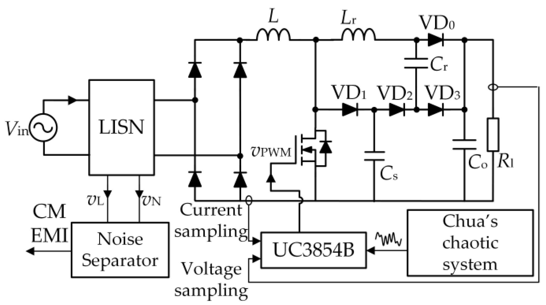
2. Lossless Snubber PFC Converter

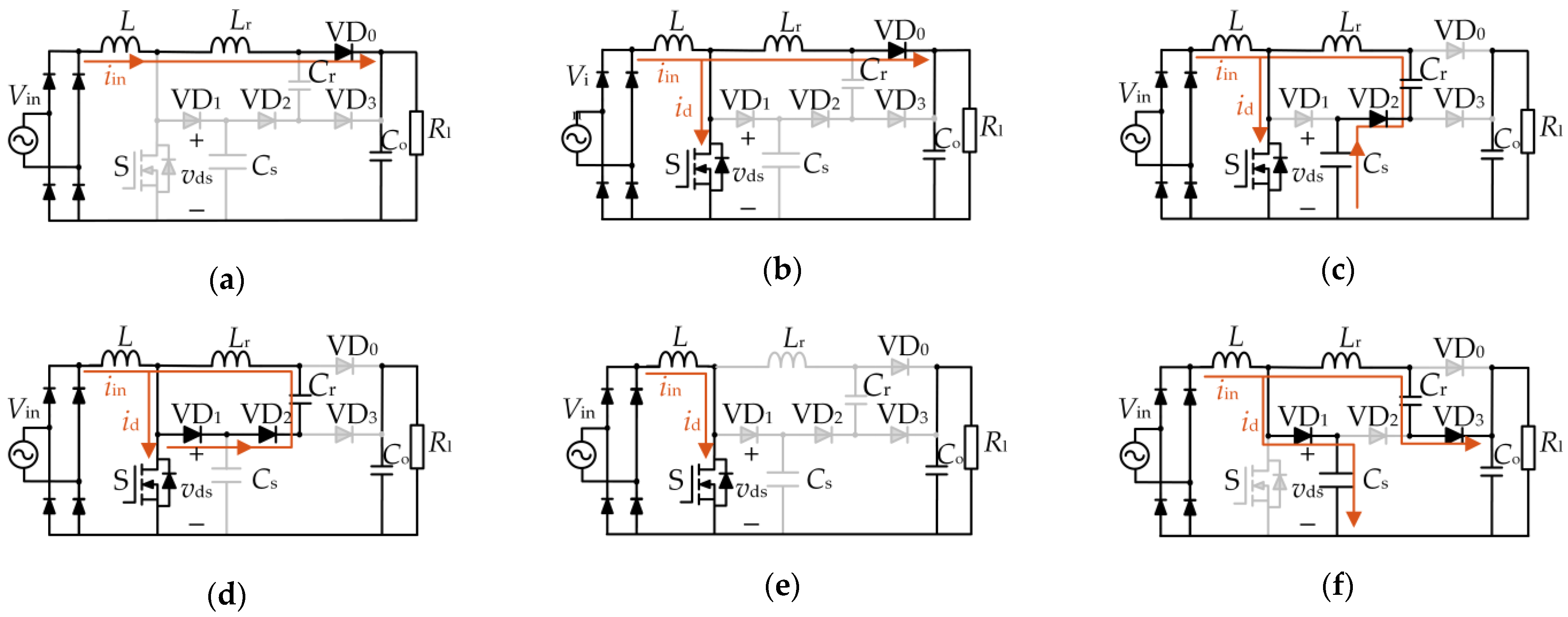
2.1. Principle of the Lossless Snubber

Passive lossless snubber circuits can be used in various power electronic converters. Their structure is relatively universal. CM noise dominates the conducted EMI in slight to medium power Boost PFC converters. This paper, therefore, takes a low-power PFC converter as the object of study. The CM EMI suppression effect of a lossless snubber circuit is analyzed, while other disturbances caused by complex topologies can be reduced.
A Boost PFC converter topology with a passive lossless snubber circuit is shown in Figure 1. Inductor L, switching S, diode VD0, and output capacitor Co form the main circuit of the PFC converter diodes. VD1, VD2, VD3, inductor Lr, and capacitors Cr and Cs in the dashed box form the passive lossless snubber circuit.
The principle of a lossless snubber circuit to reduce the du/dt of the converter is as follows: When the switching is disconnected, the rate of rise of the drain–source voltage (vds) is limited by Cs. Afterward, the lossless snubber circuit transfers the energy from the snubber circuit to the load by resonance, and its operating modes are shown in Figure 2. In mode 1, the switch is in the off-state, the same as when switched off in a conventional PFC converter. In mode 2, the switch turns on, and the current flowing through Lr decreases linearly. Because the switching frequency is much greater than the operating frequency, the input current iin can be approximated as constant over one switching cycle. Then, the drain–source current id starts to rise linearly. Lr has a significant impact on mode 2. A large Lr can reduce the rising rate of id. However, too large Lr will make mode 2 last too long and affect the whole process of the lossless snubber circuit. In mode 3, diode VD0 turns off, and VD2 turns on after the current flowing through Lr drops to zero. Cs, Cr, and Lr start the first resonance process. The energy on Cs is gradually transferred to Cr and Lr in this mode. Mode 3 ends when the energy transfer in Cs is complete. In mode 4, the voltage across Cs drops to zero. At this time, VD1 is on. In addition, Cr and Lr carry out the second resonance process through VD1 and VD2. The energy on Lr is transferred to Cr. When the energy transfer in Lr is completed, mode 4 ends. In mode 5, the second resonance process ends. This mode coincides with the conventional PFC converter when the switching is on. The energy of the snubber circuit is stored in Cr. In mode 6, the switching is off. However, vds cannot change rapidly due to the presence of Cs. Cs limits the rising rate of vds. Cs plays a significant role in this mode. A suitable value of Cs can effectively reduce du/dt. Nevertheless, too large a Cs can affect the resonance process and reduce the stability of the converter. Meanwhile, in mode 6, VD3 conducts. The energy in Cr is transferred to the load, which realizes the lossless operation of the lossless snubber circuit.
The operating principle of the lossless snubber circuit shows that the snubber circuit mainly relies on the snubber capacitor to suppress the du/dt of the switching tube. Because the lossless snubber circuit can transfer the energy from the snubber circuit to the load through resonance, its opening loss is smaller than that of the conventional snubber circuit. Therefore, without affecting the regular operation of the converter, the lossless snubber circuit can choose a larger capacitance snubber capacitor to obtain a better du/dt suppression effect.

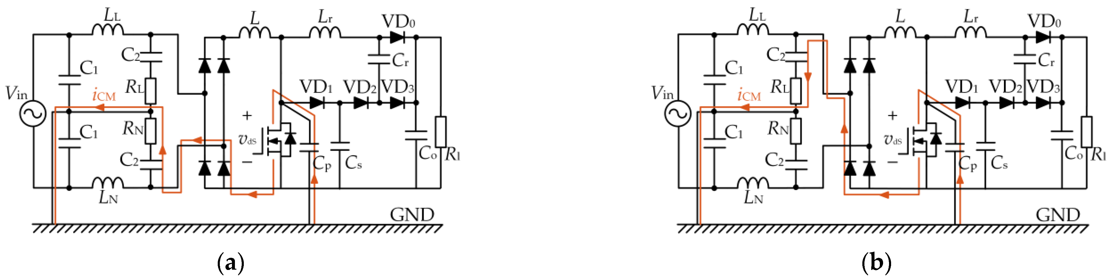
2.2. Equivalent Model of CM EMI

To clarify the impact of du/dt on the CM EMI, the CM EMI conduction path of the lossless snubber PFC converter was first analyzed. When using the linear impedance stabilization network (LISN) for EMI measurements, the CM EMI conduction path is shown in Figure 3.
According to Figure 3, during switching, the high-speed jump of vds forms a CM noise conduction loop through the parasitic capacitance Cp between the switch heat sink and the protective ground. Moreover, the CM current iCM causes CM EMI through the noise conduction loop.
In order to quantify and analyze the principle of nondestructive snubber circuits to suppress CM EMI, the CM EMI conduction loop is equated. The voltage across the LISN resistor was used to measure the magnitude of the CM EMI. We denoted the voltage of resistor RL on the L line as vL and the voltage of resistor RN on the N line as vN. The CM noise voltage vCM can be quantified as:
v CM = ( v L + v N ) / 2
Because Cp is usually very small, its value is only a few tens of pF, and C1 = 1 μF and C2 = 0.1 μF in LISN. Therefore, the CM noise equivalent circuit can be obtained by combining Equation (1) with the conduction path of CM EMI, as shown in Figure 4. In this figure, RLN = RL/2 = RN/2 = 25 Ω. As shown in Figure 4, the high-speed jump vds is the primary noise source of CM noise. So, suppressing du/dt can directly reduce CM EMI.

2.3. CM EMI Suppression Effect of Snubber Circuit

As vds is the primary source of CM noise, the analysis of the CM EMI suppression effect of the snubber circuit can be equated to the analysis of the effect of the snubber circuit on the vds spectrum. The vds waveform is usually approximated as a trapezoidal waveform to simplify the analysis. Decomposing vds into Fourier steps, the amplitude of each harmonic can be obtained as:
A ( k ) = 2 A t τ w f s sin c ( k π f s τ w ) sin c ( k π f s τ r )
In Equation (2), k = 1,2,3, …, denotes the number of harmonics. The function A(k) represents the amplitude of the kth harmonic. The function sinc(x) = sinx/x. At is the amplitude of the trapezoidal wave; fs is the switching frequency; τw is the time between the voltage rising to At/2 and falling to At/2, and τr is the rise and fall time of the voltage.
Due to the fast switching speed of the power-switching devices, the drain–source voltage’s rise and fall times are short. So, there is τw >> τr. According to Equation (2), the envelope of the harmonic amplitude decays with a slope of −20 dB/dec when the number of harmonics is greater than 1/(πfsτw). When the number of harmonics is greater than 1/(πfsτr), the decay slope is −40 dB/dec. Increasing the snubber capacitance suppresses du/dt and reduces the rate of rise of vds. When the higher harmonics start to decay at a relatively low number of times with a slope of −40 dB/dec, this reduces the CM noise at high frequencies. However, to ensure the converter’s regular operation, the value of the snubber capacitor should not be too large, resulting in a lossless snubber circuit for the relatively low-frequency band of the CM noise suppression effect that is poor.

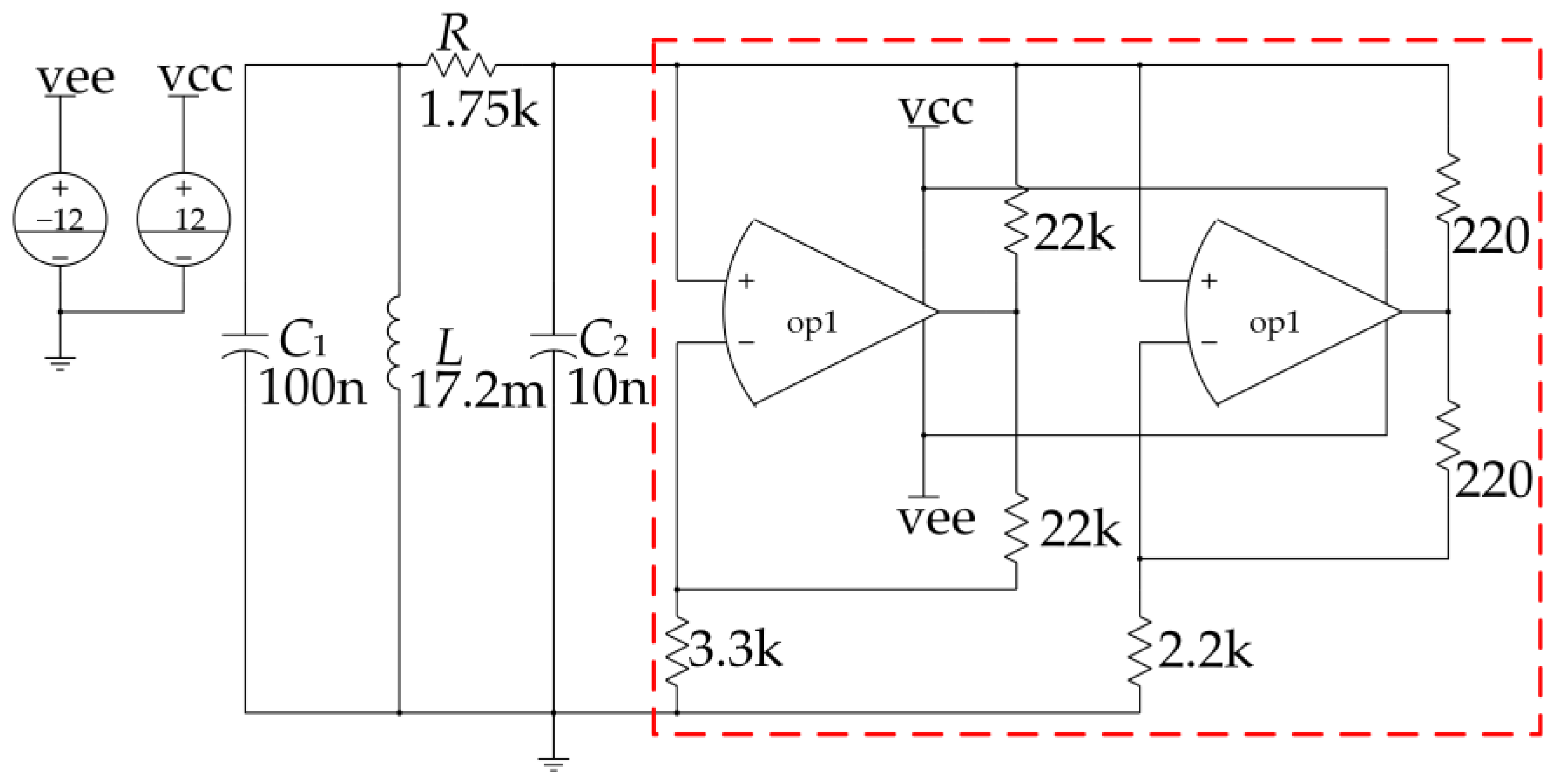
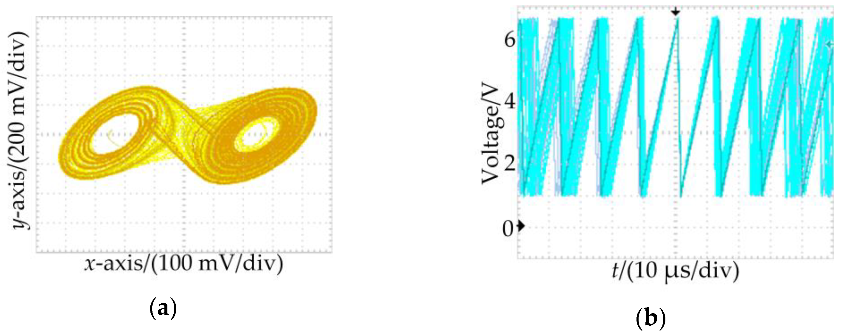
3. Principles of CSS–LS

To improve the low-frequency EMI suppression of the lossless snubber circuit and to further reduce the CM noise of the circuit. The lossless snubber Boost PFC converter was optimized using chaotic spread-spectrum modulation.
Chaos spread spectrum reduces the noise peak at the switching frequency and its multiples by extending the switching spectrum. At the same time, the chaotic spread spectrum has been widely used in various power electronic converters because it does not change the circuit structure or add additional hardware. The key to achieving chaotic spread-spectrum modulation is to make the switching frequency of the switching converter vary chaotically within a specific range. After using chaotic spread-spectrum modulation, the PWM and the drain–source voltage waveforms of the switching are shown in Figure 5.
In Figure 5, Vo is the output voltage amplitude. τn is the starting moment of the nth switching cycle. Tn is the duration of the nth switching cycle. Dn is the duty cycle of the nth switching cycle, and Dn = 1 − Dn. The slope of the voltage rise when the switching tube is switched off was approximated as K. The slope of the voltage fall was approximated as −K.
According to Figure 5, the time domain equation for vds is:
v ds t = n = 1 v ds n t τ n
In Equation (3), vdsn(t) is
v ds n t = Kt , 0   <   t     t 1 V o , t 1   <   t     t 2 V o K t t 2 , t 2   <   t   D n T n 0 , Others
where 0 to t1 is the switching-off process. t1 to t2 is the switching-off time. t2 to D’nTn is the switching-on process, and the slope of voltage rise K = Vo/t1.
Because τn is the accumulation of the first n − 1 switching periods, τn is a chaotic sequence. A time-continuous function N(t) is defined from τn [34]. N(t) denotes the number of vds trapezoidal waves in the time interval [0,t].
N ( t ) = max { n : τ n < t }
For τN(T)TτN(T)+1, the spectrum of vds(t) is:
V ds T j f   = n = 1 N t V ds n j f   e j 2 π f τ n = n = 1 N t V o D n T n t 1 sinc π ft 1 sin D n T n t 1 e - j π f 2 τ n + D n T n
In order to analyze the energy distribution of vds at fundamental and octave frequencies, a replacement representation can be made using the power spectral density. The power spectral density is often used to characterize the distribution of the power of a signal in the frequency domain. The power spectral density P(f) of vds after chaotic spreading is calculated from VdsT(jf) and can be expressed as:
P ( f   ) = lim T 1 T E ( | V ds T ( j f   ) | 2 )
where E(·) is the expectation function.
Substituting Equation (6) into Equation (7), and |VdsT(jf)|2 is calculated as:
V ds T ( j f ) 2 = V o 2 2 π 2 f 2 sinc 2 π f t 1 × N ( t ) i = 1 N ( t ) cos 2 π f D i T i t 1 + i = 1 N ( t ) m = 1 N ( t ) i cos 2 π f Δ τ + Δ T 2 + D i T i D m T m 2 + i = 1 N ( t ) m = 1 N ( t ) i cos 2 π f Δ τ + Δ T 2 D i T i D m T m 2 i = 1 N ( t ) m = 1 N ( t ) i cos 2 π f Δ τ + Δ T 2 + D i T i + D m T m 2 t 1 i = 1 N ( t ) m = 1 N ( t ) i cos 2 π f Δ τ + Δ T 2 D i T i + D m T m 2 + t 1
where ∆τ = τiτm and ∆T = TiTm. Because τn and Tn are chaotic sequences, ∆τ and ∆T are chaotic variations.
Due to the wild and ergodic nature of the chaotic sequences, the double summation term in Equation (8) shows that the distribution of the vds spectrum after spreading is uniform compared to that before spreading. Combining Equation (7) with Equation (8) shows that CSS–LS makes the energy of vds concentrated at the switching frequency, and its multiples are spread over a frequency band with a specific bandwidth. This results in a reduced and continuous peak in the power spectral density of the vds.

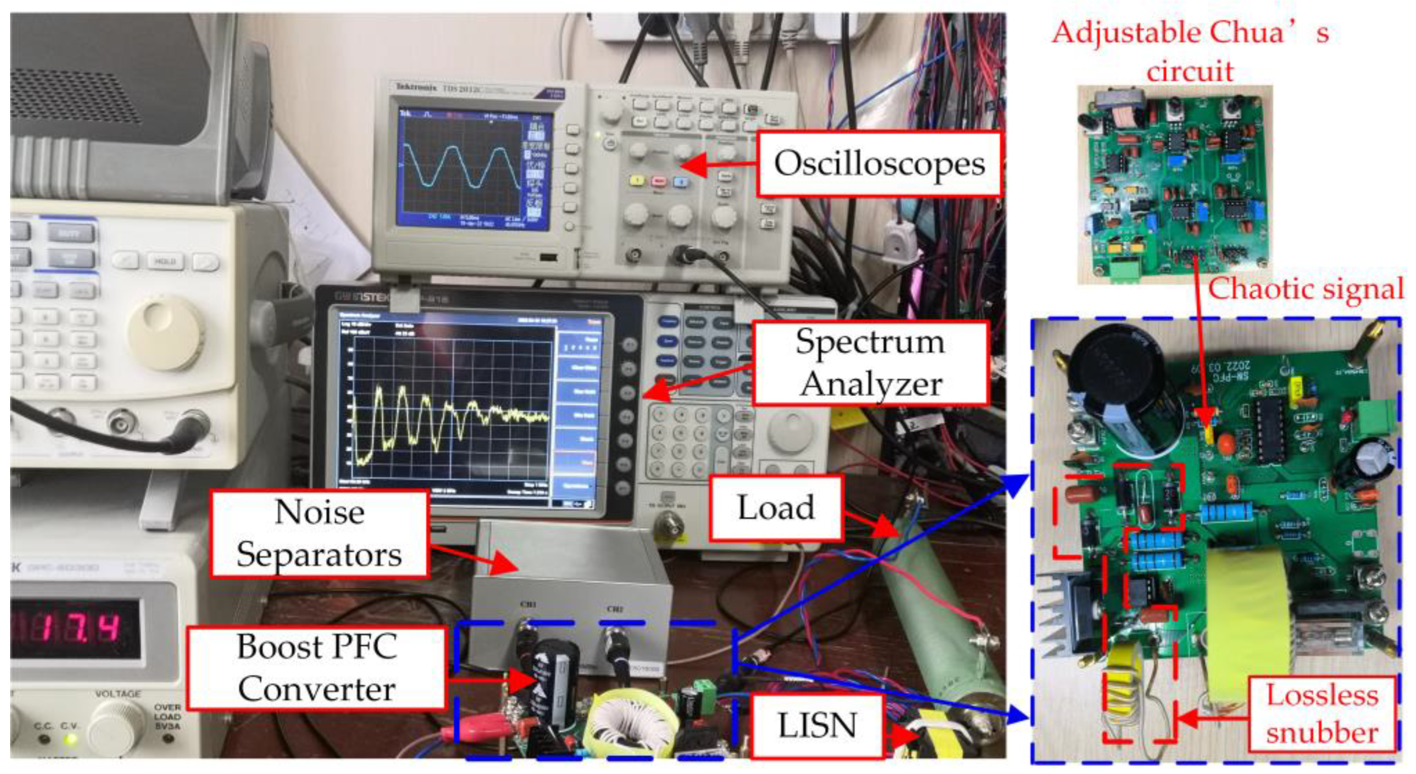
4. Simulation Analysis

In order to verify the accuracy of the above theoretical derivation, this chapter used the simulation software Saber 2016 to simulate the CM EMI suppression effect of the lossless snubber and CSS–LS. A Boost PFC converter simulation model with a lossless snubber circuit was built, and the simulation parameters are shown in Table 1.
UC3854 was selected for the controller of the PFC converter. The switch was selected as IRFP460. Considering the relationship between Cs and switching losses, the value of Cs can be calculated by the following equation [35]:
C sopt = i d R g C dg v g
where Csopt is the optimal value of Cs, Rg is the gate drive resistor, Cdg is the gate–drain parasitic capacitance of the switching tube, and vg is the gate–drive voltage.
After calculations and simulation tests, Cs was taken to be 4.7 nF. The resonant capacitor Cr requires storing the energy of the lossless snubber circuit, and its value is usually 10~30 times that of Cs. The final value of 47 nF was taken for this design.
The analysis of the lossless snubber circuit’s operating mode shows that two resonance processes exist in the lossless snubber circuit. In order to ensure that the resonance process does not affect the regular operation of the converter, the resonance should be completed within the time of the switching tube conduction. Therefore, the resonance parameters need to satisfy the following:
1 2 π L r C r > f s D min 1 2 π L r C eq > f s D min
where Dmin = (1 − Vin_max/Vo) is the minimum duty cycle of the PFC converter, and Ceq = CrCs/(Cr + Cs).
Without affecting the regular operation of the converter, the larger the value of the Lr, the better the buffering effect of the lossless snubber circuit. So, Lr was chosen as 1 μH in this design.
In order to analyze the effect of the lossless snubber circuit, the primary and lossless snubber PFC converters were simulated. The PFC converter was set up according to the Application note about UC3854 from Texas Instruments. The simulation circuit diagram is shown in Figure 6. The chaotic signal for the spread spectrum was generated by Chua’s circuit. Chua’s circuit is a third-order nonlinear circuit. It mainly consists of a linear circuit and a nonlinear circuit. Figure 7 shows a typical Chua’s circuit. In Figure 7, the elements in the dashed box form a nonlinear negative resistor. With correctly set parameters, the voltages across C1, C2, and L vary chaotically.
The simulation set up the probe to measure vds. The corresponding vds waveforms are shown in Figure 8a. According to Figure 8a, the lossless snubber reduces the rising rate of vds and reduces the du/dt of the switching. The spectrum of vds was obtained by fast Fourier transform of the vds waveforms using Saber’s waveform calculator. Moreover, the vds spectrum is shown in Figure 8b. According to the vds spectrum of the conventional circuit and lossless snubber in Figure 8b, we found that the peak of the vds spectrum of both the regular circuit and the lossless snubber (LS) occurs at the switching frequency and its multiples. Furthermore, in the high-frequency band, the peak spectrum of the lossless snubber is lower than that of the basic. This is consistent with the theoretical analysis.
The lossless snubber PFC converter with traditional PWM (TPWM) and chaotic spread spectrum was simulated. Chaotic signals were generated using Chua’s circuit with a spread spectrum of ±10 kHz. Furthermore, the spectrum of vds under TPWM and chaotic spread is shown in Figure 9. The simulation results show that the vds spectrum of CSS–LS has good continuity. The energy of the vds spectrum at the switching frequency and its multiples was dispersed to the surrounding frequencies by using CSS–LS. The energy dispersion reduces the peak value of the vds spectrum with CSS–LS. Compared to the vds spectrum with TPWM+LS, the peak of the vds spectrum with CSS–LS decreases significantly. At 300 kHz~10 MHz, the vds spectrum with CSS–LS is reduced by 6~20 dBµV compared to the vds spectrum of TPWM + LS. The simulation results verify the accuracy of the theoretical analysis, and the chaotic spread spectrum can optimize the EMI suppression effect of the lossless snubber.

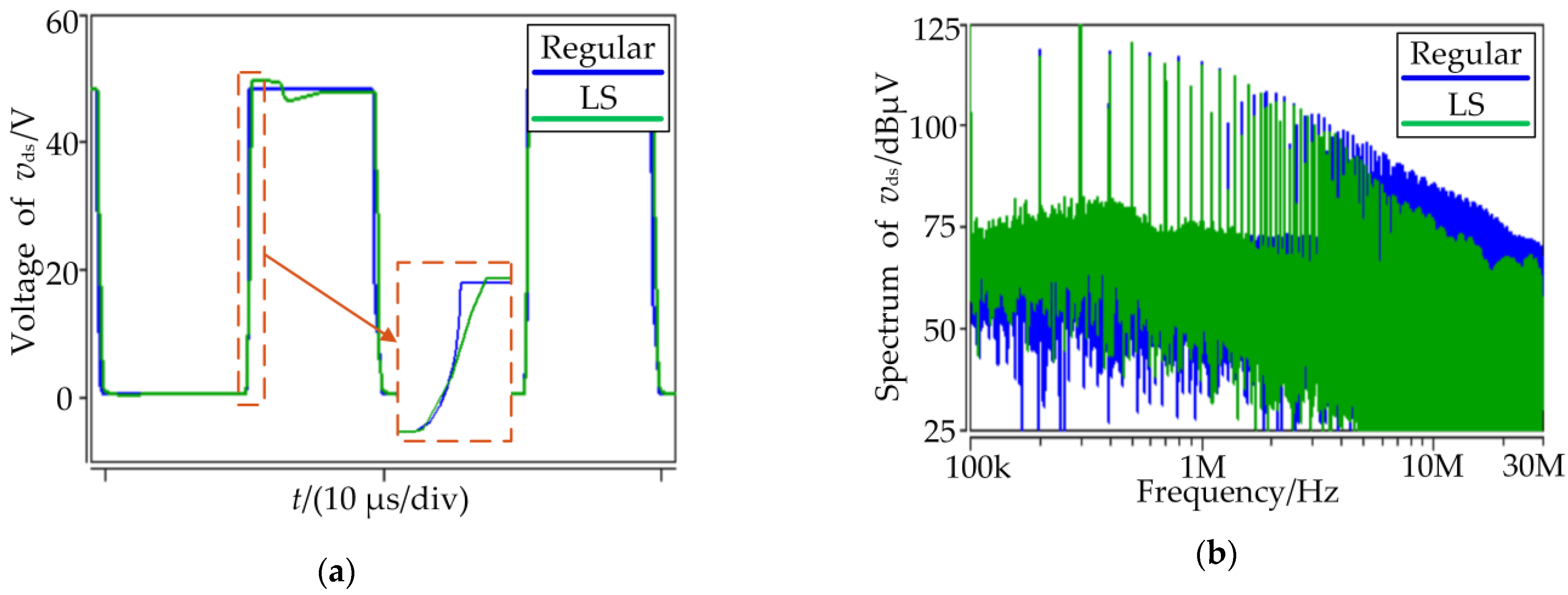
5. Results and Discussion

A prototype Boost PFC converter was built to verify the accuracy of the theoretical derivation and simulation. The experimental circuit diagram is shown in Figure 10. The prototype is shown in Figure 11. The inductor L of the prototype was measured to be 174 µH. The output capacitor Co was selected to be 2200 µF. The load resistance Rl was selected to be 20 Ω. According to the Application note, the UC3854B was set up with a voltage feedback loop and a current feedback loop. Pin 12 of the UC3854B was connected to a resistor Rset, and pin 14 of the UC3854B was connected to a capacitor Ct. The values of Rset and Ct determined the oscillation frequency of the UC3854B. According to the Application note, the switching frequency of the prototype can be derived from the equation fs = 1.25/(Rset × Ct). The switching frequency fs of the prototype was calculated to be about 110 kHz. A programmable power supply provided the input power. The input voltage was 24 V, and the frequency was 50 Hz.
An adjustable Chua’s circuit provided the chaotic signal. The attractor of the chaotic signal is shown in Figure 12a.The waveform of the sawtooth wave delayed by 1 s at Pin 14 of the UC3854 after spreading is shown in Figure 12b, with the switching signal jittering in the time domain.
Firstly, an EMI test was carried out to measure the CM EMI spectrum of the PFC converter in the regular circuit, lossless snubber, and CSS–LS states. LISN was added between the input power supply and the prototype during the test. LISN represents the noise as a voltage. Then, the noise separator separated the CM EMI from the noise voltage. The spectrum of CM EMI was measured by the spectrum analyzer, as shown in Figure 13. The peak value of the CM EMI spectrum at switching frequency multipliers is shown in Table 2.
According to the spectrum of CM EMI, in 0.15~4 MHz, the spectrum of the lossless snubber is similar to that of the regular circuit. The CM EMI suppression effect of CSS–LS can be seen more clearly in Table 2 for the low-frequency band. In the low-frequency band, the CM EMI is not reduced or even higher for the circuit with a lossless snubber than the regular one. In comparison, the CM EMI with CSS–LS is reduced by 6~10 dBµV compared to the regular circuit. In 4~30 MHz, the peak of the CM EMI spectrum of lossless snubber is reduced by 4~10 dBμV. Comparing the CM EMI spectrum of basic circuits with that of CSS–LS, we found that the CM EMI spectrum of CSS–LS has good continuity. In 0.15~4 MHz, the peak CM EMI of CSS–LS is reduced by 6~20 dBμV compared to the basic. In 4~30 MHz, the CM EMI is reduced by 4~20 dBμV.
The experimental results show that CSS–LS significantly improves CM EMI suppression in low frequency compared to the lossless snubber circuits. The suppression effect in the high frequency is also better than that of the lossless snubber. It is consistent with the theoretical derivation and simulation analyses.
Finally, a power supply stability test was carried out. The input voltage, current, and output voltage of the PFC converter were measured under the regular circuit and CSS–LS state as shown in Figure 14. The CSS–LS has a negligible effect on the power factor correction, derived by comparing the input voltage and current sections in Figure 14. As in the conventional circuit, the phase of the input current in the CSS–LS state follows the input voltage very well. The power factor was 99.4% for the regular and 99.4% for CSS–LS. It shows that CSS–LS has less impact on the stability of the Boost PFC power supply.

6. Conclusions

Aiming at the severe problem of EMI in high-frequency switching power supplies, this paper analyses the EMI suppression effect of lossless snubber by establishing a CM EMI model for lossless snubber PFC converters. A proposed CM EMI suppression method combines a passive lossless snubber circuit with a chaotic spread spectrum. This method improves the EMI suppression ability of the lossless snubber circuit at low frequencies. Moreover, it further reduces the peak of high-frequency EMI. At the same time, this method can reduce the switching loss and improve the converter’s efficiency. Furthermore, it does not need to use an auxiliary circuit that is easy to apply. In addition, the CSS–LS only takes up a little space and is lightweight. Therefore, CSS–LS can be integrated into the converter circuit. Using CSS–LS to suppress CM EMI follows the trend of power electronic converters toward high-frequency and high-power density. CSS–LS can be used as an excellent CM EMI suppression method in high-power-density power electronic converters.
The final EMI test results show that CSS–LS reduces the CM EMI amplitude by 6~20 dBμV at a low frequency. The suppression effect in the high frequency is also better than that of the lossless snubber. The power supply stability tests also demonstrate that CSS–LS has little effect on the stability of the Boost PFC converter. Compared with other EMI suppression methods, this method requires fewer changes to the circuit structure and is less costly. The chaotic spread spectrum is suitable for PWM converters that use lossless buffers. This improved method not only reduces CM EMI but also reduces switching losses while taking up less space. This method, which is beneficial to high power density, has certain practical value.

Author Contributions

Conceptualization, W.F. and Y.C.; methodology, W.F.; software, Y.S.; validation, Y.S. and W.F.; investigation, W.F.; data curation, Y.S.; writing—original draft preparation, W.F.; writing—review and editing, Y.C.; project administration, Y.C. All authors have read and agreed to the published version of the manuscript.

Funding

This research received no external funding.

Data Availability Statement

Not applicable.

Conflicts of Interest

The authors declare no conflict of interest.

References

  1. Wang, T.; Kao, Y.; Hung, S.; Wen, Y.; Yang, T.; Li, S.; Chen, K.; Zheng, K.; Lin, Y.; Lin, S.; et al. Monolithic GaN-Based Driver and GaN Switch With Diode-Emulated GaN Technique for 50-MHz Operation and Sub-0.2-ns Deadtime Control. IEEE J. Solid-State Circuits 2022, 57, 3877–3888. [Google Scholar] [CrossRef]
  2. Wang, Y.; Ding, Y.; Yin, Y. Reliability of Wide Band Gap Power Electronic Semiconductor and Packaging: A Review. Energies 2022, 15, 6670. [Google Scholar] [CrossRef]
  3. Tiwari, S.; Basu, S.; Undeland, T.M.; Midtgård, O. Efficiency and Conducted EMI Evaluation of a Single-Phase Power Factor Correction Boost Converter Using State-of-the-Art SiC Mosfet and SiC Diode. IEEE Trans. Ind. Appl. 2019, 55, 7745–7756. [Google Scholar] [CrossRef]
  4. Lee, Y.; Yoo, J.; Hwang, I.; Sul, S. Analysis of Position Estimation Error in Signal-Injection Sensorless Control Induced by Inverter dv/dt-Based Current Measurement Noise. IEEE Trans. Power Electron. 2023, 38, 839–851. [Google Scholar] [CrossRef]
  5. Gao, Z.; Zhang, J.; Huang, Y.; Guan, R.; Zhou, Y. A Closed-Loop Active Gate Driver of SiC MOSFET for Voltage Spike Suppression. IEEE Open J. Power Electron. 2022, 3, 723–730. [Google Scholar] [CrossRef]
  6. Han, L.; Liang, L.; Kang, Y.; Qiu, Y. A Review of SiC IGBT: Models, Fabrications, Characteristics, and Applications. IEEE Trans. Power Electron. 2021, 36, 2080–2093. [Google Scholar] [CrossRef]
  7. Nia, M.S.S.; Shamsi, P.; Ferdowsi, M. EMC improvement for high voltage pulse transformers by pareto-optimal design of a geometry structure based on parasitic analysis and EMI propagation. CSEE J. Power Energy Syst. 2021, 7, 1051–1063. [Google Scholar]
  8. Xie, L.; Ruan, X.; Zhu, H.; Lo, Y. Common-Mode Voltage Cancellation for Reducing the Common-Mode Noise in DC–DC Converters. IEEE Trans. Ind. Electron. 2021, 68, 3887–3897. [Google Scholar] [CrossRef]
  9. Yousef, A.M.; Ebeed, M.; Abo-Elyousr, F.K.; Elnozohy, A.; Mohamed, M.; Abdelwahab, S.M. Optimization of PID controller for hybrid renewable energy system using adaptive sine cosine algorithm. Int. J. Renew. Energy Res. 2020, 10, 670–677. [Google Scholar]
  10. Yap, K.Y.; Beh, C.M.; Sarimuthu, C.R. Fuzzy logic controller-based synchronverter in grid-connected solar power system with adaptive damping factor. Chin. J. Electr. Eng. 2021, 7, 37–49. [Google Scholar] [CrossRef]
  11. Elnozahy, A.; Yousef, A.M.; Ghoneim, S.S.; Abdelwahab, S.A.M.; Mohamed, M.; Abo-Elyousr, F.K. Optimal economic and environmental indices for hybrid PV/wind-based battery storage system. J. Electr. Eng. Technol. 2021, 16, 2847–2862. [Google Scholar] [CrossRef]
  12. Liao, H.; Zhang, X.; Ma, H. Impedance-Shaping-Based Stability Control of Point-of-Load Converter Integrated with EMI Filter in DC Microgrids. IEEE Access 2022, 10, 25034–25043. [Google Scholar] [CrossRef]
  13. Elnozahy, A.; Yousef, A.M.; Abo-Elyousr, F.K.; Mohamed, M.; Abdelwahab, S.A.M. Performance improvement of hybrid renewable energy sources connected to the grid using artificial neural network and sliding mode control. J. Power Electron. 2021, 21, 1166–1179. [Google Scholar] [CrossRef]
  14. Hichem, L.; Amar, O.; Leila, M. Optimized ANN-fuzzy MPPT controller for a stand-alone PV system under fast-changing atmospheric conditions. Bull. Electr. Eng. Inform. 2023, 12, 1960–1981. [Google Scholar] [CrossRef]
  15. Dai, H.; Torres, R.A.; Jahns, T.M.; Sarlioglu, B. Comparative Study of Conducted Common-Mode EMI in WBG-Enabled DC-Fed Three-Phase Current-Source Inverter. IEEE J. Emerg. Sel. Top. Power Electron. 2022, 10, 7188–7204. [Google Scholar] [CrossRef]
  16. Natarajan, S.; Babu, T.S.; Balasubramanian, K.; Subramaniam, U.; Almakhles, D.J. A State-of-the-Art Review on Conducted Electromagnetic Interference in Non-Isolated DC to DC Converters. IEEE Access 2020, 8, 2564–2577. [Google Scholar] [CrossRef]
  17. Zhang, Y.; Li, H.; Shi, Y. Electromagnetic Interference Filter Design for a 100 kW Silicon Carbide Photovoltaic Inverter Without Switching Harmonics Filter. IEEE Trans. Ind. Electron. 2022, 69, 6925–6934. [Google Scholar] [CrossRef]
  18. Kumar, M.; Kalaiselvi, J. Analysis and Measurement of Non-Intrinsic Differential-Mode Noise in a SiC Inverter Fed Drive and Its Attenuation Using a Passive Sinusoidal Output EMI Filter. IEEE Trans. Energy Convers. 2023, 38, 428–438. [Google Scholar] [CrossRef]
  19. Heller, M.J.; Krismer, F.; Kolar, J.W. EMI Filter Design for the Integrated Dual Three-Phase Active Bridge (D3AB) PFC Rectifier. IEEE Trans. Power Electron. 2022, 37, 14527–14546. [Google Scholar] [CrossRef]
  20. Hoffmann, S.; Bock, M.; Hoene, E. A New Filter Concept for High Pulse-Frequency 3-Phase AFE Motor Drives. Energies 2021, 14, 2814. [Google Scholar] [CrossRef]
  21. Han, Y.; Wu, Z.; Wu, D. Hybrid Common-mode EMI Filter Design for Electric Vehicle Traction Inverters. Chin. J. Electr. Eng. 2022, 8, 52–60. [Google Scholar] [CrossRef]
  22. Zhang, Y.; Jiang, D. An Active EMI Filter in Grounding Circuit for DC Side CM EMI Suppression in Motor Drive System. IEEE Trans. Power Electron. 2021, 37, 2983–2992. [Google Scholar] [CrossRef]
  23. Zhou, Y.; Chen, W.; Yang, X.; Zhang, R.; Yan, R.; Liu, J.; Wang, H. A New Integrated Active EMI Filter Topology with Both CM Noise and DM Noise Attenuation. IEEE Trans. Power Electron. 2022, 37, 5466–5478. [Google Scholar] [CrossRef]
  24. Li, H.G.; Gong, S.D.; Liu, J.W.; Su, D.L. CMOS-Based Chaotic PWM Generator for EMI Reduction. IEEE Trans. Electromagn. Compat. 2017, 59, 1224–1231. [Google Scholar] [CrossRef]
  25. Li, H.; Ding, Y.; Zhang, C.; Yang, Z.; Yang, Z.; Zhang, B. A Compact EMI Filter Design by Reducing the Common-Mode Inductance with Chaotic PWM Technique. IEEE Trans. Power Electron. 2022, 37, 473–484. [Google Scholar] [CrossRef]
  26. Ji, Q.; Ruan, X.; Ye, Z. The Worst Conducted EMI Spectrum of Critical Conduction Mode Boost PFC Converter. IEEE Trans. Power Electron. 2015, 30, 1230–1241. [Google Scholar] [CrossRef]
  27. Mohammadi, M.R.; Peyman, H.; Yazdani, M.R.; Mirtalaei, S.M.M. A ZVT Bidirectional Converter with Coupled-Filter-Inductor and Elimination of Input Current Notches. IEEE Trans. Ind. Electron. 2020, 67, 7461–7469. [Google Scholar] [CrossRef]
  28. Mohammadi, M.; Adib, E.; Yazdani, M.R. Family of Soft-Switching Single-Switch PWM Converters with Lossless Passive Snubber. IEEE Trans. Ind. Electron. 2015, 62, 3473–3481. [Google Scholar] [CrossRef]
  29. Lee, S.; Do, H. A Single-Switch AC–DC LED Driver Based on a Boost-Flyback PFC Converter with Lossless Snubber. IEEE Trans. Power Electron. 2017, 32, 1375–1384. [Google Scholar] [CrossRef]
  30. Yano, Y.; Kawata, N.; Iokibe, K.; Toyota, Y. A Method for Optimally Designing Snubber Circuits for Buck Converter Circuits to Damp LC Resonance. IEEE Trans. Electromagn. Compat. 2019, 61, 1217–1225. [Google Scholar] [CrossRef]
  31. Yau, Y.; Hung, T. Lossless Snubber for GaN-Based Flyback Converter with Common Mode Noise Consideration. IEEE Access 2022, 10, 56652–56667. [Google Scholar] [CrossRef]
  32. Wu, Y.; Yin, S.; Li, H.; Ma, W. Impact of RC Snubber on Switching Oscillation Damping of SiC MOSFET with Analytical Model. IEEE J. Emerg. Sel. Top. Power Electron. 2020, 8, 163–178. [Google Scholar] [CrossRef]
  33. Han, W.; Cheng, Q.; Chen, C.; Lee, H. Conductive EMI Reduction Techniques for Soft-switched Half-bridge Buck Converters in Automotive Applications. In Proceedings of the 2022 IEEE Applied Power Electronics Conference and Exposition (APEC), Houston, TX, USA, 20–24 March 2022. [Google Scholar]
  34. Yang, R.; Zhang, B. Experiment and mechanism research of chaotic PWM of converter in EMI suppressing. Proc. CSEE 2007, 10, 114–119. [Google Scholar]
  35. Yu, X.; Su, J.; Guo, S.; Zhong, S.; Shi, Y.; Lai, J. Properties and Synthesis of Lossless Snubbers and Passive Soft-Switching PWM Converters. IEEE Trans. Power Electron. 2020, 35, 3807–3827. [Google Scholar] [CrossRef]
Figure 1. Lossless snubber Boost PFC circuit topology.
Energies 16 03583 g001
Figure 2. Operating modes of lossless snubber PFC: (a) Mode 1; (b) Mode 2; (c) Mode 3; (d) Mode 4; (e) Mode 5; and (f) Mode 6.
Energies 16 03583 g002
Figure 3. Conduction of CM EMI: (a) Positive half-cycle of input voltage and (b) Negative half-cycle of input voltage.
Energies 16 03583 g003
Figure 4. Equivalent circuit of CM EMI.
Energies 16 03583 g004
Figure 5. Waveforms of PWM and drain–source voltage.
Energies 16 03583 g005
Figure 6. Boost PFC converter simulation circuit.
Energies 16 03583 g006
Figure 7. Chua’s simulation circuit.
Energies 16 03583 g007
Figure 8. Drain–source voltage waveforms under regular and lossless snubbers: (a) Drain–source voltage waveform and (b) Drain–source voltage spectrum.
Energies 16 03583 g008
Figure 9. Drain–source voltage spectrum under TPWM and CSS–LS.
Energies 16 03583 g009
Figure 10. Circuit experiment.
Energies 16 03583 g010
Figure 11. Experiment platform.
Energies 16 03583 g011
Figure 12. Chaotic spread spectrum: (a) Chaotic attractor and (b) Sawtooth waveform.
Energies 16 03583 g012
Figure 13. CM EMI spectrum.
Energies 16 03583 g013
Figure 14. Input voltage and current and output voltage waveforms: (a) Regular Boost PFC converter and (b) Boost PFC converter with CSS–LS.
Energies 16 03583 g014
Table 1. Simulation parameters of Boost PFC converter.
ParametersValue
Input Voltage Vin15~24 V
Output Voltage Vo48 V
Inductance L170 μH
Output Capacitance Co2200 μF
Load resistance Rl20 Ω
Switching Frequency fs100 kHz
Table 2. CM EMI spectrum at multiples of the switching frequency.
Frequency/Hz220 k440 k880 k2.2 M6.6 M11 M22 M
Regular/dBμV83.1787.1180.3759.0352.7441.4835.20
LS/dBμV81.5595.8186.4057.6045.6439.8029.45
CSS–LS/dBμV77.2075.9971.0849.8230.8125.5326.32
Disclaimer/Publisher’s Note: The statements, opinions and data contained in all publications are solely those of the individual author(s) and contributor(s) and not of MDPI and/or the editor(s). MDPI and/or the editor(s) disclaim responsibility for any injury to people or property resulting from any ideas, methods, instructions or products referred to in the content.

