Article

Simulation of Boosting Efficiency of GaAs Absorption Layers with KNbO3 Scatterers for Solar Cells

1
College of Physics, Qingdao University, Qingdao 266071, China
2
School of Chemistry and Chemical Engineering, Nanjing University of Science and Technology, Nanjing 210094, China
*
Authors to whom correspondence should be addressed.
Energies 2023, 16(7), 3067; https://doi.org/10.3390/en16073067
Submission received: 17 February 2023 / Revised: 25 March 2023 / Accepted: 26 March 2023 / Published: 28 March 2023
(This article belongs to the Special Issue Emerging Materials for Energy Catalysis)

Abstract

:
In this work, gallium arsenide (GaAs), which has an adjustable band gap and low cost, was adopted as an absorption layer in which KNbO3, having good dielectric, photoelectric, and piezoelectric properties, served as a scattering element for the improvement in absorption efficiency of solar cells. Benefited by the high absorption efficiency of KNbO3, the utilization of the ultraviolet and infrared bands for solar cells can be strengthened. In addition, the ferroelectric and photovoltaic characteristics of KNbO3 enable the realization of decreased thickness of solar cells. Based on the simulation of the shape, width, and period of the scattering element, the effect of the thickness of the scattering element on the absorption efficiency, quantum efficiency, and total efficiency of absorption efficiency was comprehensively simulated. The results show that the absorption layer delivers the optimal performance when using a hexagonal KNbO3 scattering element. The absorption efficiency of the GaAs absorption layer with KNbO3 as the scattering element is increased by 28.42% compared with that of a GaAs absorption layer with empty holes. In addition, the quantum efficiency is maintained above 98% and the total efficiency is 91.59%. At the same time, the efficiency of such an absorption layer is still above 90% when the angle ranges from 0 to 70°. This work provides theoretical guidance for the rational design of solar cells based on photonic crystal structures.

1. Introduction

The solar cell [1,2,3] has received extensive attention due to its widespread application in actual lives. However, there are two urgent problems in the development of solar cells, namely, high cost [4,5,6] and low photoelectric conversion efficiency [7,8]. During the development of solar cells, new materials with low cost and high absorption efficiency need to be explored; in addition, various structures need to be designed to improve the absorption efficiency and photoelectric conversion efficiency of solar cells. The photonic crystal (PC) [9,10], as a material with periodic permittivity, can be introduced into the absorption layer of solar cells by making use of its photonic band gap and slow light characteristics, which can effectively improve the absorption efficiency of solar cells. Such photonic crystal structures have been already applied in the antireflection layers [11,12,13], transmission layers, and absorption layer of solar cells.
In this work, the effect of photonic crystal on the efficiency of the absorption layer was studied. The thickness of photonic crystal is only a few microns, which greatly reduces the cost. Meanwhile, the honeycomb structure of photonic crystal can effectively avoid the reflection of incident light, so that the solar cell can make better use of the incident light. For instance, Amoolya Nirmal [14] et al. used ZnO photonic crystals to improve the absorption efficiency of solar cells by reinforcing the optical trap and increasing the optical path length, thus leading to the increased number of optical carriers. Sergey Eyderman [15] et al. used GaAs square lattices with a thickness of 200 nm as the absorption layer to improve the recovery efficiency of photons and the photoelectric conversion efficiency by up to 30.60%. Zou [16] et al. took the two-dimensional CH3NH3PbI3 perovskite photonic crystal as the absorption layer of solar cells with the scattering elements of an InAs cylinder, enabling a high absorption efficiency of 82.45%. Since the photonic crystals play a very important role in solar cells, it is meaningful to improve the absorption efficiency and photoelectric conversion efficiency of solar cells by utilizing the slow light characteristics of photonic crystals [17]. Our group has designed photonic crystal of a GaAs absorption layer with a thickness of only 0.20 μm [18]. Such a structure is ideal for the filling of quantum dots, which can greatly improve the photoelectric conversion efficiency of the corresponding solar cell.
Recently, Mohammad Ali Shameli et al. [19] introduced photonic topological insulators into the active layer, enhancing light absorption in thin-film solar cells by limiting and capturing sunlight, and thus achieving an improvement in solar cell performance over a wide wavelength range of 400–1100 nm and at an incidence angle of 0–60°. Jeronimo Buencuerpo et al. [20] created photonic crystals with a localized Gaussian ring in reciprocal space and applied this structure to ultrathin GaAs cells with an absorption layer thickness of 260 nm, and the device achieved a total efficiency of 22.35%. Lilik Hasanah et al. [21] used a photonic crystal absorption layer with a radius of 225 nm and a lattice constant of 500 nm to optimize the absorption efficiency to more than 90%. Based on the previous research, the influence of the photonic crystal absorption layer on the absorption efficiency and photoelectric conversion efficiency of solar cells was further studied in this work, and the full use of infrared and ultraviolet bands was made to improve the efficiency of solar cells.

2. Material Selection and Absorption Layer Design

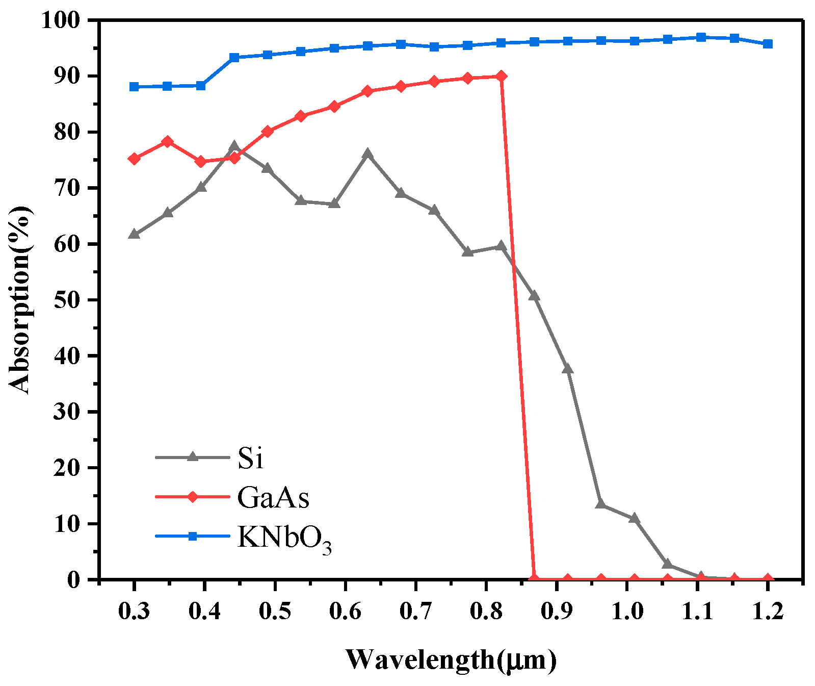
2.1. Material Selection

GaAs has a band gap of 1.40 eV [22], which is compatible with the solar spectrum. Its refractive index varies greatly in the range of 0.30–0.70 μm. The electron mobility of GaAs can reach 8500 cm/(V s) [23], and its carrier lifetime is longer, which is beneficial for photoelectric conversion. In addition, it has a high absorption efficiency of solar energy, together with high temperature resistance and strong plasticity; this, it is the most mature semiconductor material. The absorption efficiency of solar cells will be improved if GaAs is applied in the absorption layer of the cell. In addition, perovskite solar cells [24,25,26] have received increasing attention, with research into Ch3Nh3PbI3 perovskite cells [27,28,29,30], in particular, increasing. However, since Ch3Nh3PbI3 contains toxic elements and poses serious stability issues, it has not been used in practice. KNbO3, as a typical perovskite oxide, has an optical band gap of 1.10–3.80 eV [31,32,33], and possesses good physical and chemical stability. The light absorption of KNbO3 is 3–6 times higher than that of other classical ferroelectric materials, while the optical current density is 50 times that of other classical ferroelectric materials [34]. In addition, the additional electric field in bulk KNbO3 can induce the ferroelectric photovoltaic effect and improve the photoelectric conversion efficiency. The recombination of photogenerated carriers of ferroelectric materials is not affected by the thickness. Conversely, in the traditional P-N junction solar cells, the increasing thickness of the absorption layer is accompanied by the increasing possibility of photogenerated carrier recombination, leading to a low photoelectric conversion efficiency. KNbO3 exhibits fast recombination of photogenerated electrons and holes, high Curie temperature, and good dielectric properties, as well as good photoelectric, piezoelectric, and nonlinear optical properties. KNbO3 is a kind of ferroelectric material with an extra fixed electric field in the matrix and variable polarity, which can produce a ferroelectric photovoltaic effect that exceeds the Shockley–Quesel limit of photoelectric conversion efficiency for current solar cell materials. In addition, KNbO3 can solve the issue of electron–hole pair recombination during the photocatalytic process [35] and improve the photocatalytic activity. From the perspective of environmental protection, KNbO3 is stable against air, thereby improving the stability of the corresponding solar cells and extend the working life of the cells. Scientists from University of Pennsylvania and Drexel University [34] have combined KNbO3 and barium nickel niobate into perovskite crystals, whose absorption efficiency was six times that of the current thin-film solar cell compounds. By adjusting the stoichiometric ratios of perovskite crystal, the band gap can be regulated to realize the application in the field of absorption layers for solar cells. Herein, the two-dimensional GaAs photonic crystal structure is used as a solar absorption layer, and the KNbO3 scatterers are introduced into the above absorption layer in the form of a tetragonal lattice arrangement, which greatly improves the efficiency of the absorption layer. Figure 1 shows the light absorption curves of various semiconductor materials. According to Figure 1, the absorption efficiency of GaAs and KNbO3 is much greater than that of Si material.

2.2. Simulation Methods

Rigorous coupled wave method analysis [36] was used to investigate the optical absorption efficiency and photoelectric conversion efficiency of the absorption layer. The DiffractMOD module in Rsoft software (2018) was used to simulate the absorption efficiency of the optical absorption layer, and the influence of the scatterer’s material, including side length W, lattice constant A, and thickness H, on the optical absorption efficiency was further studied. In addition, here, the type of incident wave was a plane wave, the boundary condition was periodic, the step size was 0.1 µm, and the grid size was 0.005 µm. In order to distinguish the effect of KNbO3 on the absorption efficiency of the absorption layer, the KNbO3 column-type scattering element and the air pore-type scattering element were respectively introduced into perfect GaAs photonic crystal absorption layers for comparison.
The “Solar-Cell” and “DiffractMOD” modules in Rsoft software (2018) were used to calculate the quantum efficiency. The values of parameter W for hexagonal KNbO3 cylindrical and air-hole scattering elements were 0.5 and 0.1 μm. The lattice constants (A) were 1.2 and 0.6 μm. In addition, the values of parameter W for tetragonal KNbO3 cylindrical and air-hole scattering elements were 0.4 and 0.5 μm. The lattice constants (A) were 1.0 and 0.9 μm. The thickness H of scattering element was set as 0.1–1.0 μm in the “Solar-Cell” module. Regarding the “DiffractMOD” module, the type of incident wave was a plane wave, the boundary condition was periodic, the step size was 0.1 μm, and the grid size was 0.005 μm. The simulation range of the wavelength was set as 0.3~1.2 μm with an interval of 0.1 μm. The open circuit voltage was set as 0.7 V. Finally, the quantum efficiency could be obtained by optical and electrical simulation, as calculated by the following equations.
The energy carried by one photon at a wavelength λ is:
E ( λ ) = h v = h c λ [ e V ] ,
where h (4.1357 × 10⁻¹⁵ eV s) is the Planck constant, c (3 × 10⁸ m/s) is the speed of light, and λ is the wavelength. Given a specific incident spectrum S(λ), the total number of photons incident at a wavelength of λ is presented as follows:
n s ( λ ) = S ( λ ) E ( λ ) = λ h c S ( λ ) ,
The total absorption spectrum of the entire device is the sum of the absorption spectra within each layer Ai(λ):
A ( λ ) = i A i ( λ ) ,
These absorption spectra can be computed by DiffractMOD simulation packages. Given these spectra, the number of absorbed photons at a wavelength of λ within each layer is:
n i ( λ ) = S ( λ ) A i ( λ ) E ( λ ) = λ h c S ( λ ) A i ( λ ) ,
The collection efficiencies (ηi) are defined for each absorptive layer. Moreover, it can be useful to consider the shadowing effect of electrodes via another efficiency ηs. The combined number of electron–hole pairs generated at a wavelength of λ and collected by the electrodes is therefore:
n ε h ( λ ) = i η i η s n i ( λ ) = λ h c i η i η s S ( λ ) A i ( λ ) ,
The total number of electron–hole pairs collected by the electrodes is therefore:
N ε h = n ε h ( λ ) d λ ,
Given the parameters defined above, the Quantum Efficiency can be calculated as follows:
Q E ( λ ) = n ε h ( λ ) n s ( λ ) = i η i A i ( λ ) ,
Then the quantum efficiency corresponding to each thickness of the four types of scattering elements is therefore:
Q E H = 0.3 1.2 Q E ( λ ) d λ ,

3. Simulation of Absorption Efficiency for Absorption Layer

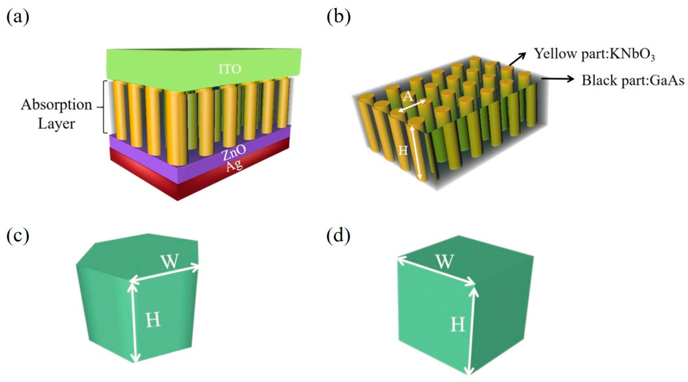
3.1. Absorption Layer Design

The configuration of the solar cell in this work is schematically shown in Figure 2. Figure 2a shows the overall structure of the solar cell, Figure 2b presents the structure of the photonic crystal absorption layer, Figure 2c presents the structure of the hexagonal scattering element, and Figure 2d presents the structure of the square scattering element. The solar cell is composed of an ITO layer, photonic crystal absorption layer, ZnO auxiliary absorption layer, and Ag layer. The optical parameters of each layer of the solar cell are shown in Table 1. Since ~50% of the solar radiation lies in the visible spectrum, most of the current solar cells make use of the visible light, whereas the ultraviolet light with higher energy is not well utilized. The most intense solar energy radiation received on the Earth’s surface is in the range of 300–1200 nm. The rational utilization of this range of light would result in huge economic benefits. Therefore, herein, the incident light in the range of 300–1200 nm was chosen to simulate the absorption efficiency for absorption layer. The active layer is designed as a photonic crystal structure, and the optimal solution of absorption efficiency for the solar cell absorption layer was determined by altering the shapes and parameters of the scatterers in active layer.

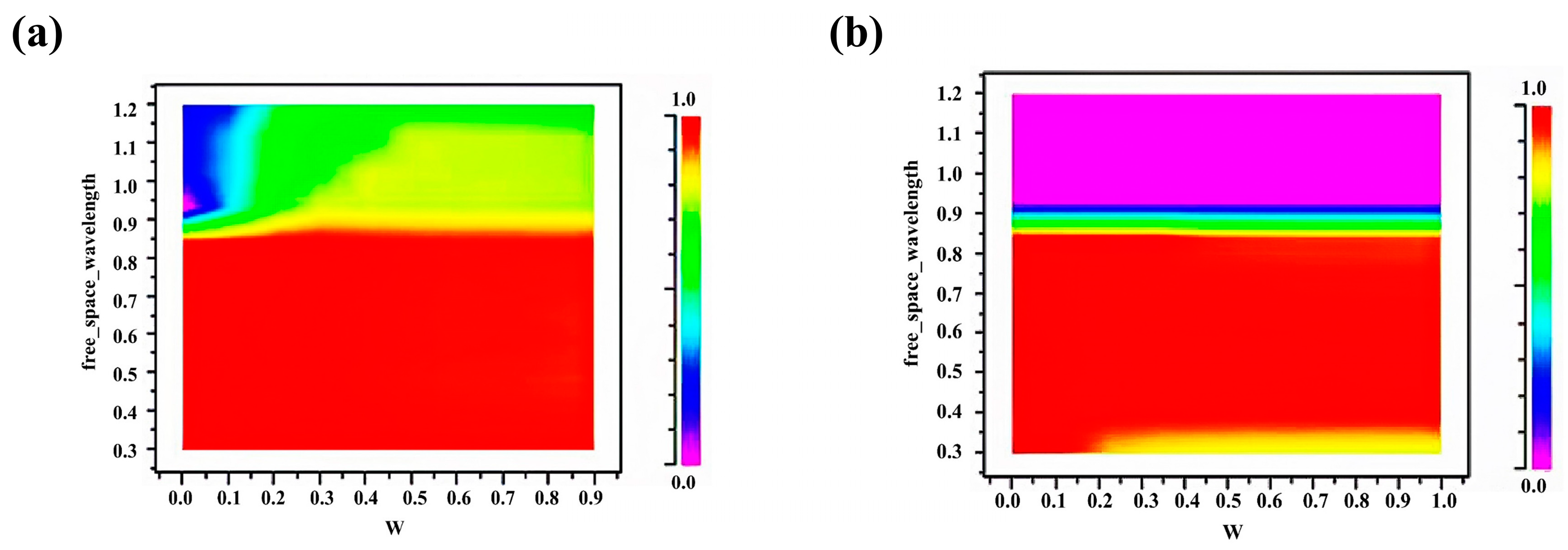
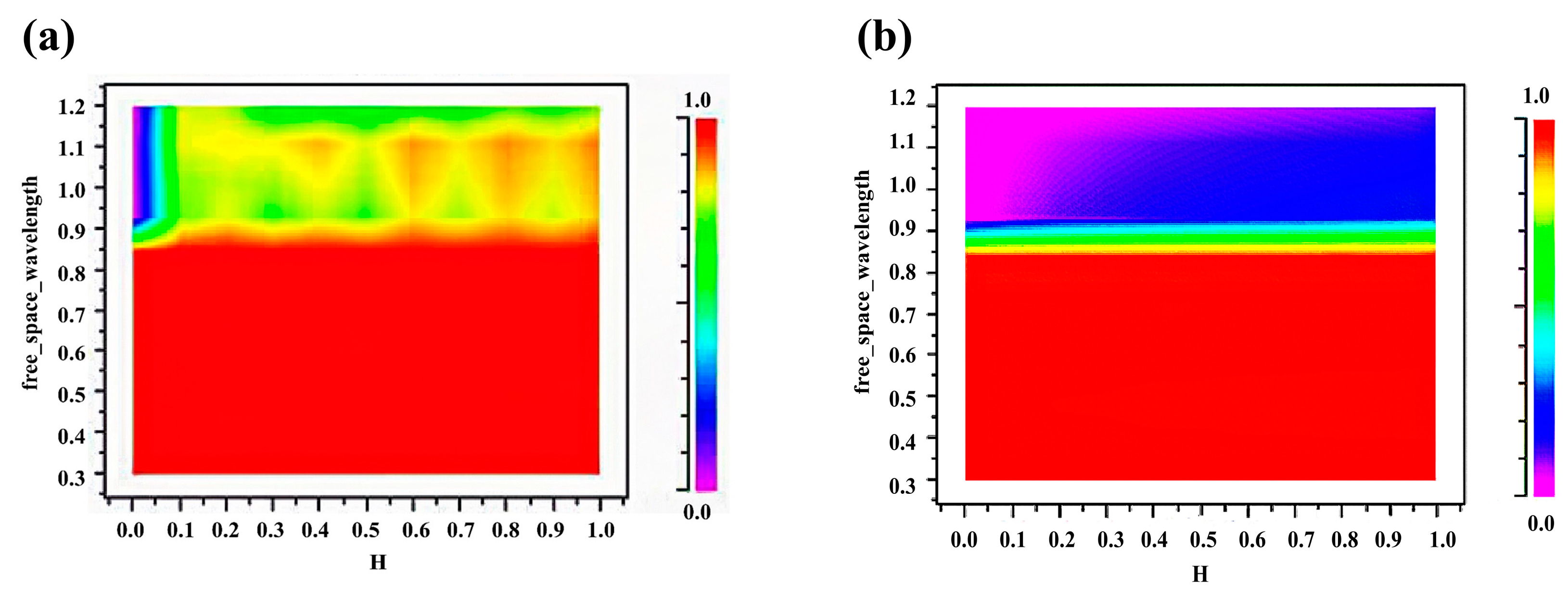
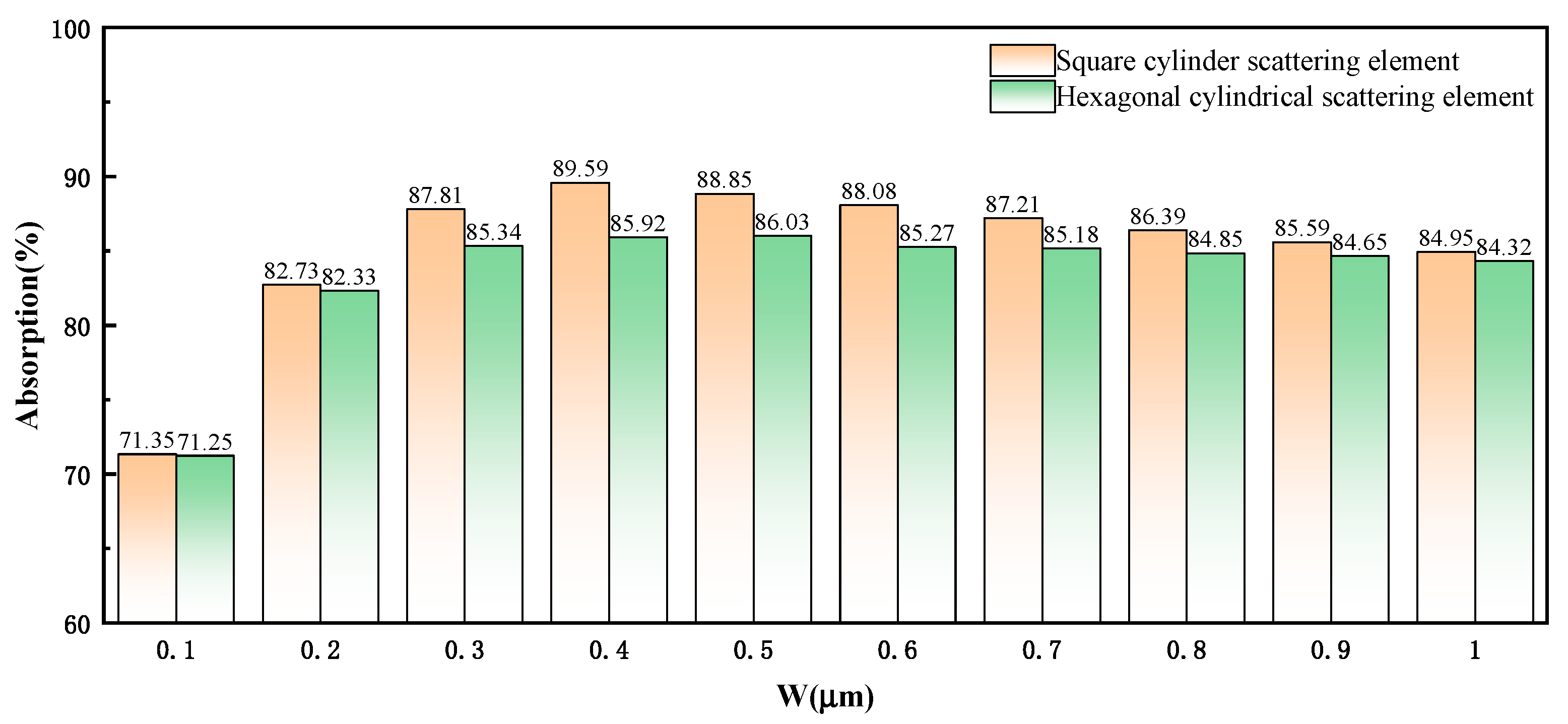
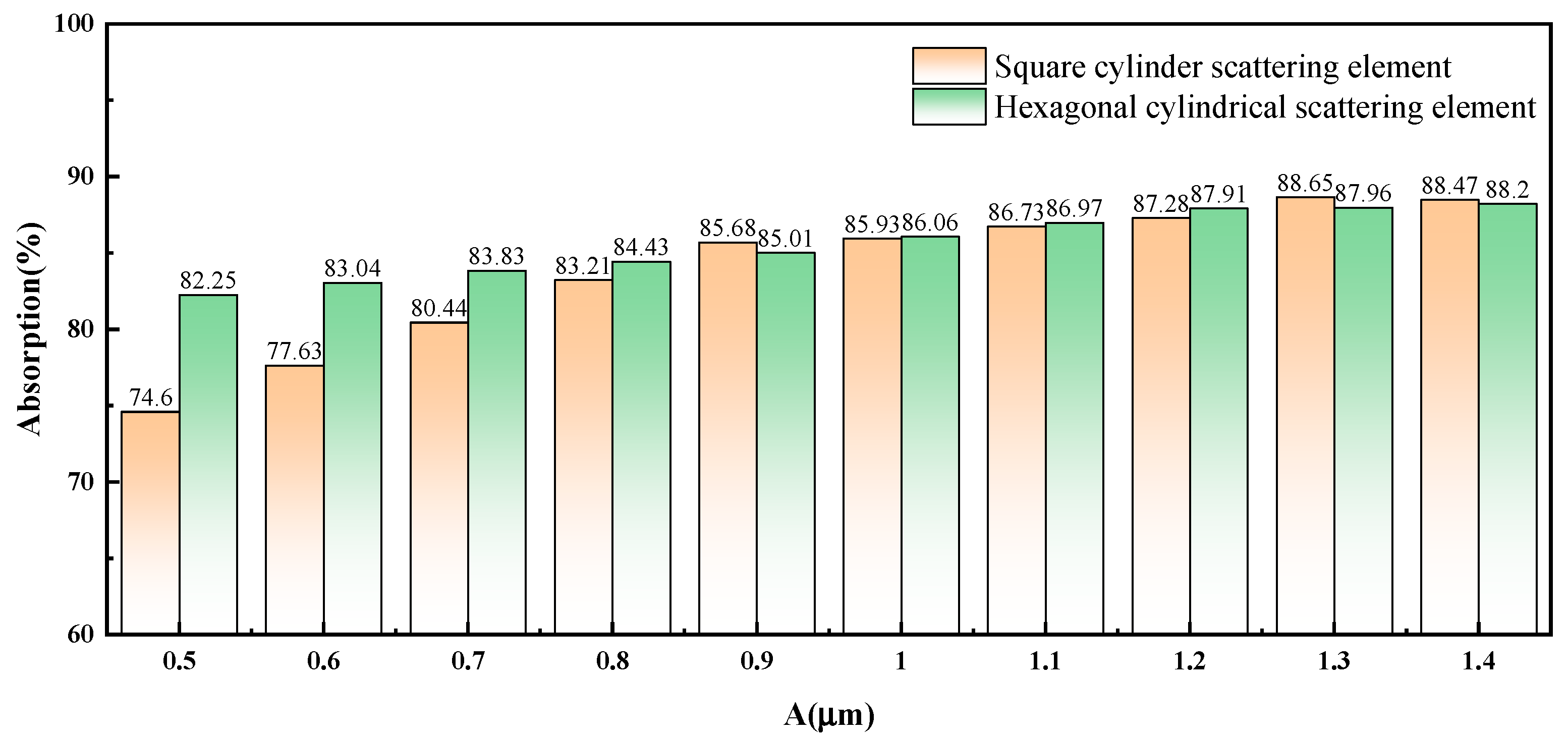
3.2. Hexagonal Scatterers

The hexagon shape is common in nature, including in beehives and turtle shells. The hexagon has excellent stability, and the hexagon structure consumes the least quantity of materials under the condition of a certain volume. Therefore, the absorption efficiency of the absorption layer with hexagonal scatterers was simulated in terms of side length W, lattice constant A, and thickness H. The simulation results of the influence of side length W on absorption efficiency are shown in Figure 3. Figure 3a,b show the dependance of absorption efficiency of the absorption layer with a KNbO3 column and air-hole hexagon scatterers on side length W. The lattice constants A and the thickness H are 1 and 0.5 µm, respectively.
Figure 3a,b show that both the absorption layers exhibit a high absorption efficiency for the light in a wavelength of 0.30–0.80 µm. When the incident light wavelength grows larger than 0.80 µm, the absorption efficiency begins to decrease. The absorption efficiency of absorption layer with KNbO3 column hexagon scatterers decreases when the wavelength is greater than 0.80 µm, but the whole distribution of absorption efficiency lies in the yellow-green region. However, regarding the absorption layer with air-hole hexagon scatterers, the absorption efficiency sharply drops when the wavelength is greater than 0.80 µm, accompanied with the main range in the purple color. The specific results presented in Figure 3a,b are plotted in Table 2.
From Table 2, with the increase in hexagonal lattice side length W, the absorption efficiency of absorption layer with KNbO3 generally presents an upward trend until it reaches the maximum value of 86.03% when W = 0.50 µm. However, the absorption layer comprising an air-hole structure shows a continuously decreasing trend, and the absorption efficiency is about 21.07% lower than that of the former counterpart.
Based on the optimal side length (i.e., W = 0.5 and 0.1 µm, H = 0.5 µm) determined in Table 2, the influence of the lattice constant A on the absorption efficiency was further simulated. If the lattice constant is less than the side length of the scatterers, the scatterers will overlap, which is inconsistent with reality and cannot be applied in practice. Therefore, the absorption layer with KNbO3 cylindrical hexagon scatterers was simulated using the lattice constant A = 0.50 µm. Considering the decreasing tendency of absorption efficiency with the increasing side length for absorption layer with air-hole hexagon scatterers, the simulation started from A = 0.10 µm in this case. The simulation results are shown in Figure 4a,b. Figure 4a,b shows the dependance of the absorption efficiency of the absorption layer with KNbO3 column and air-hole hexagon scatterers on lattice constant A.
Figure 4a,b show that the absorption layer with KNbO3 column hexagonal scatterers delivers a high absorptivity at the wavelength of 0.30–0.80 µm. When the wavelength is higher than 0.80 µm, the absorptivity begins to decay. In addition, the absorptivity increases with the increasing lattice constant. Regarding the absorption layer with air-hole hexagon scatterers, the absorptivity begins to decay at the wavelength of 0.70 µm. When the wavelength is greater than 0.90 µm, the absorption range is dominated by the purple color, and the absorption efficiency is close to 0. To further study the relationship between absorption efficiency and lattice constants, the specific data in Figure 4a,b are presented in Table 3.
Table 3 shows that the absorption efficiency increases with the lattice constant for the absorption layers with both scatterers. The absorption efficiency of the absorption layer with KNbO3 columnar hexagon scatterers slowly increases until the lattice constant A reaches 1.20 µm, while the value of absorption layer with air-hole hexagon scatterers slowly increases until the lattice constant A reaches 0.60 µm. Therefore, the optimal lattice constants for the two cases are determined to be A = 1.20 µm and A = 0.60 µm, respectively.
Based on the optimum parameters (i.e., W = 0.5 and 0.1 µm, A = 1.2 and 0.6 µm) determined in Table 2 and Table 3, the influence of the scatterer thickness H on the absorption efficiency was simulated, as shown in Figure 5. Figure 5a,b show the dependance of the absorption efficiency of the absorption layer with KNbO3 column and air-hole hexagon scatterers on the thickness H.
Figure 5a,b show that the absorption efficiency with KNbO3 column hexagonal scatterers mostly lies in the red, yellow, and green regions, that is, the absorption efficiency is higher than 50%. In addition, the overlapping of three colors occurs at wavelengths larger than 0.80 µm. When the wavelength is greater than 0.90 µm, the absorption efficiency for the absorption layer with air-hole hexagonal scatterers mainly lies in the purple region, indicating the greatly decreased absorption efficiency. To further study the relationship between absorption efficiency and scatterer thickness H, the results of Figure 5a,b are plotted in Table 4.
From Table 4, the absorption efficiency with KNbO3 hexagonal scatterers is ~33.66% higher than that for the air-hole structure. Regarding the absorption layer with air-hole hexagonal scatterers, the absorption efficiency increases with thickness. However, the large thickness introduces the increased possibility of photo-generated carrier recombination, leading to the low photoelectric conversion efficiency. It can be concluded from Table 4 that the thickness H has negligible influence on the absorption efficiency for the absorbing layer with KNbO3 cylindrical scatterers. Thus, considering the cost issue, H = 0.20 μm was selected as the optimal value, corresponding to the absorption efficiency of 92.33%.
From Figure 3, Figure 4 and Figure 5, there is little difference between the efficiencies of absorption layers with a KNbO3 column and air-hole scatterers in terms of the incident light of 0.3–0.9 μm. In the wavelength of 0.9–1.2 μm, the absorption efficiency of absorption layer with KNbO3 column scatterers is much higher than that of the air-hole structure. This indicates that the absorption layer with KNbO3 scatterers exhibits higher light absorption efficiency for long-wavelength incident light, which can be attributed to the spin-induced transitions presented in the metal compounds [34]. The faster the electron transition, the more efficient the light absorption. Compared with air, KNbO3 has no molecules that hinder the flow of electrons, so the electron transition of KNbO3 is faster than that of air, and the absorption efficiency is higher. In addition, KNbO3 has greater absorption bandwidth and higher absorbance compared with air. Specifically, it has six absorption peaks, while air has only one absorption peak; as a result, the absorption efficiency of the KNbO3 absorption layer is significantly higher in the infrared wavelength (0.9~1.2 μm) than that of air.

3.3. Square Scatterers

The absorption of GaAs photonic crystal absorption layers with KNbO3 cylindrical square scatterers or air-hole square scatterers was simulated with adjustments to the side length W, lattice constant A, and thickness H. The simulation results of the effect of side length W on absorption efficiency are shown in Figure 6. The lattice constants A and the thickness H were set as 1 and 0.5 µm.
According to Figure 6, the absorption efficiency of the absorption layer with square and hexagonal scatterers generally shows an upward trend with the increase in side length W, and the value for the absorption layer with square scatterers is slightly larger than that with hexagonal scatterers. In contrast, the absorption efficiency of the absorption layer with square scatterers reaches the maximum value of 89.59% when the side length is 0.40 μm, and decreases with increasing side length W.
Based on the optimal side length (i.e., W = 0.4 and 0.5 µm, H = 0.5 µm) in Figure 6, the effect of the lattice constant on the absorption efficiency for the absorption layer with square scatterers was further simulated. Figure 7 shows the effect of lattice constant A for two different types of scatterers on the absorption efficiency of the absorption layer.
As can be seen from Figure 7, the absorption efficiency of the absorption layer with square scatterers is lower than that of the absorption layer with hexagonal scatterers. In addition, with the increase in lattice constant A, the absorption efficiency for two types of scatterers increases with a gradual slowing trend. Through calculation, the absorption efficiency in terms of square scatterers was found to be 84.12%, while the value for the hexagonal scatterers was 85.60%. The absorption layer with hexagonal scatterers is superior to that with square scatterers.
Based on the optimum parameters (i.e., W = 0.4 and 0.5 µm, A = 1.3 and 1.2 µm) in Figure 6 and Figure 7, the effect of scatterer height on the absorption efficiency for the absorption layer with two types of scatterers is shown in Figure 8. Figure 8 shows the dependance of the thickness H for two different types of scatterers on the absorption efficiency of the absorption layer.
According to Figure 8, the absorption layer with square scatterers generally presents a downward trend, while the absorption layer with hexagonal scatterers presents an upward trend. The absorption efficiency of the absorption layer with hexagonal scatterers is obviously higher than that of the absorption layer with square scatterers. It can be seen from the calculation that the absorption efficiency for square scatterers is 89.75%, while the value for hexagonal scatterers is 91.97%.
Overall, the absorption layer with hexagonal scatterers has higher absorption efficiency than that with square scatterers.

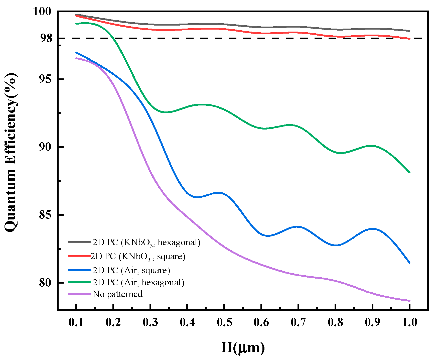
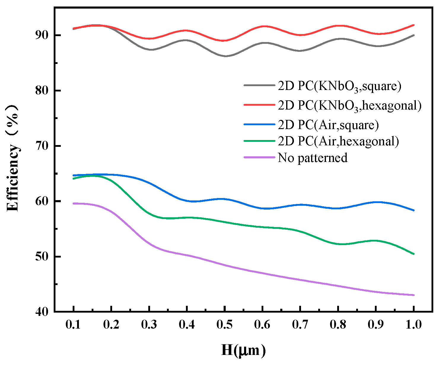
4. Simulation of Quantum Efficiency for Absorption Layer

With the improvement in absorption efficiency, it is also necessary to enhance the photoelectric conversion efficiency of solar cells. Quantum efficiency is a measure that describes the photoelectric conversion capability. The quantum efficiency for a solar cell refers to the ratio of the number of charge carriers in the cell to the number of incident photons with a certain energy on the cell surface. Theoretically, the quantum efficiency of solar cells is associated with the wavelength or energy of incident light. If the solar cell can fully absorb the light with a certain wavelength and produce a minority of carriers, it is considered that the quantum efficiency of solar cell reaches 100%. The photons below the band gap cannot be absorbed by the solar cell, so that the absorption efficiency of solar cell is 0. So, the ideal quantum efficiency image of a solar cell is a square. However, considering the recombination of charge carriers, the practical quantum efficiency of most solar cells is low. The light having short wavelengths is mainly absorbed by the front surface of the solar cell, where the recombination of charge carriers impacts the quantum efficiency of solar cell. The light having long wavelengths is mainly absorbed by the main body of the solar cell. The possibility of carrier combination in the main body increases with the increasing thickness of the solar cell, thus reducing the quantum efficiency of the solar cell. So, the thickness of the solar cell is one of the most important factors that affects the photoelectric conversion efficiency. The introduction of photonic crystals into solar cells presents the following advantages: (1) The photonic band gap can block the photons with certain frequencies from penetrating, thereby increasing the efficiency of photon absorption and collection [16]. (2) The slow light effect results in the significantly decreased group velocity of photons, leading to the markedly improved bandwidth and transmission speed, which is conducive to the excitation of free electrons in the semiconductor and better absorption of photon energy [17]. (3) The introduction of photonic crystal also contributes to the improved electron–hole separation effect and the increased concentration of carriers, thus improving the transport capability of charge carriers [37]. The generally used silicon solar cells are always thick and have a high cost. Instead, in this work, photonic crystals with a thickness of only a few hundred nanometers could be made into thin solar panels, effectively reducing the costs. Moreover, the photoelectric conversion efficiency of traditional Si solar cells is easily affected by the thickness of solar cells, while the absorption efficiency and photoelectric conversion efficiency of photonic crystal solar cells based on GaAs and KNbO3 are very high and are not affected by the thickness. Overall, the total cost of GaAs and KNbO3 based solar cells is less than that of Si based solar cells, while obtaining nearly the same photoelectric conversion efficiency.
In this work, the quantum efficiencies of the four absorption layers with photonic crystal structures and the absorption layer without a photonic crystal structure were simulated, as shown in Figure 9. During the simulation, W and A of the four structures of 2D PC (KNbO3, hexagonal), 2D PC (KNbO3, square), 2D PC (Air, hexagonal), and 2D PC (Air, square) are the optimal values as previously determined (i.e., W = 0.5, 0.4, 0.1 and 0.1 µm, A = 1.2, 1.3, 0.6 and 0.7 µm).
From Figure 9, the quantum efficiencies of absorption layers with different types of scatterers generally decrease with the increase in height. The quantum efficiency of the absorption layer with KNbO3 cylindrical scatterers, which is always above 98%, exceeds that of the other three absorption layers, and it has little change with the increase in height. This indicates that the introduction of KNbO3 photonic crystal can improve the quantum efficiency, and causing the quantum efficiency to be independent of the thickness of the absorption layer. The quantum efficiency of the absorption layer with an air-hole structure greatly varies with the increase in height, but it still exceeds that of the absorption layer without a photonic crystal structure.
In addition, the short-circuit current density (Jsc) is a very important physical quantity in solar cells, and it is an important indicator to measure the photoelectric conversion efficiency of solar cells. This value represents the current density value of a solar cell under the standard light source. The short circuit corresponds to an open-circuit voltage of 0. It can usually be expressed as in Equation (9):
J sc = q 0 Q ( E ) b s d E ,
where q refers to the charge amount, E represents the photon energy, bs is the incident light intensity, and Q(E) refers to the quantum efficiency. Therefore, Jsc is closely related to the light absorption capacity of the absorption layer. The strength of the light absorption capacity directly affects Jsc, thus affecting the photoelectric performance of solar cells. The relationship of Jsc on two different hexagonal scatterers and H is plotted in Table 5. During the simulation, W and A of two structures of 2D PC (KNbO3, hexagonal) and 2D PC (Air, hexagonal) were the optimal values simulated above (i.e., W = 0.5 and 0.1 µm, A = 1.2 and 0.6 µm), and the open circuit voltage was 0.7 V.
According to Table 5, the short-circuit current density of the photonic crystal absorption layer containing KNbO3 is much larger than the absorption layer containing air holes. In addition, in the absorption layer containing air holes, the short-circuit current density generally decreases with the increase in thickness. However, the short circuit density of the absorption layer containing a KNbO3 scattering element is not affected by the thickness. The changing trend and quantum efficiency of the short-circuit current density in the two absorption layers are similar. This can be explained by the introduction of photonic crystals into the solar cell absorption layer. The inherent photon confinement feature reflects the specific light back to the active layer, leading to the reduced light loss. The more light energy absorbed by the active layer, the more electron–hole pairs generated by illumination in the active layer, and the greater the current formed in the solar cell. The increase in light absorption capacity of the active layer significantly improves the short-circuit current density, and then improves the photoelectric conversion efficiency.
The current–voltage curves of the optimal structure (i.e., W = 0.5 µm, A = 1.2 µm, H = 0.2 µm) are plotted in Figure 10a. The open-circuit voltage was 0.7 V. Considering that the filling factor is defined as the ratio of the product of the best bias voltage and the best bias current to the product of the short circuit current and the open circuit voltage, the filling factor of 84.5881% can be calculated. Figure 10b shows the dependance of the total absorption spectrum and quantum efficiency of the absorption layer on the various wavelengths.

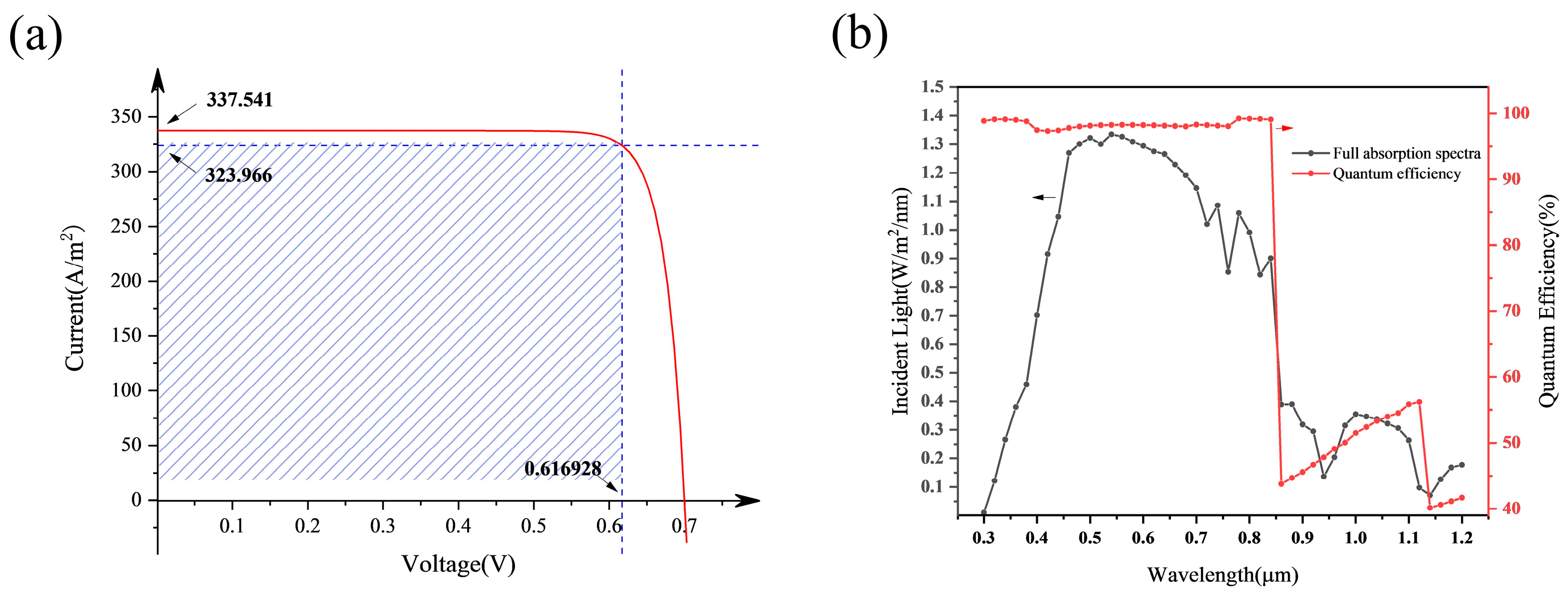
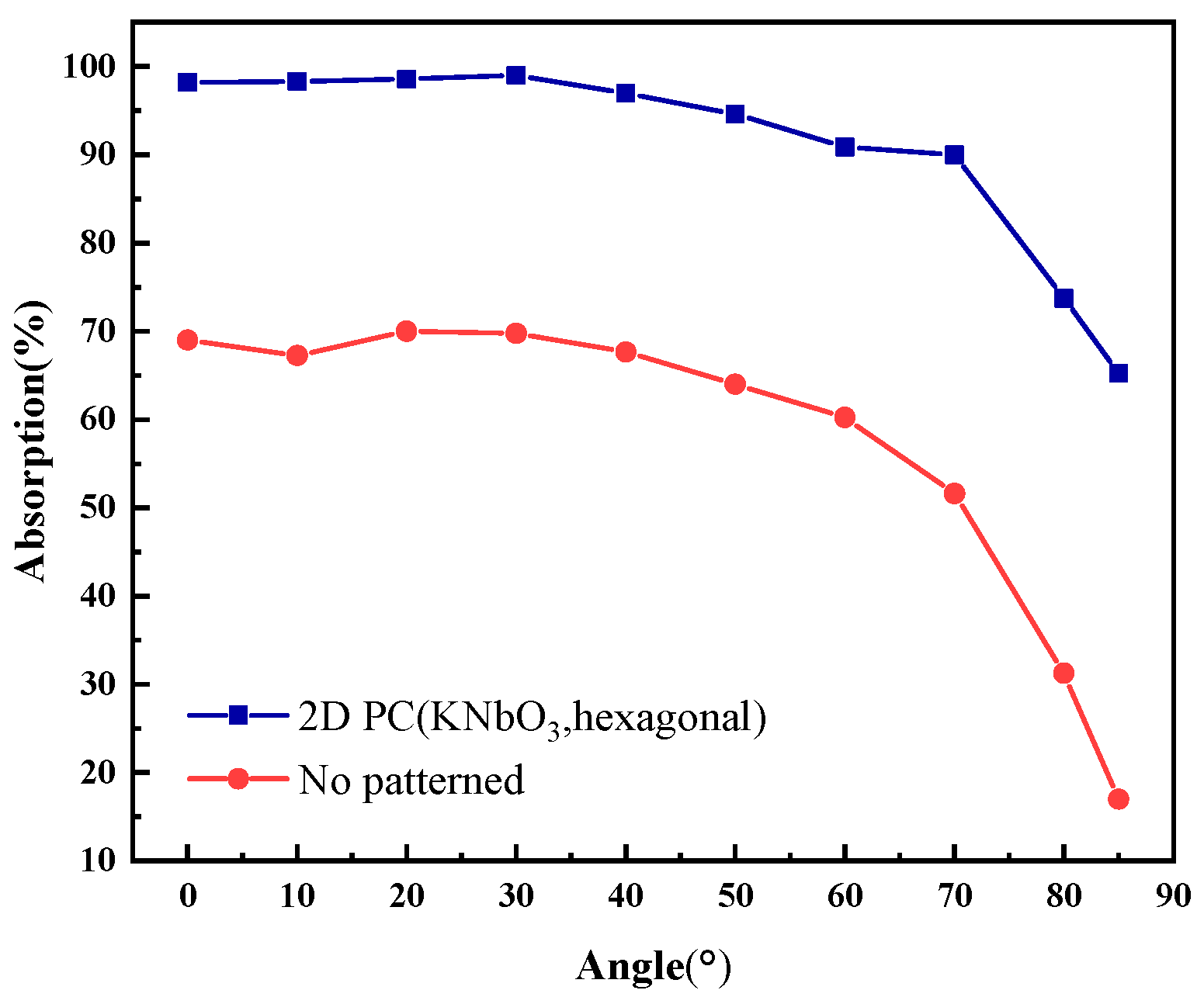
5. Results and Discussion

Firstly, photonic crystal with photonic band gap characteristics and slow light effect was introduced into the absorption layer of solar cells, markedly improving the absorption efficiency. The results indicate that the periodic change in the refractive index induced by KNbO3 and GaAs contributes to the best absorption efficiency of above 90%. Meanwhile, considering the photoelectric conversion efficiency and cost issues caused by the cell thickness, the optimal parameters of absorption layer were selected as the side length W of 0.5 μm, period A of 1.2 μm, and height H of 0.2 μm, achieving an absorption efficiency of 92.33%. By comparison, the optimal absorption efficiency of photonic crystal composed of GaAs and air holes was 64.07%, which is ~30% lower than that of the proposed structure. In order to further study the influence of KNbO3 on the efficiency of solar cells, the simulation results of total efficiency (the product of absorption efficiency and quantum efficiency) for solar cells are displayed in Figure 11. During the simulation, W and A of the four structures of 2D PC (KNbO3, hexagonal), 2D PC (KNbO3, square), 2D PC (Air, hexagonal), and 2D PC (Air, square) were the optimal values as previously determined (i.e., W = 0.5, 0.4, 0.1, and 0.1 µm, A = 1.2, 1.3, 0.6, and 0.7 µm).
As can be seen in Figure 11, the introduction of KNbO3 improves the total efficiency of solar cells to a great extent. The total efficiency of the absorption layer with KNbO3 is far higher than that of the absorption layer with air holes and the absorption layer without a photonic crystal structure. This can be attributed to the superior band gap adjustability and extremely high photocurrent density of KNbO3.
Secondly, the introduction of KNbO3 improves the quantum efficiency of the absorption layer. Unlike traditional solar cells, the quantum efficiency is not affected by the thickness of the absorption layer. This is due to the ferroelectric properties of KNbO3. The absorption layer with KNbO3 photonic crystal is different from the traditional solar cells based on the P-N junction. Regarding the traditional P-N junction solar cells, the built-in electric field is formed based on the depletion layer that separates the photogenerated electrons and hole pairs. However, with the increased thickness of the absorption layer, the recombination possibility of photogenerated carriers increases during the transport process, resulting in the decrease in photoelectric conversion efficiency. In contrast, KNbO3 is a kind of ferroelectric perovskite-type material with variable polarity, which can realize the separation of photogenerated electrons and hole pairs by generating a potential gradient through internal spontaneous polarization [35]. This process does not rely on the P-N junction, so the photoelectric conversion efficiency is no longer limited by the thickness of the absorption layer. On the other hand, most ferroelectric oxides have large photonic band gaps; as a result, ferroelectric oxide based solar cells only utilize a very small part of solar spectrum, thereby limiting the improvement in photoelectric conversion efficiency. However, the direct band gap of KNbO3 can be adjusted within the range of 1.1–3.8 eV, endowing KNbO3 with compatibility with lights in different frequency ranges, thereby improving the photoelectric conversion efficiency. The light absorption properties of KNbO3 can also be regulated by doping transition metal ions. This can make full use of the wide band gap characteristics of KNbO3 photonic crystal, and the band gap can be reduced to a band gap similar to that of visible light, increasing the absorption capability of light and simultaneously increasing the absorption of ultraviolet light.
Thirdly, the absorption efficiency, quantum efficiency, and total efficiency of hexagonal and square scatterers were comprehensively considered. The overall performance of hexagonal scatterers is stronger than that of square scatterers. This is due to the larger light capture area and wider broadband slow light of hexagonal scatterers. The optical loss is the main reason of the low absorption efficiency. Part of the light is reflected from the cell, and it cannot be completely captured by the absorption layer. All these factors reduce the achievable photocurrent from the cell. Therefore, improving the efficiency of solar cells must achieve perfect light capture. Light capture can be achieved by using a photonic crystal. In the presence of periodic patterning with dielectric structures, the guided modes of a thin GaAs slab become leaky and can in- and out-couple to the incoming electromagnetic modes supported by the surrounding medium [38,39]. As a result, the light path length at wavelengths near the band gap in the film is enhanced and the absorption is increased. In addition, when the incident light transports inside the photonic crystal, the media with periodic refractive index will cause very strong scattering of light. This scattering is coupled with the Bragg scattering inside the crystal, resulting in the formation of the photonic band gap. When the frequency of incident light is within the photonic band gap range, this part of light is not allowed to be transmitted inside the photonic crystal. This part of light is reflected, enhancing the interaction between light and matter, and increasing the absorption efficiency. The “slow light” effect slows the group velocity of incident light transmitted inside the crystal. When the incident light wave directly enters the crystal and causes the slow light effect, it will have a greater chance to excite free electrons in semiconductor materials due to the decrease in the group velocity of incident light.
Finally, the absorption efficiency of the incident light at different angles for the absorption layers with a KNbO3 photonic crystal structure and without a photonic crystal structure was simulated, as shown in Figure 12. During the simulation, W and A of the 2D PC (KNbO3, hexagonal) were the optimal values as previously determined (i.e., W = 0.5 µm, A = 1.2 µm, H = 0.2 µm).
From Figure 12, the absorption efficiency of absorption layer with KNbO3 photonic crystal is much higher than that without photonic crystal. Although the absorption efficiency of both absorption layers decreases with the increase in the deflection angle of incident light, the absorption layer with KNbO3 photonic crystal maintains absorption efficiency of ~90% even when the deflection angle is 70°. When the deflection angle is in the range of 70 to 80°, the effective area of light decreases with the increase in incidence angle, leading to the obviously reduced absorption efficiency. Therefore, the absorption layer with KNbO3 photonic crystal can adapt to different dip angles, obtaining greater absorption efficiency. At present, the electron beam etching techniques can be used to fabricate micro-nano structures with an accuracy of less than 5 nm. Hence, the photonic crystal structures can be prepared by electron beam etching techniques and vapor deposition technology. In the actual fabrication process, the negative photoresist is needed for the dielectric column photonic crystal structure, while the positive photoresist is needed for the air-hole photonic crystal structure. The different masks should be made according to the specific structures, and the corresponding KNbO3 mask is introduced into the GaAs absorption layer using the processes of gumming, exposure, post-drying, developing, vertical mold, graphic transfer, degumming, etching, etc.

6. Conclusions

In summary, a novel absorption layer with a two-dimensional photonic crystal structure was designed in this work. When the KNbO3 hexagonal scatterers are arranged in a tetragonal lattice form in the GaAs absorption layer with a side length W of 0.5 μm, lattice constant A of 1.2 μm, and height H of 0.2 μm, the maximum absorption efficiency can reach 92.33%. Regarding the practical applications, KNbO3 can be further doped with transition metal ions to enhance its performance. Moreover, the doping cannot change the crystal structure of KNbO3, but it preserves the ferroelectric properties of KNbO3. The transition metal ion doping combines the optimized optical band gap with ferroelectric properties, thereby obtaining high absorption efficiency and photoelectric conversion efficiency.
The significance of this study lies in the introduction of KNbO3 into the absorption layer of solar cells, reducing the influence of thickness on absorption efficiency and photoelectric efficiency. In this way, the quantum efficiency and the adaptation to different angles can be improved. This offers important guidance for the optimization of the absorption layer structure for novel thin-film solar cells.

Author Contributions

Methodology, L.Z.; software, L.Z.; validation, L.Z., Y.W. (Yihua Wu), X.L. and J.Q.; formal analysis, Z.B., F.Y. and Y.W. (Yong Wan); investigation, X.L. and J.Q.; resources, Y.W. (Yong Wan); writing—original draft preparation, L.Z.; writing—review and editing, Z.B. and F.Y.; supervision, Y.W. (Yong Wan). All authors have read and agreed to the published version of the manuscript.

Funding

This research was funded by the Natural Science Foundation of Shandong Province (Grant No. ZR2020MA084, ZR2019MD016), and the National Natural Science Foundation of China (Grant No. 41976173).

Data Availability Statement

The data presented in this study are available on request from the corresponding author.

Conflicts of Interest

The authors declare no conflict of interest.

References

  1. Panchenko, V.; Izmailov, A.; Kharchenko, V.; Lobachevskiy, Y. Photovoltaic Solar Modules of Different Types and Designs for Energy Supply. Int. J. Energy Optim. Eng. 2020, 9, 74–94. [Google Scholar] [CrossRef]
  2. Polman, A.; Knight, M.; Garnett, E.C.; Ehrler, B.; Sinke, W.C. Photovoltaic materials: Present efficiencies and future challenges. Science 2016, 352, aad4424. [Google Scholar] [CrossRef] [Green Version]
  3. Sukhoivanov, I.A.; Guryev, I.V.; Lucio, J.A.A.; Mendez, E.A.; Trejo-Duran, M.; Torres-Cisneros, M. Photonic density of states maps for design of photonic crystal devices. Microelectron. J. 2008, 39, 685–689. [Google Scholar] [CrossRef] [Green Version]
  4. Green, M.A. Third generation photovoltaics: Ultra-high conversion efficiency at low cost. Prog. Photovolt. Res. Appl. 2001, 9, 123–135. [Google Scholar] [CrossRef]
  5. Green, M.A.; Bremner, S.P. Energy conversion approaches and materials for high-efficiency photovoltaics. Nat. Mater. 2017, 16, 23–34. [Google Scholar] [CrossRef] [PubMed]
  6. Kumavat, P.P.; Sonar, P.; Dalal, D.S. An overview on basics of organic and dye sensitized solar cells, their mechanism and recent improvements. Renew. Sustain. Energy Rev. 2017, 78, 1262–1287. [Google Scholar] [CrossRef] [Green Version]
  7. Zhou, L.; Xu, Y.; Tan, S.; Liu, M.; Wan, Y. Simulation of Amorphous Silicon Carbide Photonic Crystal Absorption Layer for Solar Cells. Crystals 2022, 12, 665. [Google Scholar] [CrossRef]
  8. Li, T.; Zou, X.; Zhou, H. Effect of Mn Doping on Properties of CdS Quantum Dot-Sensitized Solar Cells. Int. J. Photoenergy 2014, 2014, 569763. [Google Scholar] [CrossRef] [Green Version]
  9. John, S. Strong localization of photons in certain disordered dielectric superlattices. Phys. Rev. Lett. 1987, 58, 2486–2489. [Google Scholar] [CrossRef] [Green Version]
  10. Yablonovitch, E. Inhibited spontaneous emission in solid-state physics and electronics. Phys. Rev. Lett. 1987, 58, 2059–2062. [Google Scholar] [CrossRef] [Green Version]
  11. Shen, H.; Zhang, R.; Lu, H. Design of An Amorphous Silicon Thin-film Sloar Cell with Absorption Enhancement. Chin. J. Lumin. 2013, 34, 753–757. [Google Scholar] [CrossRef]
  12. Wensheng, L.; Haiming, H.; Yanhua, F.U.; Qin, Z.; Dufang, S.H.I. Design of highly efficient reflector of solar cells based on photonic crystal. Laser Infrared 2011, 41, 885–888. [Google Scholar]
  13. Zhang, W.; Zheng, G.-G.; Li, X.-Y. Design of light trapping structures for light-absorption enhancement in thin film solar cells. Optik 2013, 124, 2531–2534. [Google Scholar] [CrossRef]
  14. Nirmal, A.; Kyaw, A.K.K.; Jianxiong, W.; Dev, K.; Sun, X.; Demir, H.V. Light Trapping in Inverted Organic Photovoltaics With Nanoimprinted ZnO Photonic Crystals. IEEE J. Photovolt. 2017, 7, 545–549. [Google Scholar] [CrossRef]
  15. Eyderman, S.; John, S. Light-trapping and recycling for extraordinary power conversion in ultra-thin gallium-arsenide solar cells. Sci. Rep. 2016, 6, 28303. [Google Scholar] [CrossRef] [Green Version]
  16. Zou, J.; Liu, M.; Tan, S.; Bi, Z.; Wan, Y.; Guo, X. Rational Design and Simulation of Two-Dimensional Perovskite Photonic Crystal Absorption Layers Enabling Improved Light Absorption Efficiency for Solar Cells. Energies 2021, 14, 2460. [Google Scholar] [CrossRef]
  17. Wan, Y.; Fu, K.; Li, C.; Yun, M. Improving slow light effect in photonic crystal line defect waveguide by using eye-shaped scatterers. Opt. Commun. 2013, 286, 192–196. [Google Scholar] [CrossRef]
  18. Wan, Y.; Jiang, C.-Y.; Wang, X.-M.; Liu, H.-N.; Wang, H.; Cai, Z.; Guo, X. Ultrathin and easy-processing photonic crystal absorbing layers to enhance light absorption efficiency of solar cells. APL Mater. 2019, 7, 041113. [Google Scholar] [CrossRef] [Green Version]
  19. Shameli, M.A.; Yousefi, L. Absorption Enhancement in Thin-Film Solar Cells using Integrated Photonic Topological Insulators. In Proceedings of the 2021 29th Iranian Conference on Electrical Engineering (ICEE), Tehran, Iran, 18–20 May 2021. [Google Scholar]
  20. Buencuerpo, J.; Saenz, T.E.; Steger, M.; Young, M.; Warren, E.L.; Geisz, J.F.; Steiner, M.A.; Tamboli, A.C. Efficient light-trapping in ultrathin GaAs solar cells using quasi-random photonic crystals. Nano Energy 2022, 96, 107080. [Google Scholar] [CrossRef]
  21. Hasanah, L.; Ashidiq, A.; Pawinanto, R.E.; Mulyanti, B.; Wulandari, C.; Wiendartun; Zain, A.R.M. Dimensional Optimization of TiO2 Nanodisk Photonic Crystals on Lead Iodide (MAPbI3) Perovskite Solar Cells by Using FDTD Simulations. Appl. Sci. 2022, 12, 351. [Google Scholar] [CrossRef]
  22. Jiang, C.; Wang, X.; Liu, H.; Zhang, F.; Wan, Y. Using Ultra-thin GaAs Photonic Crystal Absorbing Layer to Improve Solar Cell Absorption Efficiency. J. Synth. Cryst. 2018, 47, 2446. [Google Scholar]
  23. Bi, Z.; Huang, W.; Mu, S.; Sun, W.; Zhao, N.; Guo, X. Dual-interface reinforced flexible solid garnet batteries enabled by in-situ solidified gel polymer electrolytes. Nano Energy 2021, 90, 106498. [Google Scholar] [CrossRef]
  24. Qin, X.; Zhao, Z.; Wang, Y.; Wu, J.; Jiang, Q.; You, J. Recent progress in stability of perovskite solar cells. J. Semicond. 2017, 38, 011002. [Google Scholar] [CrossRef]
  25. Shin, D.H.; Heo, J.H.; Im, S.H. Recent advances of flexible hybrid perovskite solar cells. J. Korean Phys. Soc. 2017, 71, 593–607. [Google Scholar] [CrossRef]
  26. Wan, T.; Zhu, A.; Guo, Y.; Wang, C. Perovskite Solar Cells:From High Efficiency to Stability. Mater. Rev. 2017, 31, 16–22. [Google Scholar]
  27. Chen, Y.; Chen, T.; Dai, L. Layer-by-Layer Growth of CH3NH3PbI3-xClx for Highly Efficient Planar Heterojunction Perovskite Solar Cells. Adv. Mater. 2015, 27, 1053–1059. [Google Scholar] [CrossRef]
  28. Duan, Q.; Ji, J.; Hong, X.; Fu, Y.; Wang, C.; Zhou, K. Design of hole-transport-material free CH3NH3PbI3/CsSnI3 all-perovskite heterojunction efficient solar cells by device simulation. Sol. Energy 2020, 201, 555–560. [Google Scholar] [CrossRef]
  29. Heo, J.H.; Im, S.H. CH3NH3PbBr3-CH3NH3PbI3 Perovskite-Perovskite Tandem Solar Cells with Exceeding 2.2 V Open Circuit Voltage. Adv. Mater. 2016, 28, 5121–5125. [Google Scholar] [CrossRef]
  30. Kojima, A.; Teshima, K.; Shirai, Y.; Miyasaka, T. Organometal Halide Perovskites as Visible-Light Sensitizers for Photovoltaic Cells. J. Am. Chem. Soc. 2009, 131, 6050–6051. [Google Scholar] [CrossRef]
  31. Farooq, U.; Chaudhary, P.; Ingole, P.P.; Kalam, A.; Ahmad, T. Development of Cuboidal KNbO3@alpha-Fe2O3 Hybrid Nanostructures for Improved Photocatalytic and Photoelectrocatalytic Applications. Acs. Omega 2020, 5, 20491–20505. [Google Scholar] [CrossRef]
  32. Yamanaka, T.; Okada, T.; Ohi, K.; Nakamoto, Y. Pressure-induced structure change of ferroelectric KNbO3 using SR. Acta Crystallogr. Sect. A Found. Crystallogr. 2005, 61, c466. [Google Scholar] [CrossRef] [Green Version]
  33. Bi, Z.; Sun, Q.; Jia, M.; Zuo, M.; Zhao, N.; Guo, X. Molten Salt Driven Conversion Reaction Enabling Lithiophilic and Air-Stable Garnet Surface for Solid-State Lithium Batteries. Adv. Funct. Mater. 2022, 32, 8751. [Google Scholar] [CrossRef]
  34. Grinberg, I.; West, D.V.; Torres, M.; Gou, G.; Stein, D.M.; Wu, L.; Chen, G.; Gallo, E.M.; Akbashev, A.R.; Davies, P.K.; et al. Perovskite oxides for visible-light-absorbing ferroelectric and photovoltaic materials. Nature 2013, 503, 509–512. [Google Scholar] [CrossRef] [PubMed]
  35. Ping, W.; Wang, G.; Chen, R.; Guo, Y.; Jiang, D. Enhanced visible light absorption and photocatalytic activity of [KNbO3]1-x[BaNi0.5Nb0.5O3-δ]x synthesized by sol-gel based Pechini method. RSC Adv. 2016, 6, 82409–82416. [Google Scholar]
  36. Gomard, G.; Drouard, E.; Letartre, X.; Meng, X.; Kaminski, A.; Fave, A.; Lemiti, M.; Garcia-Caurel, E.; Seassal, C. Two-dimensional photonic crystal for absorption enhancement in hydrogenated amorphous silicon thin film solar cells. J. Appl. Phys. 2010, 108, 123102. [Google Scholar] [CrossRef]
  37. Chu, Z.; Chen, G.; Zhao, X.; Lin, D.; Chen, C. Research progress of photonic crystals in photocatalysis. J. Mater. Eng. 2021, 49, 43–53. [Google Scholar]
  38. Garnett, E.C.; Ehrler, B.; Polman, A.; Alarcon-Llado, E. Photonics for Photovoltaics: Advances and Opportunities. ACS Photonics 2021, 8, 61–70. [Google Scholar] [CrossRef]
  39. Polman, A.; Atwater, H.A. Photonic design principles for ultrahigh-efficiency photovoltaics. Nat. Mater. 2012, 11, 174–177. [Google Scholar] [CrossRef]
Figure 1. The absorption of various semiconductor materials in the wavelength from 0.3 to 1.2 μm.
Energies 16 03067 g001
Figure 2. (a) Schematic structure of the solar cell. (b) Schematic structure of the photonic crystal absorption layer. (c) Schematic structure of the hexagonal scattering element. (d) Schematic structure of the square scattering element.
Energies 16 03067 g002
Figure 3. (a) The dependance of the absorption efficiency of the absorption layer with KNbO3 column hexagon scatterers on side length W. (b) The dependance of the absorption efficiency of the absorption layer with the air-hole hexagon scatterers on side length W.
Energies 16 03067 g003
Figure 4. (a) The dependance of the absorption efficiency of the absorption layer with KNbO3 column hexagon scatterers on lattice constant A. (b) The dependance of the absorption efficiency of the absorption layer with the air-hole hexagon scatterers on lattice constant A.
Energies 16 03067 g004
Figure 5. (a) The dependance of the absorption efficiency of the absorption layer with KNbO3 column hexagon scatterers on thickness H. (b) The dependance of the absorption efficiency of the absorption layer with the air-hole hexagon scatterers on thickness H.
Energies 16 03067 g005
Figure 6. The effect of side length W for two different types of scatterers on the absorption efficiency of the absorption layer.
Energies 16 03067 g006
Figure 7. The effect of lattice constant A for two different types of scatterers on the absorption efficiency of the absorption layer.
Energies 16 03067 g007
Figure 8. The effect of thickness H for two different types of scatterers on the absorption efficiency of the absorption layer.
Energies 16 03067 g008
Figure 9. Quantum efficiencies of absorption layers with different types of scatterers.
Energies 16 03067 g009
Figure 10. (a) The current–voltage curves of the optimal structure. (b) The dependance of total absorption spectrum and quantum efficiency of the absorption layer on the wavelength.
Energies 16 03067 g010
Figure 11. The total efficiency of the absorption layer with different types of scatterers.
Energies 16 03067 g011
Figure 12. The dependance of the absorption efficiency for the two absorption layers on incidence angle.
Energies 16 03067 g012
Table 1. Optical parameters of the materials used in each layer of the solar cell.
LayerMaterialsRefractive IndexExtinction
Coefficient
Transparent conductive layer/electrodeITO1.635–2.0640.002–0.012
Absorption layerGaAs3.485–5.0520.080–2.288
KNbO32.113–2.3170.041–0.220
Auxiliary absorption layerZnO1.935–2.1050.060–0.430
Reflective layer, electrodeAg0.040–1.3400.392–8.699
Table 2. The relationship between absorption efficiency of absorption layers with two different hexagonal scatterers and W.
Parameter W (µm)Absorption of KNbO3 Column (%)Absorption of Air Hole (%)
0.10 71.2564.96
0.20 82.3364.60
0.30 85.3463.30
0.40 85.9263.06
0.50 86.0362.43
0.60 85.2762.18
0.70 85.1862.04
0.80 84.8561.99
0.90 84.6561.95
1.00 84.3261.92
Table 3. The relationship between absorption efficiency of absorption layers with two different hexagonal scatterers and A.
Parameter A (µm)Absorption of KNbO3 Column (%)Parameter A (µm)Absorption of Air Hole (%)
0.50 82.250.10 56.07
0.60 83.040.20 60.52
0.70 83.830.30 62.36
0.80 84.430.40 63.22
0.90 85.010.50 63.81
1.00 86.060.60 64.07
1.10 86.970.70 64.28
1.20 87.910.80 64.42
1.30 87.960.90 64.51
1.40 88.201.00 64.57
Table 4. The relationship between the absorption efficiency of absorption layers with two different hexagonal scatterers and H.
Parameter H (µm)Absorption of KNbO3 Column (%)Absorption of Air Hole (%)
0.10 91.5157.28
0.20 92.3358.67
0.30 90.5858.32
0.40 92.0759.60
0.50 90.2160.53
0.60 93.1060.64
0.70 91.4661.36
0.80 93.4762.06
0.90 91.8964.07
1.00 93.7464.68
Table 5. The relationship of Jsc on two different hexagonal scatterers and H.
Parameter H (µm)The Jsc of 2D PC KNbO3
Hexagonal (A/m2)
The Jsc of 2D PC Air
Hexagonal (A/m2)
0.1349.503266.437
0.2337.541258.303
0.3331.968254.246
0.4349.024253.724
0.5348.038253.956
0.6346.149250.122
0.7346.526250.195
0.8349.181245.524
0.9346.382246.432
1.0346.698241.451
Disclaimer/Publisher’s Note: The statements, opinions and data contained in all publications are solely those of the individual author(s) and contributor(s) and not of MDPI and/or the editor(s). MDPI and/or the editor(s) disclaim responsibility for any injury to people or property resulting from any ideas, methods, instructions or products referred to in the content.

