Article

Numerical Simulation and Optimization of Inorganic Lead-Free Cs3Bi2I9-Based Perovskite Photovoltaic Cell: Impact of Various Design Parameters

1
Department of Mechanical Engineering, Rajshahi University of Engineering & Technology, Rajshahi 6204, Bangladesh
2
Department of Agriculture, Hajee Mohammad Danesh Science and Technology University, Dinajpur 5200, Bangladesh
3
School of Engineering and Technology, Central Michigan University, Mount Pleasant, MI 48859, USA
4
Electrical Engineering Department, Future University in Egypt, Cairo 11835, Egypt
*
Authors to whom correspondence should be addressed.
Energies 2023, 16(5), 2328; https://doi.org/10.3390/en16052328
Submission received: 30 January 2023 / Revised: 23 February 2023 / Accepted: 24 February 2023 / Published: 28 February 2023
(This article belongs to the Special Issue Modeling and Simulation of Solar Cells)

Abstract

:
The lead halide-based perovskite solar cells have attracted much attention in the photovoltaic industry due to their high efficiency, easy manufacturing, lightweight, and low cost. However, these lead halide-based perovskite solar cells are not manufactured commercially due to lead-based toxicity. To investigate lead-free inorganic perovskite solar cells (PSCs), we investigated a novel Cs3Bi2I9-based perovskite configuration in SCAPS-1D software using different hole transport layers (HTLs). At the same time, WS2 is applied as an electron transport layer (ETL). Comparative analysis of the various design configurations reveals that ITO/WS2/Cs3Bi2I9/PEDOT:PSS/Au offers the best performance with 20.12% of power conversion efficiency (PCE). After optimizing the thickness, bandgap, defect density, and carrier density, the efficiency of the configuration is increased from 20.12 to 24.91%. Improvement in other performance parameters such as short circuit current (17.325 mA/cm2), open circuit voltage (1.5683 V), and fill factor (91.66%) are also observed after tuning different attributes. This investigation indicates the potential application of Cs3Bi2I9 as a lead-free and stable perovskite material that can contribute to improving the renewable energy sector.

1. Introduction

Energy demand is rising continuously because of commercialization and industrialization [1,2]. The ongoing investigation of nonrenewable energy resources such as coal, petroleum, and natural gases has been carried out. Researchers have analyzed the severe environmental consequences of exploiting these materials, raising substantial concerns regarding the development of alternative energy supplies [3]. To replace nonrenewable energy resources and meet rising energy demand in an environmentally sustainable manner, the appropriate usage of renewable energy sources has been a major concern in recent years. Among the several potential renewable energy sources, solar energy stands out as a promising renewable energy resource, alongside wind, geothermal, hydropower, ocean, bioenergy, and tidal energy [4,5]. Solar cell production has increased dramatically in recent years as the cost of solar cells has decreased. However, to compete with fossil fuels and become a significant source of energy, the cost of solar cells must be reduced. Therefore, significant efforts have been made to produce innovative solar cell materials, and a new generation of solar cells based on perovskite materials has recently been developed. Due to the low cost of raw materials and the simple production procedure, perovskite solar cells will most certainly have a big influence on the future solar cell industry. This type of cell may also be competitive with natural gas [6].
Perovskite solar cells (PSCs) are an emerging solar technology that has attracted industrial and commercial attention [7]. The perovskite substance has the composition ABX3, A is organic ammonium, such as MA, B is a metal cation (e.g., Pb2+), and X is a halide anion (e.g., I, Br, Cl). In the crystal structure, the A ion is surrounded by eight three-dimensional structures of corner-sharing octahedral BX6 units [8]. This structure is the composition of calcium titanium oxide (CaTiO3) found in 1839 [9]. The first photocurrent of barium titanium oxide (BaTiO3) was observed in 1956 [10]. From 2009 to 2016, PSCs were manufactured from hybrid-halide materials of methylammonium. Perovskite materials perform well in several applications because of their unique properties in photochromic, electrochromic, image storage, switching, filtering, and surface acoustic wave signal processing devices [11,12,13]. The PCE of photovoltaic cells has increased during the last few years of research by more than 30% from previous poor cells, signaling a bright future for commercial solar cells. High mobility, straight bandgap (Eg), long carrier lifetimes, and a high absorption coefficient are just a few of PSC’s standout qualities. Even though PSCs currently have the highest efficiency of approximately 30%, it is possible to further increase the efficiency of halogen-based PSCs, especially for obtaining PSCs with suitable bandgap [14]. On the other side, perovskite/Si tandem cells and perovskite/CIGS tandem cells with photoelectric conversion efficiencies of about 30% have employed the present broadband gap halogen perovskite successfully. Sn-Pb mixed halogen-based PSCs are recently applied as highly efficient perovskite tandem solar cells due to having perfect bandgap [15].
Pb-based organic–inorganic halide perovskites’ simple construction, bandgap adjustability, and PCE above 30% have advanced thin-film solar cell technology [16]. Despite these successes, developing pollutants (Pb) in perovskite solar cells continues to be a significant barrier to commercialization, as toxicity is the major concern with lead-based perovskite solar cell applications. Thus, alternative compounds with similar optoelectronic properties need to be developed. Bismuth possesses an electronic structure like that of lead with the presence of ns2 electrons that exhibit rich structural variety as well as interesting optical and electronic properties [17,18]. The perovskite layer’s organic components also contribute to the solar cell’s instability. In this regard, lead-based organic halide perovskite solar cells are not suitable or preferable for commercialization in industry. Researchers have experimented with lead-free perovskite materials to reduce toxicity, and using inorganic materials to reduce instability has attracted attention as a potential replacement for organic materials [19].
The application of homo-valent materials like Ge2+ and Sn2+ in place of lead-based solar cell components can minimize toxicity. However, when used at room temperature, they decrease the stability and performance of perovskite solar cells [19]. Moreover, short carrier lifespan and high defect density are the major barriers of tin-based PSCs, which are caused due to quick oxidation of divalent tin ions [20]. Different hetero-valent materials were examined and investigated in lab-based experiments for their feasibility and stability for incorporation into perovskite layers. Among those materials, Bi3+ and Sb3+ with stable +3 oxidation phases have received significant attention. Bi3+ has similar optoelectronic qualities to Pb2+ due to their similarity in ionic radius and electronic structure [21]. Cs3Bi2I9 attracted the most attention among different Bi halide-based materials because of its better PCE and greater durability when compared to other Bi-based perovskite materials [22].
In this work, a novel configuration of Cs3Bi2I9-based perovskite solar cell is optimized in SCAPS-1D software with seven different HTLs (CuO, P3HT, PEDOT, CuSCN, CuSbS2, CuI, and Spiro-OMeTAD). The major purpose of this work is to investigate the lead-free inorganic PSCs having higher efficiency with greater stability. WS2 is used as an electron transport material to evaluate the photovoltaic performance of a Cs3Bi2I9-based heterojunction perovskite solar cell. To configure a suitable PSC device, different models for different HTL materials such as CuO, CuI, PEDOT:PSS, CuSCN, CuSbS2, P3HT, and Spiro-OMeTAD are used in the simulation process. In all simulations of different configurations, the same parametric values of ETL (WS2) and absorber layer (Cs3Bi2I9) are considered, facilitating the comparison of different configurations for different HTL materials. After optimizing the perovskite solar cell configuration, the effects of varied thickness, bandgap, defect density, carrier density, temperature, and other parameters on the cell performance to get an optimum device configuration for achieving higher performance such as improved PCE, FF, short circuit current (JSC), and open circuit voltage (Voc) were investigated. Furthermore, the optoelectrical behavior of a PSC device across its interface of different charge transport layers has been thoroughly investigated. Finally, the barriers and future improvement opportunities of the perovskite solar cells are discussed.

2. Methodology

2.1. Simulation Software

An important step to optimize a solar cell device or configuration is the simulation of solar cell device performance, especially when the device is based on a new material system. It is typically better to get an estimate of expected performance and a reliability analysis using such simulations of the proposed solar cell structure before the actual fabrication because making solar cells is a very complicated and time-consuming process. A variety of programs simulate solar cell characteristics based on the device’s input structure, including SETFOS, AMPS, SILVACO ATLAS, COMSOL, Wx-AMPS, and SCAPS-1D. SCAPS-1D is a numerical simulation solution software developed by the Department of Electronics and Information Systems of Gent University (Ghent, Belgium) [23]. The SCAPS mainly simulates device properties by solving three equations: Poisson’s equation, electron/hole transport equation, and recognized continuity equation. The software assists in simulating multiple configurations and provides several batches run to collect data consistently. It also provides a tool for excellent data analysis and displays through collaborative graphical user interfaces.

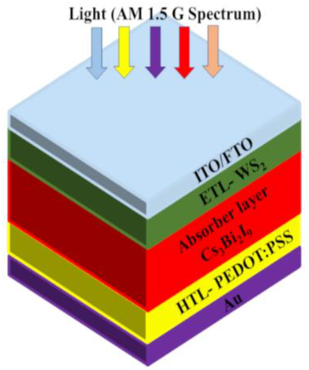
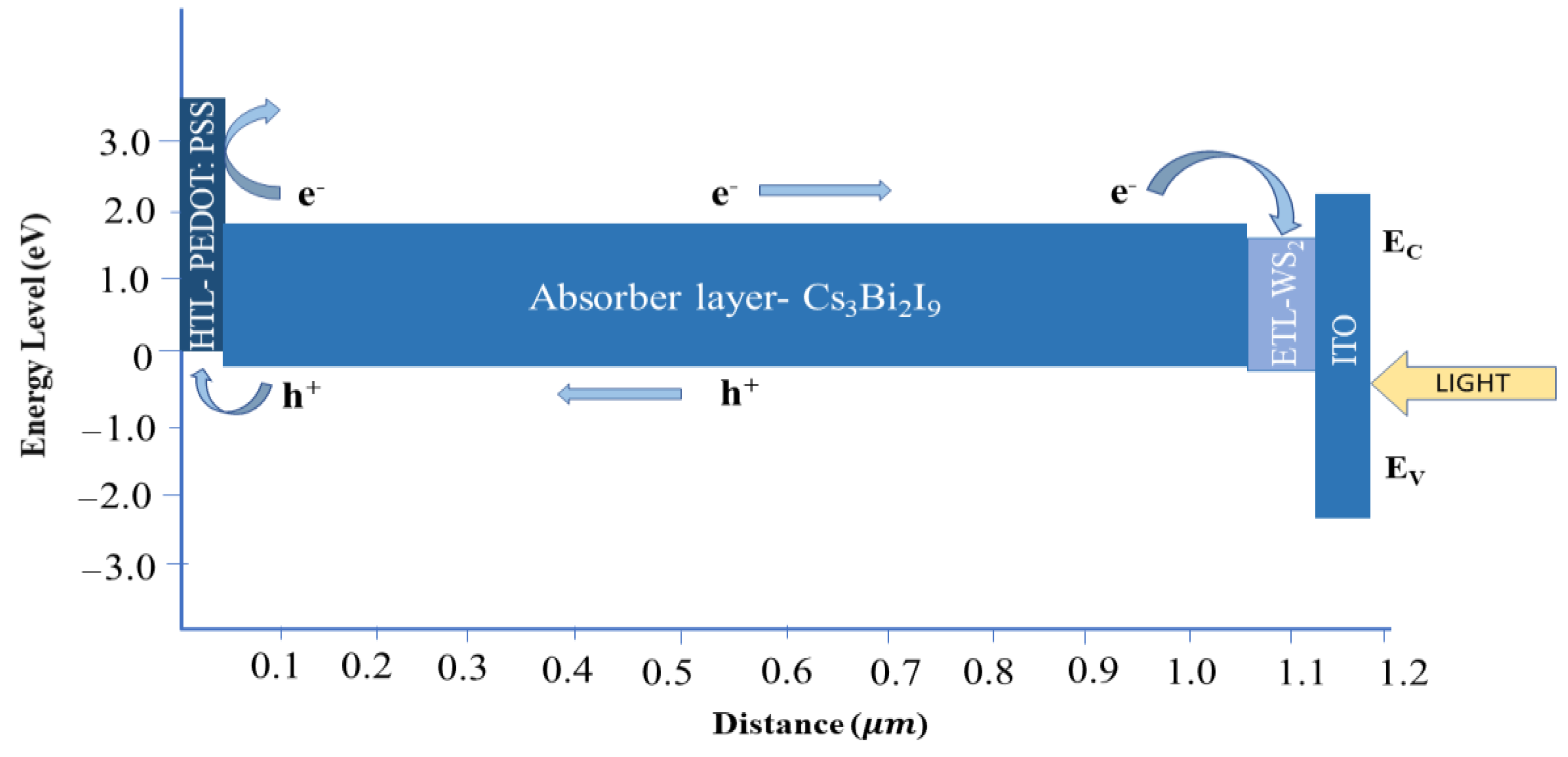
2.2. Modeling and Device Structure

SCAPS-1D software solves the charge carrier continuity equations such as hole continuity Equation (1) and electron continuity Equation (2), the semiconductor Poisson Equation (3) in one direction, total charge transport Equation (4), electron transport Equation (5), hole transport Equation (6) and optical absorption coefficient Equation (7).
d n p d t = G n n p n p 0 τ n + n p μ n d ξ d x + μ n ξ d n p d s + D n d 2 n p d x 2 ,
d n n d t = G p p n p n 0 τ p + p n μ p d ξ d x + μ p ξ d n n d s + D p d 2 p n d x 2 ,
d 2 ( x ) d x 2 = q ϵ o ϵ r p x n x + N D N A + 0.3 ρ p 0.3 ρ n ,
J = J n + J p ,
J n = D n d n d x + μ n n d ϕ d x ,
J p = D p d p d x + μ p p d ϕ d x ,
α λ = A + B h v h v E g ,
where, ξ is the electric field, q denotes electrical charge whose typical value is considered as 1.602 × 10 19 C, ϵ o is the vacuum absolute permittivity, and ϵ r is the semiconductor relative permittivity. ND and NA represent donor doping density and acceptor doping density, respectively. p(x) and n(x) are carrier densities of holes and electrons. ρ p is the defect density of holes and ρ n is the defect density of electrons. Gn and Gp indicate the electron generation rate and the hole generation rate, respectively. Jn and Jp are the hole and electron current densities, respectively. μ n and μ p are electron and hole mobilities. τ n and τ p represent the lifetime of electrons and holes, respectively. Dp and Dn represent diffusion coefficients of free hole and electron. v represents optical frequency, A and B depict arbitrary constants, Eg represents bandgap, h represents Plank’s constant, and α λ depicts the absorption coefficient. Figure 1 shows the configuration of the PSC device, and Figure 2 shows the band energy diagram for our simulated device. The simulated configuration is ITO/WS2/Cs3Bi2I9/PEDOT:PSS/Au where WS2 acts as ETL, Cs3Bi2I9 acts as absorber layer (AL) and PEDOT:PSS acts as HTL.

2.3. Device Input Parameters

In this study, seven HTLs are selected to understand their suitability with WS2 ETL and Cs3Bi2I9 absorber layer. The attributes for all layers have been taken from previously published experimental and simulation works. Temperature, series resistance, shunt resistance, back contact work function, thickness, and defect density has been varied to configure an optimum and maximum device performance. Additionally, the bandgap of Cs3Bi2I9 was tuned from 1.65 to 2.34 eV, and electron affinity was tuned from 3.2 to 3.5 eV based on an experimental investigation of Cs3Bi2I9 [24]. All input parameters of different layers are listed in Table 1.

3. Results and Discussion

3.1. Optimization of HTL

HTL is a crucial element as it is a separator between the absorber layer and the electrode. In addition, it acts as a path to transfer holes generated from the absorber layer. Cs3Bi2I9 is a prospective material to be used as an absorber/perovskite layer in PSC devices for its structural non-toxicity and durability. However, it is hard to find appropriate charge carrier layers for this absorber layer. Additionally, tungsten sulfide (WS2) is considered a suitable electron transport layer that can be employed with Cs3Bi2I9 (absorber layer). Therefore, to fulfill the PSC device configuration, it is required to select an appropriate HTL. For this, different device configurations (ITO/WS2/Cs3Bi2I9/HTL/Au) are simulated and built with various HTL materials such as CuO, PEDOT:PSS, P3HT, CuSCN, Spiro-OmETAD, CuI, and CuSbS2. The study uses identical values for all the parameters of Cs3Bi2I9 and WS2 to simulate the device with different HTLs. Before optimization, the performance parameters were Voc as 1.4355V, Jsc as 16.971 mA/cm2, FF as 82.57%, and PCE as 20.12% when PEDOT:PSS is selected. Table 2 lists the comparison of different performance parameters such as FF, PCE, Jsc, and Voc for various configurations. The best values of these performance parameters are achieved for ITO/WS2/Cs3Bi2I9/PEDOT:PSS/Au. It is clear from the Figure that PEDOT:PSS shows the best performance compared to other HTLs because it has the lowest affinity.

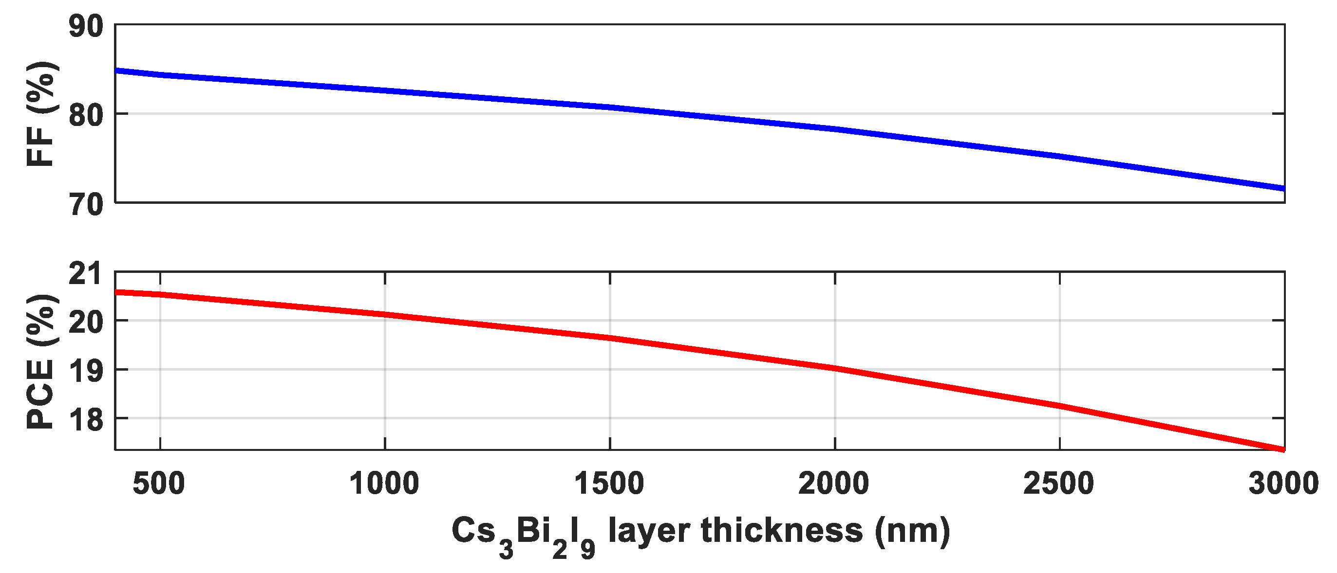
3.2. Effect of Absorber Layer Thickness

The absorber layer (AL) in PSCs is important in evaluating solar cell performance as it absorbs incoming photons and forms charge carriers. The quality of the AL is determined by factors including film shape, which directly affects the durability and diffusion length of photo-generated carriers [42,43]. One of the essential characteristics that contribute to optimizing PSC performance is the thickness of the AL [39]. It should be properly chosen to absorb the highest quantity of photons while not too high to reduce reverse saturation current. To promote PSC performance, the influence of varying absorber thickness between 400 and 3000 nm was evaluated while leaving all other input attributes unchanged. The effect of thickness on the device performance is shown in Figure 3. It can be deduced from Figure 3 that PSCs are more immune to the effect of thickness variations than a-Si [44]. It can be noticed that Voc gradually decreased (1.4368 to 1.4279V) with increasing AL thickness, whereas Jsc increased (16.8866 to 16.975 mA/cm2) gradually with increasing thickness of the AL and then remained constant. In the case of efficiency, PCE decreased from 20.58 to 17.35% with increasing absorber layer thickness from 400 to 3000 nm, whereas FF decreased from 84.83 to 71.58% due to variation in absorber layer thickness. With the increment of AL thickness, the amount of photon absorption increases, for which electron–hole pair generation also increases. As a result, the AL obtained a higher absorption coefficient. However, with increasing AL thickness, the recombination of charge carriers inside the material increases, which causes a loss in efficiency [45]. Therefore, a thickness of 400 nm for Cs3Bi2I9 will be the optimum for high efficiency.

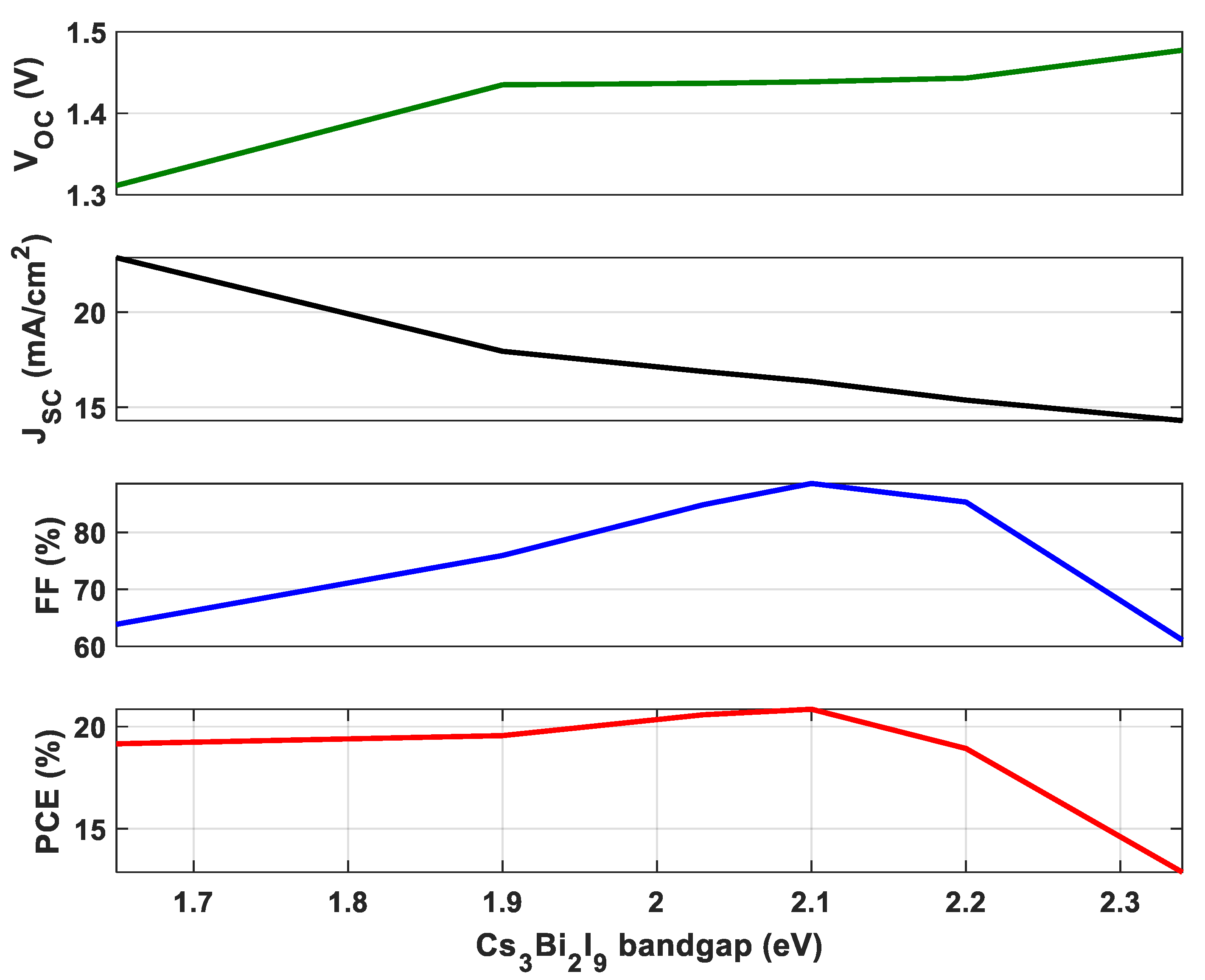
3.3. Effect of Absorber Layer Bandgap

To develop a device with very high performance, optical absorption can be controlled by adjusting the energy band gap of absorber materials [17]. Nonetheless, in a PSC device, the AL’s energy band gap is a crucial element in optical absorption. Previous investigations, simulations, and theoretical calculations have revealed that the Cs3Bi2I9 band gap can be tuned between 1.65 and 2.35 eV. The thickness of Cs3Bi2I9 was set to 400 nm in this case, while the other parameters remained fixed. Figure 4 depicts the variation in device performance parameters as a function of the absorber layer band gap. Figure 4 indicates that, with increasing bandgap, PCE and FF increase gradually and then start to drop down. A maximum of 20.85% PCE can be achieved from this configuration due to an absorber layer bandgap (Eg) of 2.1 eV, and a maximum of 88.56% FF can be obtained, which is also for 2.1 eV bandgap. A dramatic fall in FF (85.29 to 61.12%) and PCE (18.93 to 12.88%) occurs when the Eg is further increased from 2.2 to 2.34 eV. On the other hand, when the device is simulated with a 1.65 eV bandgap, the Jsc value is at the highest point on Jsc characteristic curve. In contrast, for this bandgap, the Voc value is lowest on the Voc characteristic curve. Additionally, for further increase, there would be a slight increase in Voc and a slight decrease in Jsc.

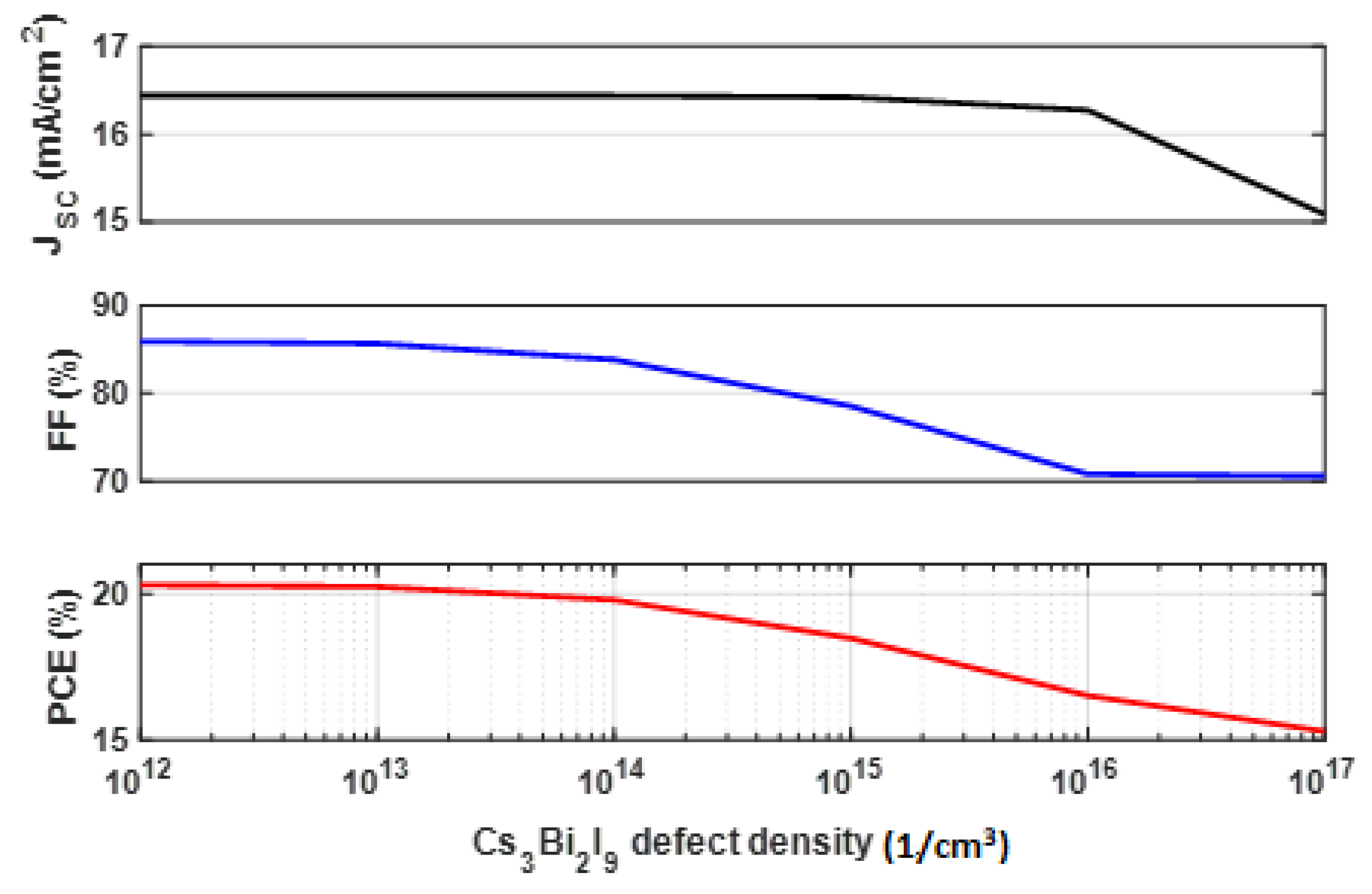
3.4. Effect of Absorber Layer Defect Density

Any perovskite material will inevitably have defects, which can appear as point flaws like vacancies, interstitials, Schottky, and Frankel flaws both in bulk and on surfaces. Additionally, other defects, such as dislocation and grain boundaries, may be discovered [46]. In the perovskite layer, impurity defects can also be produced by the self-doping method, which traps charge carriers and encourages non-radiative recombination [43]. In addition, a large defect density lowers the PSC performance [47]. For a proper understanding of the influence of the defect density of AL, optimization has been carried out at varying AL’s defect densities ranging from 1012 to 1017 cm−3. The effects of absorber layer defect density can be shown in Figure 5. Voc almost remains the same. In the case of Jsc, it remains unchanged with increasing absorber layer defect density, and for further increase in defect density from 1016 to 1017, the Jsc falls from 16.2726 to 15.0879 mA/cm2. Due to the increase of defect density from 1012 to 1017, a gradual decrease can be seen from the graph for both FF and PCE. The graph reveals that FF decreases from 85.88 to 70.56%, and PCE decreases from 20.29 to 15.29%.

3.5. Effect of Carrier Density

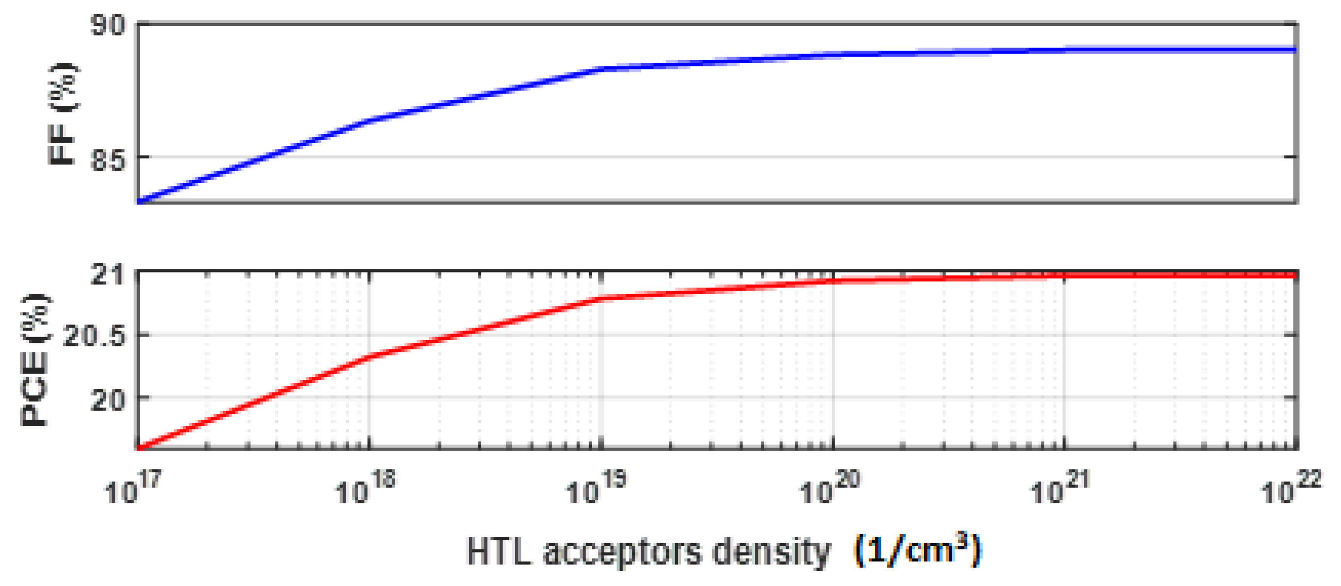
3.5.1. Effect of Acceptor Density of HTL

The doping of ETL and HTL can be carried out using one of two methods. Minority carriers can accomplish this, but this method dramatically reduces the photovoltaic characteristics. On the other hand, the majority of carriers with greatly improved PV characteristics can be achieved. A medium amount of doping density will assist in improving PSC performance. To get this optimum acceptor density, we have carried out device simulations for varying acceptor densities ranging from 1017 to 1022 cm−3. Lowering the acceptor density causes a rise in series resistance lowering the shunt resistance. As a result, the solar cell performance decreases [48]. Figure 6 depicts the influence of the acceptor density of HTL on PSCs’ performance characteristics from where the change in Jsc and Voc is not significant, and a slight linear increase can happen in the case of Jsc. FF and PCE curves rise from 83.3 to 89.03% and 19.6 to 20.96%, respectively. When the NA is higher, the electric interface field between the PSC layers grows, increasing electric potential. This improves the PCE of the PSC and strengthens the separation of the charge carriers with a slower recombination speed [49]. Furthermore, 1022 cm−3 is considered the optimum value of acceptor density as the best performance is achieved for this density which can be seen from the figure; further increase in acceptor density may cause a lowering of the hole mobility due to generating deep coulomb trappings [45].

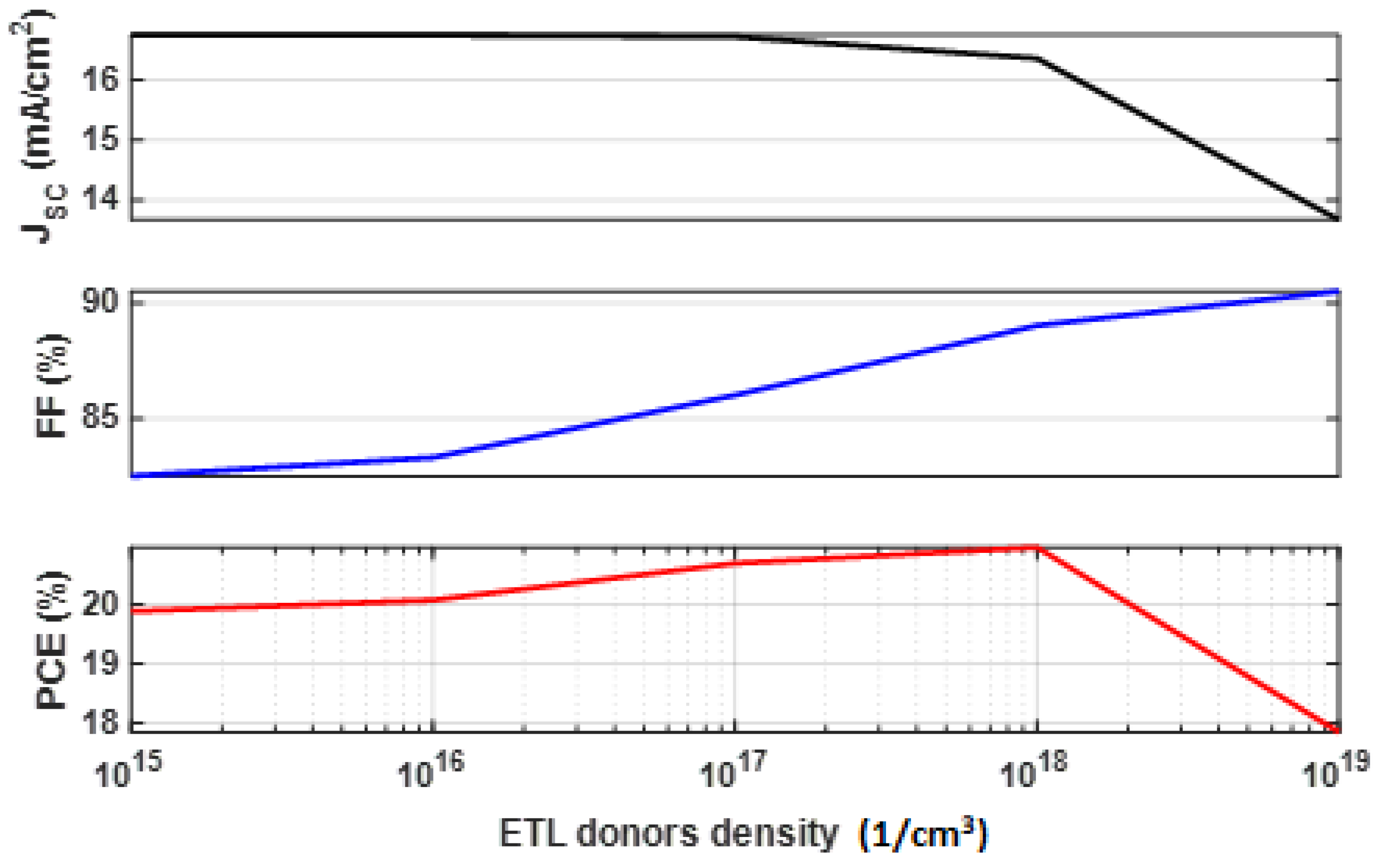
3.5.2. Effect of Acceptor Density of ETL

Figure 7 shows the impact of donor density of ETL on PSCs’ characteristics. To achieve a better performance, we have taken the previously optimized parameters from the preceding sections and varied the ND from 1015 to 1019 cm−3 to obtain the optimum donor density. It can be deduced from Figure 7 that the Jsc remained unchanged throughout the variation of ND (1015 to 1018 cm−3), and a sudden drop in Jsc takes place for further rising ND from 1018 to 1019 cm−3. The change in Voc is also too low to ignore due to variation in ND (from 1015 to 1018 cm−3), and a narrow increase occurs in Voc (1.4388 to 1.4425 V) due to further increase in ND (1018 to 1019 cm−3). After a gradual increase, a sudden drop can be seen from the figure in the case of PCE (20.96 to 17.84%) with increasing ND (1018 to 1019 cm−3). A constant rise in fill factor (82.53 to 90.51%) with rising ND is also observed.

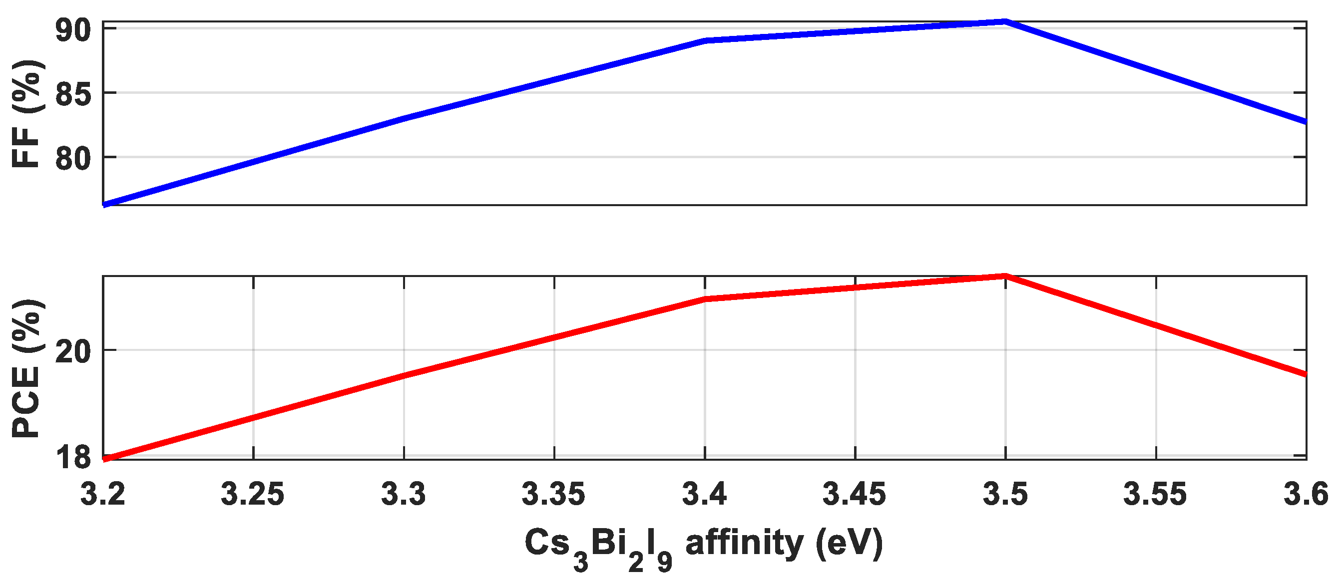
3.6. Effect of the Electron Affinity of the Absorber Layer

The electron affinity of a molecule is the amount of energy required to transform a neutral atom into a negative ion. The performance of the device can be largely affected by the electron affinity of the perovskite material, which is a crucial performance influencer parameter [50]. To realize the impact of the electron affinity of Cs3Bi2I9 on PSC’s performance characteristics, we have simulated the device configuration with various electron affinities of Cs3Bi2I9 ranging from 3.2 to 3.6 eV. The changes in characteristic curves can be seen in Figure 8, from where electron affinity is more impactful on PCE and FF. The short circuit current remains approximately similar for electron affinity 3.2 to 3.5 eV, and a slight drop occurs for a further rise (16.365 to 16.325 mA/cm2) in electron affinity (3.5 to 3.6 eV). A gradual increase in Voc can happen due to an increase in electron affinity. Furthermore, a linear increase in FF (76.25 to 90.53%) and PCE (17.92 to 21.4%) has occurred due to a rise in electron affinity from 3.2 to 3.5 eV. For further increases in electron affinity (3.5 to 3.6 eV), FF and PCE curves drop from 90.53 to 82.72% and 21.4 to 19.53%, respectively. Optimization of the electron affinity of the absorber layer is a critical task to obtain a good performance of PSCs. The best performance is achieved at the most suitable affinity of the absorber layer according to the ETL and the HTL affinities.

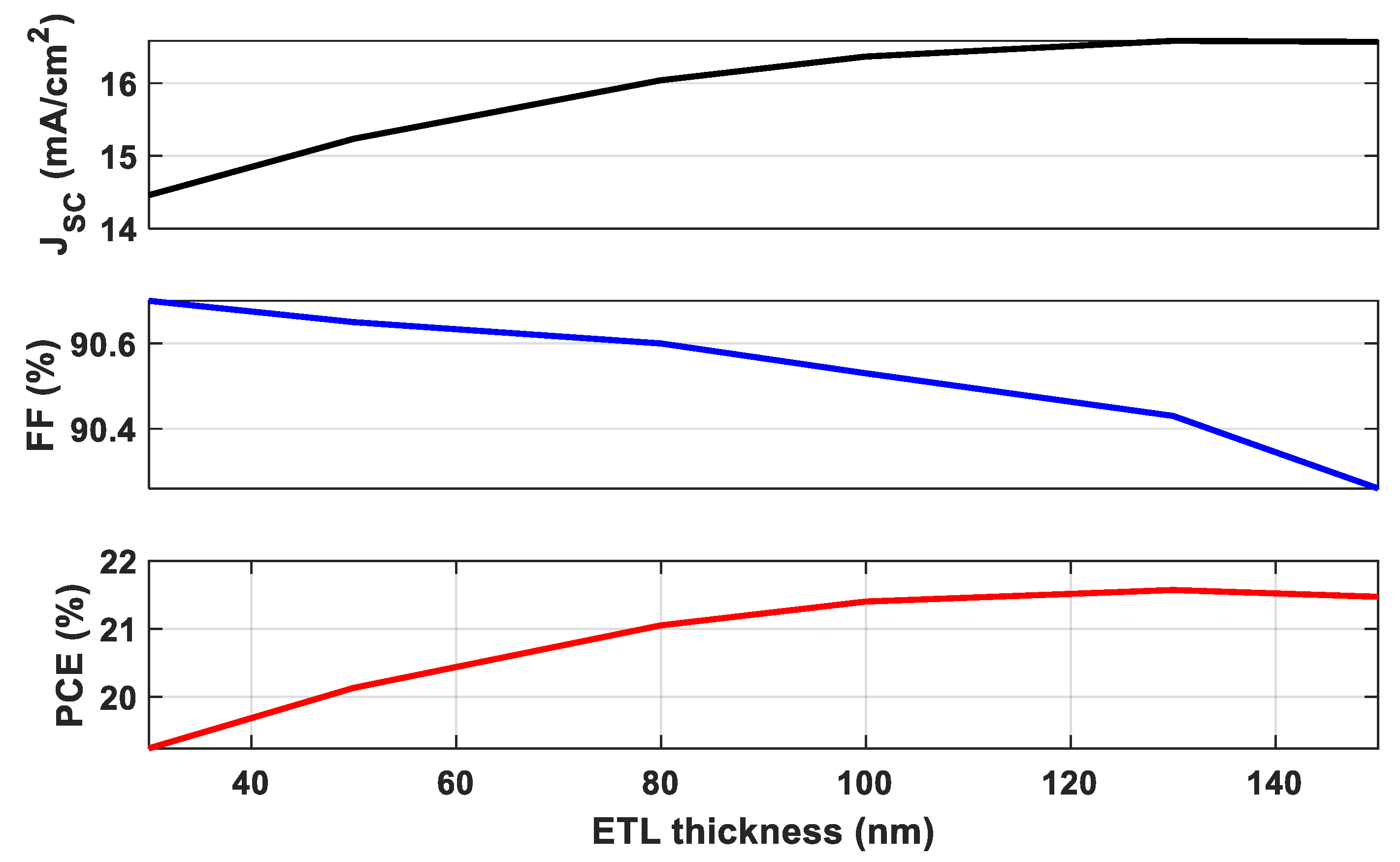
3.7. Effect of ETL Thickness

The thickness of the ETL plays an important role in device performance. ETL not only generates ways to move an electron from the AL but also works as a separator between the absorber layer and electrode [31]. Higher thickness of ETL may cause increased series resistance due to which recombination may occur, making the anode and cathode electrodes more difficult for charge ions (holes and electrons) to approach [51]. However, if the thickness of the ETL is reduced too much (below 50 nm), it becomes too thin to guarantee an adequate separation between the electrode and the absorber. To study the impact of variation of ETL thickness on device performance, we have carried out device simulations on varying ETL thickness from 30 to 150 nm. A gradual rise in Jsc and PCE curves and a gradual decline in FF are observed in Figure 9. Increasing ETL thickness from 30 to 150 nm, Jsc and PCE rise from 14.458 to 16.568 mA/cm2 and 19.24 to 21.47%, respectively. Voc and FF values decreased from 1.4668 to 1.4354 V and 90.7 to 90.26%, respectively. The maximum Jsc and PCE were obtained for 150 nm thickness of WS2.

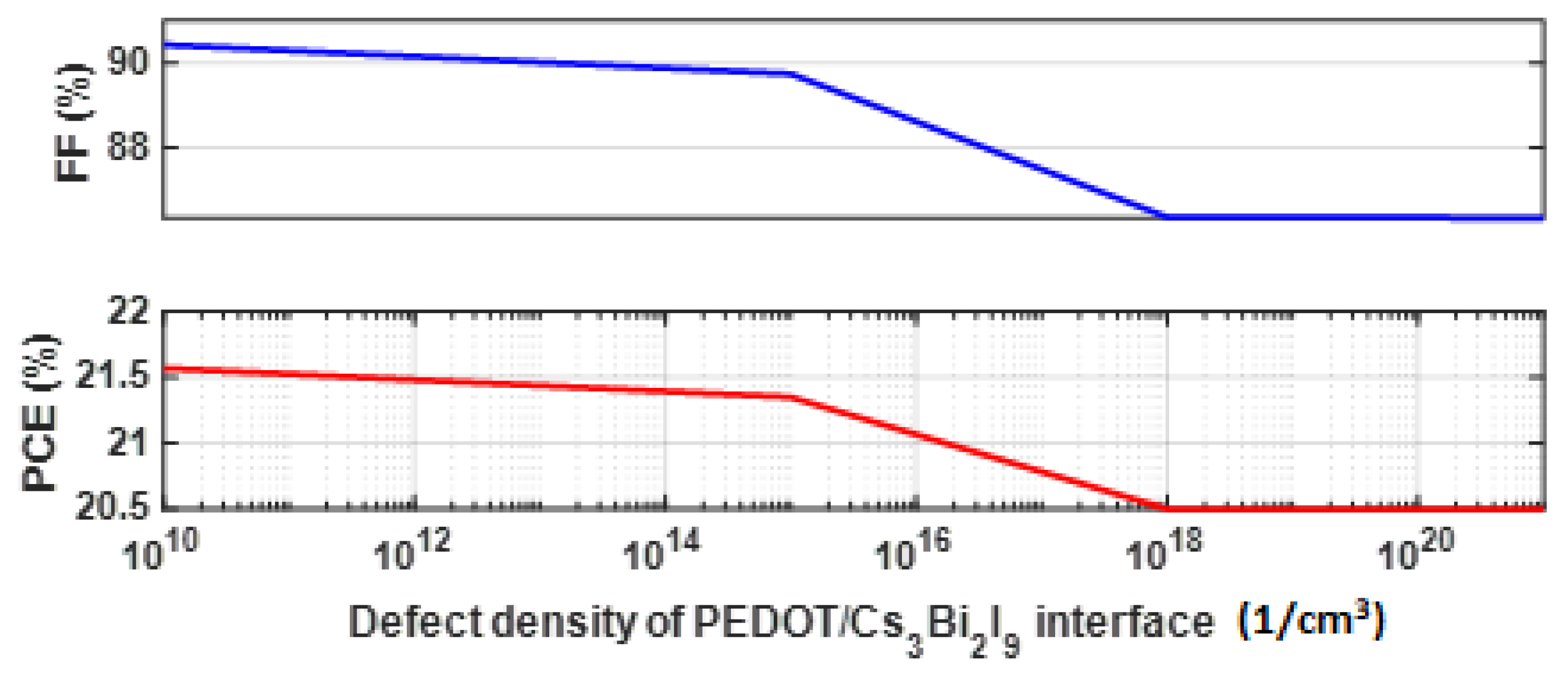
3.8. Effect of Defect Density of HTL/Absorber Interface

Structural mismatches between two materials or the introduction of environmental contaminants induce interfacial defects (i.e., charge recombination centers) to form in PSCs [52]. In the context of third-generation solar cells, the influence of the processing method is also critical (especially from solution). Additionally, non-radiative losses happen because of defects in the perovskite absorber and poor electrical quality in the heterojunctions between the perovskite/charge extraction layer (HTL or ETL), which results in the Voc loss [53]. The performance and long-term stability of the device are also impacted by the interfaces of the several PSC layers. Trap-assisted non-radiative recombination results in voltage and current loss when an interface with several defects/voids or trap states is used. To understand the effect of HTL/absorber layer interface defect density, we have taken this value ranging from 1010 to 1021 cm−3. The impact of the defect density of the HTL/AL interface on PSC performance is much slighter. From Figure 10, these effects can be seen for various performance parameters. Due to an increase in defect density from 1010 to 1018 cm−3, a gradual decrease in performance parameters can be observed. These parameters remain unchanged due to further variation in interface defect density (1018 to 1021 cm−3).

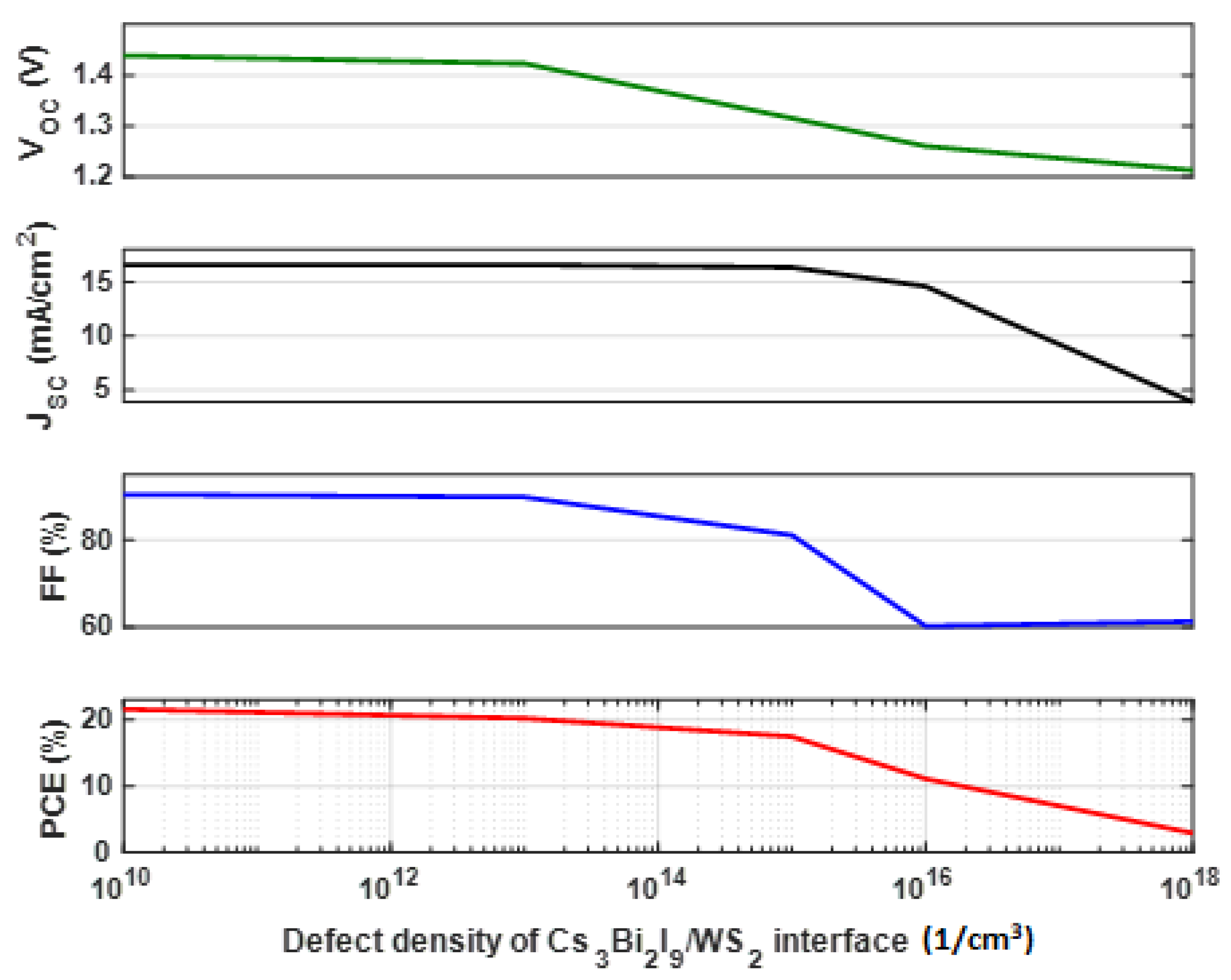
3.9. Effect of Defect Density of ETL/Absorber Interface

The performance of a PSC device is greatly influenced by front interface defects rather than rear interface defects. This phenomenon can be explained by the high absorption coefficient of perovskite materials, which causes more photon absorption near the front contact. As a result, several electron-hole pairs are generated close to the front contact. Now, the ratio of charge carriers to trap-assisted recombination is known. As a result, we see that issues with the front interface have a worse impact on the functionality of the device. Consequently, we must pay attention to defect passivation at the front interface. Several technologies have been developed to passivate the interface defects, such as ionic liquid engineering [54], antisolvent treatment [55], and the application of graphene-based, fullerene-based, and alkali salt-based modifiers [56].
The influence of HTL/absorber layer interface defect density on PSC performance parameters can be realized in Figure 11, where a gradual decline in Voc (1.4388 to 1.2133 V) can be observed due to an increase in interface defect density (1010 to 1018cm−3). In contrast, the change in Jsc is not much bigger in the first four steps of interface defect density variation (1010 to 1016 cm−3), but a huge drop in Jsc (14.594 to 3.897 mA/cm2) occurs due to a further increase in defect density (1016 to 1018 cm−3). Furthermore, a gradual decline is also observed in FF and PCE due to increasing WS2/Cs3Bi2I9 interface defect density, where FF decreased from 90.43 to 61.34% and PCE reduced from 21.57 to 2.9%, respectively.

3.10. Effect of Rs on Device Performance

The performance of the PSC device is significantly impacted by the series (Rs) resistance. This factor is one of the key elements in defining junction qualities and how they affect solar cell device performance. The series resistance generates from the front and rear contacts, interfaces, and bulk resistance that generates due to the movement of current.
By increasing Rs by 10 Ω/cm2, the PCE falls from 21.31% to 18.96%. Due to a further increase in Rs from 10 to 100 Ω/cm2, a huge drop in PCE from 18.96% to 5.06% occurs, and the fill factor also decreases from 79.45% to 25.3%. Therefore, to obtain high efficiency, the series resistance should be minimum.
P l o s s = J s c 2 R s ,
From Equation (8), it can be explained how power loss increases with the rising series resistance. The resistance on interfaces and front/rear contacts can be improved using a suitable manufacturing process and applying interface modifiers [57,58]. Furthermore, bulk resistance can be minimized by applying appropriate chemical compounds in the ETL and HTL [59].

3.11. Effect of Rsh on Device Performance

The shunt resistance is a critical parameter that highly affects the performance parameters of perovskite solar cells. Different charge recombination ways may cause an increase in shunt resistance [60]. Previously tuned performance influencers were considered to understand the impact of shunt resistance (Rsh) on PSC characteristics. To understand the effect of shunt resistance, we varied the value of Rsh from 102 to 105.
The open circuit voltage rose when the Rsh varied from 100 to 1000 Ω/cm2, and for further increase in Rsh, the Voc remains unchanged. A high rise in FF (29.78% to 83.09%) and PCE (6.85% to 19.78%) occurs when the Rsh increases from 100 to 1000 Ω/cm2. For further increase in Rsh, the fill factor and PCE increases slightly. It can be clarified that high shunt resistance is necessary to maximize the performance of PSCs. Previously published articles also have reported the same behavior [61]. Alternative current passing ways generated due to charge carriers are the key factors for lowering the shunt resistance. Usually, poor design of PSC devices and fabrication errors cause major impacts on the shunt resistance of a solar cell device. The shunt resistance decreases due to the application of back contact materials with a low work function that will cause a reduction in the PCE of the solar cell device.

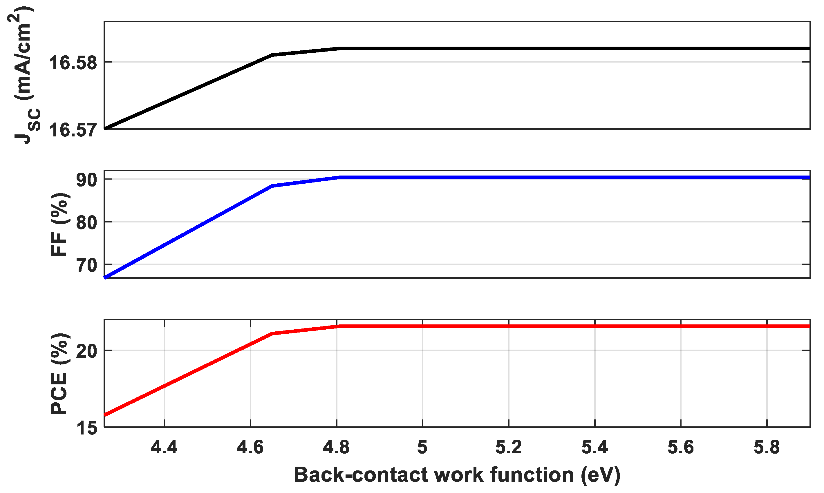
3.12. Effect of the Work Function of Rear Contact Material

The metal contacts’ main function is to enable the transformation of solar cell electricity to an external circuit [62]. There are a variety of rear contact metals available with various work function values. Au and Ag are two rear-contact metals that are frequently employed in PSCs. However, they have significant disadvantages because of their instability or expensive processing. Therefore, choosing an appropriate back-contact material with an optimal work function is required to achieve the best device performance parameters. Various metals, including Ag, Cu, Fe, Au, and Pd, with work functions of 4.26, 4.65, 4.81, 5.1, and 5.9 eV, respectively, are used as rear contacts to improve the performance of the modeled devices under study. When using back contacts with high work function, the device’s performance is steady and has a high PCE which can be observed in Figure 12. On the other hand, the use of Ag as back material gives a poor performance of the simulated PSC device because the flat band condition cannot be achieved.

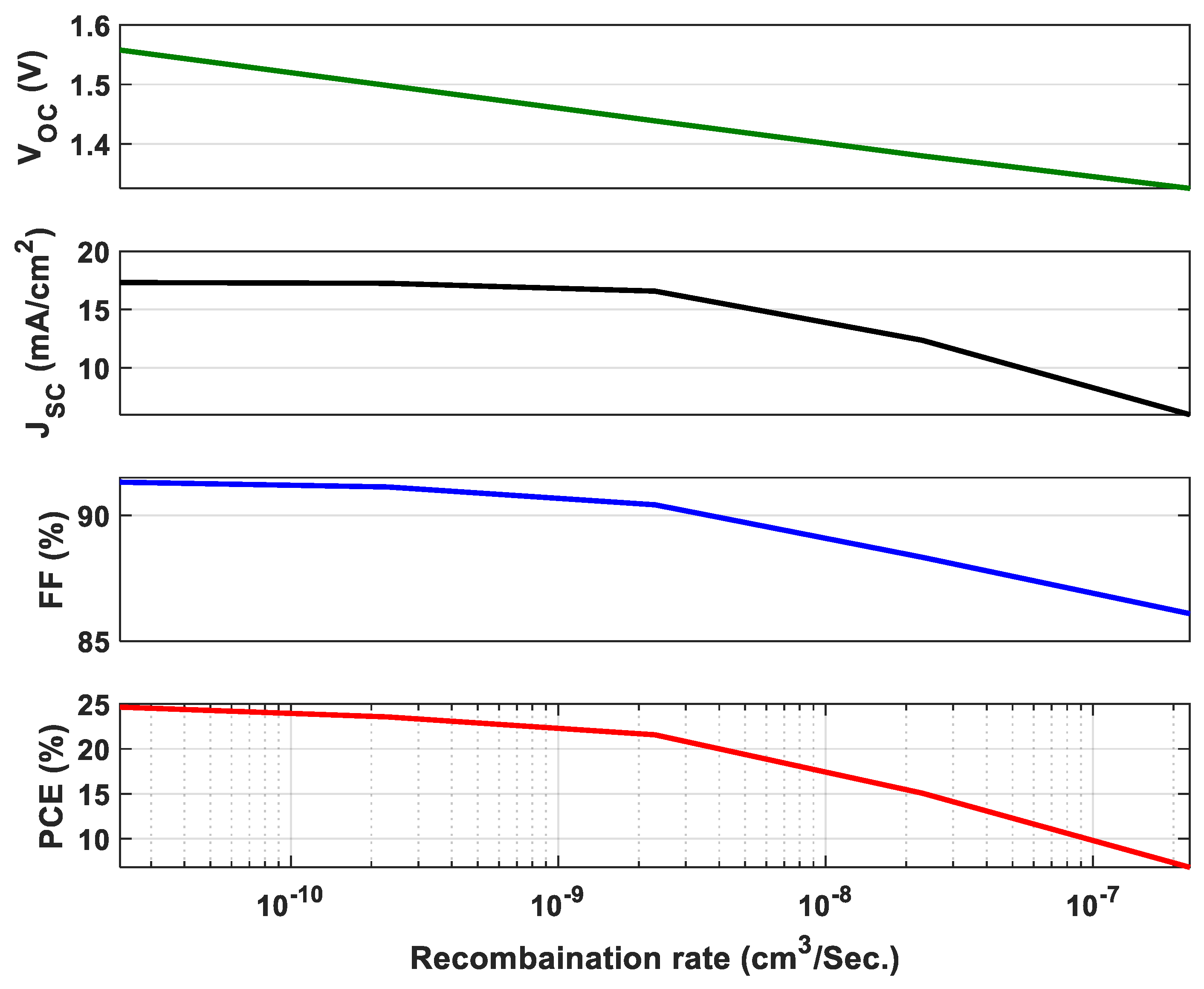
3.13. Effect of Band-to-Band Radiative Recombination Rate

The most common recombination rate for PSC devices is the radiative recombination rate between the conduction and valence band. It is adjusted in this section to investigate and evaluate the impact on the PSC characteristics. In solar cell system science, band-to-band (Radiative), Shockley–Read–Hall (SRH), and Auger recombination approaches are typically explored [63]. Only at higher penetration levels does the Auger process seem relevant. In contrast, SRH is influenced by defect states and densities and is closely related to the methods used in the processing of materials, the deposition of materials, and the manufacturing of devices. An electron enters the conduction band when a photon is trapped in the perovskite layer, but this is a non-equilibrium process. The term “band-to-band (Radiative) recombination” is used to describe this. The carrier density of states in the perovskite layer controls radiative recombination. To better understand how it affects device performance, we changed the rate of recombination rate from 2.3 × 10 −7 cm3/s to 2.3 × 10⁻¹¹ cm3/s. In Figure 13, it can be deduced that a linear decrease occurs in Voc (1.3252 to 1.5579 V) due to the increase in recombination rate, and a great decrease occurs in Jsc (17.32 to 5.975 mA/cm2). The effect of the recombination rate is much higher on PCE. The PCE decreases from 24.65 to 6.82% due to increasing the recombination rate from 2.3 × 10⁻⁷ to 2.3 × 10⁻¹¹ cm3/s, as illustrated in Figure 13. Along with increasing the recombination rate, the fill factor decreases as well. In contrast, the PSC performance degrades as radiative recombination rises.

3.14. Effect of Operating Temperature on Device Performance

The general operating temperature used during simulation in the current investigation was 300 K. However, the temperature of PSCs can be changed during manufacture, characterization, and outside use. The operating temperature is affected by height, latitude, the time of day in a certain location, and the season. The operating temperature affects how well a PSC device performs.
A decrease in the Voc is the main factor that primarily causes the PCE to decrease as the temperature rises. It has been found that when the temperature rises, Voc decreases. Equation (9) shows how the open circuit voltage changes as a function of temperature.
d V o c d T = V o c T + K T q 1 J s c d J s c d T 1 J 0 d J 0 d T ,
It is clear from Equation (9) that short circuit current and reverse saturation current (J0) impact how Voc varies with temperature. The voltage drops as the temperature rises because the J0 rises. With an increase in temperature, JSC is found to increase by a tiny amount. However, the magnitude increment is insufficient to maintain the solar cell’s overall performance. The slight increase in JSC causes bandgap’s narrowing with rising temperature. Equation (10) illustrates how temperature affects bandgap at a specific temperature where α and β are constants, and these are the bandgaps of semiconductors at 0 K and temperature T, respectively.
E g T = E g 0 α T 2 T + β ,
The decrease in the FF is also seen as the temperature rises. The relationship between FF and temperature (T) can be shown by Equation (11).
d F F d T = d V o c d T V o c T V o c + K T q V o c q K T 0.28 V o c q K T + 0.72 ,
As the operating temperature rises from 300 K to 400 K, there is a decrease in PCE value. Although the PSCs’ performance with temperature increases and their thermal stability can be precisely studied experimentally, we analyzed the behavior theoretically to acquire a basic view. More research on the performance of PSCs with temperature change can be viewed in previous reports [64,65].

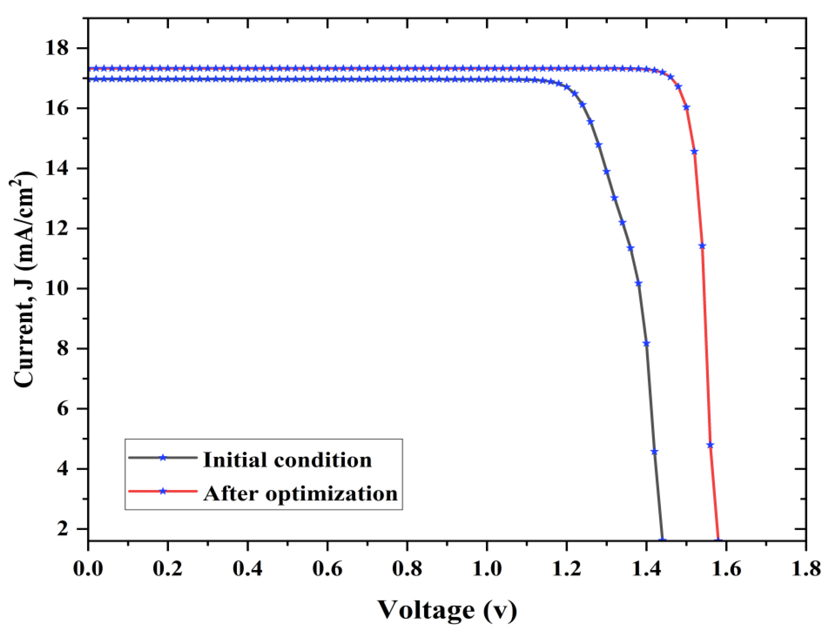
3.15. The Optimized Configuration

In this study, we have simulated seven novel models with seven HTL materials from these models. The best configuration was ITO/WS2/Cs3Bi2I9/PEDOT:PSS/Au, for which we achieved the best performance parameters. For further improvement, this model was optimized by varying parameters such as thickness, bandgap, defect density, the electron affinity of the absorber layer, charge carrier density, temperature, series and shunt resistance, work function, etc. Figure 14 shows the comparison of J-V curves of the initial and final PSCs. After optimizing this novel model, we achieved 24.91% of PCE, 91.66% FF, 17.325 mA/cm2 of Jsc, and 1.5683V of Voc.

4. Challenges and Conclusions

Though perovskite-based solar cells achieve high efficiencies, the main barriers observed in perovskite solar cells are toxicity and stability. Toxicity can be eliminated from the solar cell industries by avoiding using lead-based perovskite materials. In this study, a lead-free perovskite layer Cs3Bi2I9 was selected that is free from any toxicity. The factors that cause instability and novel stabilization procedures developed to be used industrially are discussed. The stability of perovskite solar cells can be classified as intrinsic and extrinsic. Intrinsic stability includes—electronic band structure and stability against defects, structural stability, and thermodynamic phase stability. In contrast, extrinsic stability includes moisture stability, thermochemical stability, light stability, device thermal stability, stability against electrode degradation, oxidation, and photooxidation stabilities. Researchers have established different technologies to improve the stability of PSC devices with increased efficiencies. Among these technologies, additive, solvent, and composition engineering have caught great attention in industries.

4.1. Additive Engineering

This method has gained a lot of popularity, especially in producing PSCs on a big scale. It has been observed that the application of additives results in consistent morphology, improved stability, and a greater decrease in defect density. Morphological control becomes crucial to prevent shunt routes, ensure excellent absorption, and ensure the homogeneous production of ETL and HTL layers. By modifying the solution dynamics, such as temperature, supersaturation, and substrate wettability, the additives enable us to regulate growth and nucleation. The additives may engage in interactions with the substrate, the solvent, or the solute. Many additions have been investigated for improved morphology [66].

4.2. Composition Engineering

This is an established process for enhancing PSC devices’ efficiency and stability. It is a proven effective method for increasing PCE. In this method, one material of the composition of fabricated perovskite is changed with a new material; thus, a new composition can be achieved with higher efficiency and stability [67].

4.3. Solvent Engineering

To decrease the GB surface area, solvent engineering techniques have been widely used to increase the average grain size and crystallinity of the perovskite polycrystalline film [68]. Because of the uneven distribution of the anti-solvent, solvent engineering for PSCs has improved control over manufacturing at the lab scale but is still unsuitable for large-scale use [69].

4.4. Stability Induced by Charge Carrier Layers

Charge transporting layers such as ETL and HTL play a key role in achieving high efficiency and stability in PSCs. In this case, the energy band structure of the charge carrier layer is more crucial as a well-matched layer facilitates the movements of charges in respective electrodes. Charge separation is also improved, which can reduce the recombination rate [70]. Moreover, less energy will be loosed when easy transportation of charges occurs due to selecting appropriate charge transporting layers.

4.5. Conclusions

A novel efficient Cs3Bi2I9-based perovskite-based solar cell configuration is proposed in this study, with a full analysis showing an energy conversion PCE of 24.91%. The results were reached using a step-by-step method that included numerical analysis of a configuration with well-suited layers. SCAPS-1D software was used to model the device and to simulate the configuration varying several variables such as thickness, bandgap, defect density, carrier density, etc., to investigate the optimum performance parameters. Numerical simulation was carried out for different PSC configurations with seven hole transport layers, among which ITO/WS2/Cs3Bi2I9/PEDOT:PSS/Au shows the best performance. After improving this configuration through scrutinized optimization, its performance parameters were found as Jsc of 17.325 mA/cm2, Voc of 1.5683V, FF of 91.66%, and PCE of 24.91%. This study contributes to a better knowledge of the performance of Cs3Bi2I9-based PSCs and guides the modeling of the efficient device topology. The concepts and criteria offered in this study can be useful in projecting possible manufacturing processes for cost-effective and efficient perovskite solar cells. The world is experiencing an energy shift into renewables. Therefore, the opportunity to manufacture an energy system having high efficiency and a cost-effective solution is enormous. While the present study investigates a lead-free inorganic perovskite solar system capable of promoting sustainable socio-environmental development, further research is warranted to investigate the performance parameters experimentally.

Author Contributions

Conceptualization, A.D., S.D.P., M.A.M.A. and B.K.D.; methodology, A.D., S.D.P., M.A.M.A., B.K.D. and M.S.H.; validation and formal analysis, A.D., S.D.P., M.A.M.A., B.K.D. and M.S.H.; resources, A.D., S.D.P. and M.M.S.; data curation, A.D., S.D.P. and M.M.S.; visualization, A.D., S.D.P., M.M.S. and M.A.M.A.; investigation, all authors; writing—original draft preparation, A.D., S.D.P., M.A.M.A. and M.S.H.; writing—review and editing, A.D., B.K.D. and M.M.S.; supervision, B.K.D. and M.M.S. All authors have read and agreed to the published version of the manuscript.

Funding

This research received no external funding.

Data Availability Statement

No new data were created or analyzed in this study. Data sharing does not apply to this article.

Conflicts of Interest

The authors declare no conflict of interest.

References

  1. Akanda, A.M.; Shin, D. A synthesis parameter of molten salt nanofluids for solar thermal energy storage applications. J. Energy Storage 2023, 60, 106608. [Google Scholar] [CrossRef]
  2. Das, A.; Peu, S.D.; Akanda, M.A.M.; Islam, A.R.M.T. Peer-to-Peer Energy Trading Pricing Mechanisms: Towards a Comprehensive Analysis of Energy and Network Service Pricing (NSP) Mechanisms to Get Sustainable Enviro-Economical Energy Sector. Energies 2023, 16, 2198. [Google Scholar] [CrossRef]
  3. Doğan, B.; Ghosh, S.; Shahzadi, I.; Balsalobre-Lorente, D.; Nguyen, C.P. The relevance of economic complexity and economic globalization as determinants of energy demand for different stages of development. Renew. Energy 2022, 190, 371–384. [Google Scholar] [CrossRef]
  4. Das, A.; Peu, S.D. A Comprehensive Review on Recent Advancements in Thermochemical Processes for Clean Hydrogen Production to Decarbonize the Energy Sector. Sustainability 2022, 14, 11206. [Google Scholar] [CrossRef]
  5. Mehadi, H.; Fatema, T.Z.; Saleha, A. A Review on Energy Situation ‘Solar Energy Policies and Targets’ in SAARC Countries. J. Energy Nat. Resour 2017, 6, 45–51. [Google Scholar]
  6. Sahare, S.; Pham, H.D.; Angmo, D.; Ghoderao, P.; MacLeod, J.; Khan, S.B.; Lee, S.; Singh, S.P.; Sonar, P. Emerging Perovskite Solar Cell Technology: Remedial Actions for the Foremost Challenges. Adv. Energy Mater. 2021, 11, 2101085. [Google Scholar] [CrossRef]
  7. Dai, X.; Chen, S.; Jiao, H.; Zhao, L.; Wang, K.; Ni, Z.; Yu, Z.; Chen, B.; Gao, Y.; Huang, J. Efficient monolithic all-perovskite tandem solar modules with small cell-to-module derate. Nat. Energy 2022, 7, 923–931. [Google Scholar] [CrossRef]
  8. Green, M.A.; Ho-Baillie, A.; Snaith, H.J. The emergence of perovskite solar cells. Nat. Photonics 2014, 8, 506–514. [Google Scholar] [CrossRef]
  9. Lee, Y.H.; Luo, J.; Son, M.-K.; Gao, P.; Cho, K.T.; Seo, J.; Zakeeruddin, S.M.; Grätzel, M.; Nazeeruddin, M.K. Enhanced Charge Collection with Passivation Layers in Perovskite Solar Cells. Adv. Mater. 2016, 28, 3966–3972. [Google Scholar] [CrossRef]
  10. Kojima, A.; Teshima, K.; Shirai, Y.; Miyasaka, T. Organometal halide perovskites as visible-light sensitizers for photo-voltaic cells. J. Am. Chem. Soc. 2009, 131, 6050–6051. [Google Scholar] [CrossRef]
  11. Zhu, Y.; Liu, Y.; Miller, K.A.; Zhu, H.; Egap, E. Lead Halide Perovskite Nanocrystals as Photocatalysts for PET-RAFT Polymerization under Visible and Near-Infrared Irradiation. ACS Macro Lett. 2020, 9, 725–730. [Google Scholar] [CrossRef] [PubMed]
  12. Xu, Y.F.; Yang, M.Z.; Chen, B.X.; Wang, X.D.; Chen, H.Y.; Kuang, D.B.; Su, C.Y. A CsPbBr3 Perovskite Quantum Dot/Graphene Oxide Composite for Photocatalytic CO2 Reduction. J. Am. Chem. Soc. 2017, 139, 5660–5663. [Google Scholar] [CrossRef] [PubMed]
  13. Zhu, Y.; Liu, Y.; Ai, Q.; Gao, G.; Yuan, L.; Fang, Q.; Tian, X.; Zhang, X.; Egap, E.; Ajayan, P.M.; et al. In Situ Synthesis of Lead-Free Halide Perovskite–COF Nanocomposites as Photocatalysts for Photoinduced Polymerization in Both Organic and Aqueous Phases. ACS Mater. Lett. 2022, 4, 464–471. [Google Scholar] [CrossRef]
  14. Jošt, M.; Kegelmann, L.; Korte, L.; Albrecht, S. Monolithic Perovskite Tandem Solar Cells: A Review of the Present Status and Advanced Characterization Methods Toward 30% Efficiency. Adv. Energy Mater. 2020, 10, 1904102. [Google Scholar] [CrossRef]
  15. Li, Q.; Zhao, Y.; Zhou, W.; Han, Z.; Fu, R.; Lin, F.; Yu, D.; Zhao, Q. Halogen Engineering for Operationally Stable Perovskite Solar Cells via Sequential Deposition. Adv. Energy Mater. 2019, 9, 1902239. [Google Scholar] [CrossRef]
  16. Hu, Y.; Qiu, T.; Bai, F.; Ruan, W.; Zhang, S. Highly Efficient and Stable Solar Cells with 2D MA3 Bi2 I9 /3D MAPbI3 Heterostructured Perovskites. Adv. Energy Mater. 2018, 8, 1703620. [Google Scholar] [CrossRef]
  17. Ghosh, B.; Wu, B.; Mulmudi, H.K.; Guet, C.; Weber, K.; Sum, T.C.; Mhaisalkar, S.; Mathews, N. Limitations of Cs3Bi2I9 as Lead-Free Photovoltaic Absorber Materials. ACS Appl. Mater. Interfaces 2018, 10, 35000–35007. [Google Scholar] [CrossRef]
  18. Xiao, Z.; Meng, W.; Wang, J.; Mitzi, D.B.; Yan, Y. Searching for promising new perovskite-based photovoltaic absorbers: The importance of electronic dimensionality. Mater. Horizons 2017, 4, 206–216. [Google Scholar] [CrossRef]
  19. Morgan, A.B.; Putthanarat, S. Use of inorganic materials to enhance thermal stability and flammability behavior of a polyimide. Polym. Degrad. Stab. 2011, 96, 23–32. [Google Scholar] [CrossRef]
  20. Koh, T.M.; Krishnamoorthy, T.; Yantara, N.; Shi, C.; Leong, W.L.; Boix, P.P.; Grimsdale, A.C.; Mhaisalkar, S.G.; Mathews, N. Formamidinium tin-based perovskite with low Eg for photovoltaic applications. J. Mater. Chem. A 2015, 3, 14996–15000. [Google Scholar] [CrossRef]
  21. Chen, X.; Jia, M.; Xu, W.; Pan, G.; Zhu, J.; Tian, Y.; Wu, D.; Li, X.; Shi, Z. Recent Progress and Challenges of Bismuth-Based Halide Perovskites for Emerging Optoelectronic Applications. Adv. Opt. Mater. 2022, 11, 2202153. [Google Scholar] [CrossRef]
  22. Jayan, D.J. Bandgap Tuning and Input Parameter Optimization for Lead-Free All-Inorganic Single, Double, and Ternary Perovskite-Based Solar Cells. Sol. RRL 2021, 6, 2100971. [Google Scholar] [CrossRef]
  23. Burgelman, M.; Nollet, P.; Degrave, S. Modelling polycrystalline semiconductor solar cells. Thin Solid Film. 2000, 361–362, 527–532. [Google Scholar] [CrossRef]
  24. Ghosh, B.; Chakraborty, S.; Wei, H.; Guet, C.; Li, S.; Mhaisalkar, S.; Mathews, N. Poor Photovoltaic Performance of Cs3Bi2I9: An Insight through First-Principles Calculations. J. Phys. Chem. C 2017, 121, 17062–17067. [Google Scholar] [CrossRef]
  25. Islam, A.; Islam, S.; Sobayel, K.; Emon, E.; Jhuma, F.; Shahiduzzaman, M.; Akhtaruzzaman, M.; Amin, N.; Rashid, M. Performance analysis of tungsten disulfide (WS2) as an alternative buffer layer for CdTe solar cell through numerical modeling. Opt. Mater. 2021, 120, 111296. [Google Scholar] [CrossRef]
  26. Sobayel, K.; Akhtaruzzaman, M.; Rahman, K.; Ferdaous, M.; Al-Mutairi, Z.A.; Alharbi, H.F.; Alharthi, N.H.; Karim, M.R.; Hasmady, S.; Amin, N. A comprehensive defect study of tungsten disulfide (WS2) as electron transport layer in perovskite solar cells by numerical simulation. Results Phys. 2019, 12, 1097–1103. [Google Scholar] [CrossRef]
  27. Islam, T.; Jani, R.; Shorowordi, K.M.; Hoque, Z.; Gokcek, A.M.; Vattipally, V.; Nishat, S.S.; Ahmed, S. Numerical simulation studies of Cs3Bi2I9 perovskite solar device with optimal selection of electron and hole transport layers. Optik 2021, 231, 166417. [Google Scholar] [CrossRef]
  28. Zuo, C.; Ding, L. Solution-Processed Cu2O and CuO as Hole Transport Materials for Efficient Perovskite Solar Cells. Small 2015, 11, 5528–5532. [Google Scholar] [CrossRef]
  29. Mousa, M.; Salah, M.M.; Zekry, A.; Abouelatta, M.; Shaker, A.; Amer, F.Z.; Mubarak, R.I.; Saeed, A. Simulation of High open-circuit voltage Perovskite/CIGS-GeTe tandem cell. In Proceedings of the 2022 IEEE 49th Photovoltaics Specialists Conference (PVSC), Philadelphia, PA, USA, 5–10 June 2022; pp. 1230–1234. [Google Scholar] [CrossRef]
  30. Kumar, M.H.; Dharani, S.; Leong, W.L.; Boix, P.P.; Prabhakar, R.R.; Baikie, T.; Shi, C.; Ding, H.; Ramesh, R.; Asta, M.; et al. Lead-Free Halide Perovskite Solar Cells with High Photocurrents Realized Through Vacancy Modulation. Adv. Mater. 2014, 26, 7122–7127. [Google Scholar] [CrossRef]
  31. Raoui, Y.; Ez-Zahraouy, H.; Tahiri, N.; El Bounagui, O.; Ahmad, S.; Kazim, S. Performance analysis of MAPbI3 based perovskite solar cells employing diverse charge selective contacts: Simulation study. Sol. Energy 2019, 193, 948–955. [Google Scholar] [CrossRef]
  32. Chen, D.; Wang, Y.; Lin, Z.; Huang, J.; Chen, X.; Pan, D.; Huang, F. Growth Strategy and Physical Properties of the High Mobility P-Type CuI Crystal. Cryst. Growth Des. 2010, 10, 2057–2060. [Google Scholar] [CrossRef]
  33. Hodes, G. Perovskite-Based Solar Cells. Science 2013, 342, 317–318. [Google Scholar] [CrossRef] [PubMed]
  34. Liu, D.; Gangishetty, M.K.; Kelly, T.L. Effect of CH3NH3PbI3thickness on device efficiency in planar heterojunction perovskite solar cells. J. Mater. Chem. A 2014, 2, 19873–19881. [Google Scholar] [CrossRef] [Green Version]
  35. Wu, H.; Wang, L.-S. A study of nickel monoxide (NiO), nickel dioxide (ONiO), and Ni(O2) complex by anion photoelectron spectroscopy. J. Chem. Phys. 1997, 107, 16–21. [Google Scholar] [CrossRef] [Green Version]
  36. Salah, M.M.; Hassan, K.M.; Abouelatta, M.; Shaker, A. A comparative study of different ETMs in perovskite solar cell with inorganic copper iodide as HTM. Optik 2018, 178, 958–963. [Google Scholar] [CrossRef]
  37. Hock, R.; Mayer, T.; Jaegermann, W. P-type doping of spiro-MeOTAD with WO 3 and the spiro-MeOTAD/WO 3 interface investigated by synchrotron-induced photoelectron spectroscopy. J. Phys. Chem. C 2012, 116, 18146–18154. [Google Scholar] [CrossRef]
  38. Salah, M.M.; Zekry, A.; Shaker, A.; Abouelatta, M.; Mousa, M.; Saeed, A. Investigation of Electron Transport Material-Free Perovskite/CIGS Tandem Solar Cell. Energies 2022, 15, 6326. [Google Scholar] [CrossRef]
  39. Du, H.-J.; Wang, W.-C.; Zhu, J.-Z. Device simulation of lead-free CH 3 NH 3 SnI 3 perovskite solar cells with high efficiency. Chin. Phys. B 2016, 25, 108802. [Google Scholar] [CrossRef]
  40. Anwar, F.; Mahbub, R.; Satter, S.S.; Ullah, S.M. Effect of Different HTM Layers and Electrical Parameters on ZnO Nanorod-Based Lead-Free Perovskite Solar Cell for High-Efficiency Performance. Int. J. Photoenergy 2017, 2017, 9846310. [Google Scholar] [CrossRef]
  41. Ameri, M.; Mohajerani, E.; Ghafarkani, M.; Safari, N.; Alavi, S.A. The investigation of the unseen interrelationship of grain size, ionic defects, device physics and performance of perovskite solar cells. J. Phys. D Appl. Phys. 2019, 52, 125501. [Google Scholar] [CrossRef]
  42. Kim, H.; Lim, K.-G.; Lee, T.-W. Planar heterojunction organometal halide perovskite solar cells: Roles of interfacial layers. Energy Environ. Sci. 2016, 9, 12–30. [Google Scholar] [CrossRef]
  43. Barbé, J.; Tietze, M.L.; Neophytou, M.; Murali, B.; Alarousu, E.; El Labban, A.; Abulikemu, M.; Yue, W.; Mohammed, O.F.; McCulloch, I.; et al. Amorphous Tin Oxide as a Low-Temperature-Processed Electron-Transport Layer for Organic and Hybrid Perovskite Solar Cells. ACS Appl. Mater. Interfaces 2017, 9, 11828–11836. [Google Scholar] [CrossRef] [PubMed]
  44. Park, H.; Khokhar, M.Q.; Cho, E.-C.; Ju, M.; Kim, Y.; Kim, S.; Yi, J. Computer modeling of the front surface field layer on the performance of the rear-emitter silicon heterojunction solar cell with 25% efficiency. Optik 2019, 205, 164011. [Google Scholar] [CrossRef]
  45. Salah, M.M.; Abouelatta, M.; Shaker, A.; Hassan, K.M.; Saeed, A. A comprehensive simulation study of hybrid halide perovskite solar cell with copper oxide as HTM. Semicond. Sci. Technol. 2019, 34, 115009. [Google Scholar] [CrossRef]
  46. Lee, Y.M.; Maeng, I.; Park, J.; Song, M.; Yun, J.H.; Jung, M.C.; Nakamura, M. Comprehensive Understanding and Controlling the Defect Structures: An Effective Approach for Organ-ic-Inorganic Hybrid Perovskite-Based Solar-Cell Application. Front. Energy Res. 2018, 6, 128. [Google Scholar] [CrossRef] [Green Version]
  47. Rai, S.; Pandey, B.; Dwivedi, D. Modeling of highly efficient and low cost CH3NH3Pb(I1-xClx)3 based perovskite solar cell by numerical simulation. Opt. Mater. 2019, 100, 109631. [Google Scholar] [CrossRef]
  48. Zhou, X.; Han, J. Design and simulation of C2N based solar cell by SCAPS-1D software. Mater. Res. Express 2020, 7, 126303. [Google Scholar] [CrossRef]
  49. Mohandes, A.; Moradi, M.; Nadgaran, H. Numerical simulation of inorganic Cs2AgBiBr6 as a lead-free perovskite using device simulation SCAPS-1D. Opt. Quantum Electron. 2021, 53, 319. [Google Scholar] [CrossRef]
  50. Jayan, K.D.; Sebastian, V. Comparative performance analysis of mixed halide perovskite solar cells with different transport layers and back metal contacts. Semicond. Sci. Technol. 2021, 36, 065010. [Google Scholar] [CrossRef]
  51. Hosseini, S.; Delibaş, N.; Bahramgour, M.; Mashayekh, A.T.; Niaie, A. Performance Comparison of Different Hole Transport Layer Configurations in a Perovskite-based Solar Cell using SCAPS-1D Simulation. Eur. J. Sci. Technol. 2021, 31, 121–126. [Google Scholar] [CrossRef]
  52. Basyoni, M.S.S.; Salah, M.M.; Mousa, M.; Shaker, A.; Zekry, A.; Abouelatta, M.; Alshammari, M.T.; Al-Dhlan, K.A.; Gontrand, C. On the Investigation of Interface Defects of Solar Cells: Lead-Based vs Lead-Free Perovskite. IEEE Access 2021, 9, 130221–130232. [Google Scholar] [CrossRef]
  53. Mahesh, S.; Ball, J.M.; Oliver, R.D.J.; McMeekin, D.P.; Nayak, P.K.; Johnston, M.B.; Snaith, H.J. Revealing the origin of voltage loss in mixed-halide perovskite solar cells. Energy Environ. Sci. 2020, 13, 258–267. [Google Scholar] [CrossRef]
  54. Shahiduzzaman, M.; Muslih, E.Y.; Hasan, A.M.; Wang, L.; Fukaya, S.; Nakano, M.; Karakawa, M.; Takahashi, K.; Akhtaruzzaman, M.; Nunzi, J.-M.; et al. The benefits of ionic liquids for the fabrication of efficient and stable perovskite photovoltaics. Chem. Eng. J. 2021, 411, 128461. [Google Scholar] [CrossRef]
  55. Taylor, A.D.; Sun, Q.; Goetz, K.P.; An, Q.; Schramm, T.; Hofstetter, Y.; Litterst, M.; Paulus, F.; Vaynzof, Y. A general approach to high-efficiency perovskite solar cells by any antisolvent. Nat. Commun. 2021, 12, 319. [Google Scholar] [CrossRef] [PubMed]
  56. Shao, S.; Loi, M.A. The Role of the Interfaces in Perovskite Solar Cells. Adv. Mater. Interfaces 2020, 7, 1901469. [Google Scholar] [CrossRef] [Green Version]
  57. Jiang, L.-L.; Cong, S.; Lou, Y.-H.; Yi, Q.-H.; Zhu, J.-T.; Ma, H.; Zou, G.-F. Interface engineering toward enhanced efficiency of planar perovskite solar cells. J. Mater. Chem. A 2015, 4, 217–222. [Google Scholar] [CrossRef]
  58. Zhang, B.; Su, J.; Guo, X.; Zhou, L.; Lin, Z.; Feng, L.; Zhang, J.; Chang, J.; Hao, Y. NiO/Perovskite Heterojunction Contact Engineering for Highly Efficient and Stable Perovskite Solar Cells. Adv. Sci. 2020, 7, 1903044. [Google Scholar] [CrossRef] [Green Version]
  59. Guo, Z.; Gao, L.; Xu, Z.; Teo, S.; Zhang, C.; Kamata, Y.; Hayase, S.; Ma, T. High Electrical Conductivity 2D MXene Serves as Additive of Perovskite for Efficient Solar Cells. Small 2018, 14, e1802738. [Google Scholar] [CrossRef]
  60. Saikia, D.; Bera, J.; Betal, A.; Sahu, S. Performance evaluation of an all inorganic CsGeI3 based perovskite solar cell by numerical simulation. Opt. Mater. 2022, 123, 111839. [Google Scholar] [CrossRef]
  61. Jayan, K.D.; Sebastian, V. Comprehensive device modelling and performance analysis of MASnI3 based perovskite solar cells with diverse ETM, HTM and back metal contacts. Sol. Energy 2021, 217, 40–48. [Google Scholar] [CrossRef]
  62. Wang, J.; Li, J.; Zhou, Y.; Yu, C.; Hua, Y.; Yu, Y.; Li, R.; Lin, X.; Chen, R.; Wu, H.; et al. Tuning an Electrode Work Function Using Organometallic Complexes in Inverted Perovskite Solar Cells. J. Am. Chem. Soc. 2021, 143, 7759–7768. [Google Scholar] [CrossRef]
  63. Saha, U.; Alam, K. Proposition and computational analysis of a kesterite/kesterite tandem solar cell with enhanced efficiency. RSC Adv. 2017, 7, 4806–4814. [Google Scholar] [CrossRef] [Green Version]
  64. Roy, P.; Tiwari, S.; Khare, A. An investigation on the influence of temperature variation on the performance of tin (Sn) based perovskite solar cells using various transport layers and absorber layers. Results Opt. 2021, 4, 100083. [Google Scholar] [CrossRef]
  65. Roy, P.; Sinha, N.K.; Khare, A. An investigation on the impact of temperature variation over the performance of tin-based perovskite solar cell: A numerical simulation approach. Mater. Today Proc. 2020, 39, 2022–2026. [Google Scholar] [CrossRef]
  66. Guo, Y.; Liu, H.; Li, W.; Zhu, L.; Chen, H. Additive Engineering Toward High-Performance CsPbI 3 Perovskite Solar Cells. Sol. RRL 2020, 4, 2000380. [Google Scholar] [CrossRef]
  67. Xu, H. A brief review on the moisture stability for perovskite solar cells. IOP Conf. Ser. Earth Environ. Sci. 2020, 585, 012027. [Google Scholar] [CrossRef]
  68. Xiao, Z.; Dong, Q.; Bi, C.; Shao, Y.; Yuan, Y.; Huang, J. Solvent Annealing of Perovskite-Induced Crystal Growth for Photovoltaic-Device Efficiency Enhancement. Adv. Mater. 2014, 26, 6503–6509. [Google Scholar] [CrossRef]
  69. Chao, L.; Niu, T.; Gao, W.; Ran, C.; Song, L.; Chen, Y.; Huang, W. Solvent Engineering of the Precursor Solution toward Large-Area Production of Perovskite Solar Cells. Adv. Mater. 2021, 33, e2005410. [Google Scholar] [CrossRef]
  70. Dunfield, S.P.; Bliss, L.; Zhang, F.; Luther, J.M.; Zhu, K.; van Hest, M.F.A.M.; Reese, M.O.; Berry, J.J. From Defects to Degradation: A Mechanistic Understanding of Degradation in Perovskite Solar Cell Devices and Modules. Adv. Energy Mater. 2020, 10, 1904054. [Google Scholar] [CrossRef]
Figure 1. A typical model of a perovskite solar cell with different layers.
Energies 16 02328 g001
Figure 2. Energy band diagram of the selected configuration in this study.
Energies 16 02328 g002
Figure 3. Effect of Cs3Bi2I9 thickness on the performance parameters.
Energies 16 02328 g003
Figure 4. Effect of Cs3Bi2I9 bandgap on the performance parameters.
Energies 16 02328 g004
Figure 5. Effect of Cs3Bi2I9 defect density on the performance parameters.
Energies 16 02328 g005
Figure 6. Effect HTL acceptor density on the performance parameters.
Energies 16 02328 g006
Figure 7. Effect of donor density of ETL (WS2) on the performance parameters.
Energies 16 02328 g007
Figure 8. Effect of Cs3Bi2I9 electron affinity on the performance parameters.
Energies 16 02328 g008
Figure 9. Effect of WS2 thickness on the performance parameters.
Energies 16 02328 g009
Figure 10. Effect of defect density of PEDOT/Cs3Bi2I9 interface on PCE and FF.
Energies 16 02328 g010
Figure 11. Effect of defect density of Cs3Bi2I9/WS2 interface on the performance parameters.
Energies 16 02328 g011
Figure 12. Effect of the work function of different back contact materials on the performance parameters.
Energies 16 02328 g012
Figure 13. Effect of band-to-band radiative recombination rate on the performance parameters.
Energies 16 02328 g013
Figure 14. Comparison of J-V curves of the initial and optimized models.
Energies 16 02328 g014
Table 1. Input parameters for electron transport material, absorber material, and different hole transport materials.
ParameterITO [25]WS2 [26]Cs3Bi2I9 [27]CuO [28,29]PEDOT [30]P3HT [31]CuSCN [32]CuI [32,33,34,35,36]Spiro-OMeTAD [37,38]CuSbS2 [39,40,41]
Thickness (nm)601001000505050505035050
Eg (eV)3.61.82.033.153.61.73.42.982.91.58
Electron affinity, X (eV)4.13.953.44.071.573.52.12.12.24.2
Relative   permittivity   ( ε r )1013.69.6818.133106.5314.6
Density of state of the conduction band, NC (1/cm3)2.2 × 10182 × 10184.98 × 10192.2 × 10192.2 × 10182 × 10182.5 × 10182.8 × 10192.5 × 10182 × 1018
Density of state of the valence band, NV (1/cm3)1.8 × 10192 × 10182.11 × 10195.5 × 10201.8 × 10192 × 10191.8 × 1019110191.8 × 1019 10 18
Electron thermal velocity (cm/s)1072 × 105107107107107107107107107
Hole thermal velocity (cm/s)107107107107107107107107107107
Electron   mobility ,   μ n (cm2/Vs)501004.31001001.8 × 10−32 × 10−41.69 × 10−42 × 10−449
Hole   mobility ,   μ p (cm2/Vs)751001.70.141.8 × 10−22 × 10−41.69 × 10−42 × 10−449
NA (1/cm3)--1019 10 15 2 × 10¹⁹ 10 18 10 17 10 18 10 17 10 18
ND (1/cm3)101910181019-------
Nt (1/cm3)-1013 10 13 10 14 10 14 10 8 10 15 10 13 10 18
Radiative recombination rate02.3 × 10−9
Table 2. Comparison of performance of different configurations for different HTLs with WS2 ETL and Cs3Bi2I9 absorber layer.
CuOPEDOTP3HTCuSCNSpiroCuICuSbS2
Voc (V)1.42981.43551.42871.43581.43481.4351.4349
Jsc (mA/cm2)16.9716.9717.0516.9716.9616.9716.67
FF (%)78.0782.5778.2178.6463.1677.6482.03
PCE (%)18.9420.1219.0519.1615.3818.8819.98
Disclaimer/Publisher’s Note: The statements, opinions and data contained in all publications are solely those of the individual author(s) and contributor(s) and not of MDPI and/or the editor(s). MDPI and/or the editor(s) disclaim responsibility for any injury to people or property resulting from any ideas, methods, instructions or products referred to in the content.

