Article

Performance Improvement of npn Solar Cell Microstructure by TCAD Simulation: Role of Emitter Contact and ARC

by
Marwa S. Salem
1,2,
Abdelhalim Zekry
3,
Ahmed Shaker
4,*,
Mohamed Abouelatta
3,
Tariq S. Almurayziq
5,
Mohammad T. Alshammari
5 and
Mohamed M. El-Banna
4
1
Department of Computer Engineering, College of Computer Science and Engineering, University of Ha’il, Ha’il 55211, Saudi Arabia
2
Department of Electrical Communication and Electronics Systems Engineering, Faculty of Engineering, Modern Science and Arts University (MSA), Cairo 12556, Egypt
3
Department of Electronics and Communications, Faculty of Engineering, Ain Shams University, Cairo 11566, Egypt
4
Department of Engineering Physics and Mathematics, Faculty of Engineering, Ain Shams University, Cairo 11566, Egypt
5
Department of Computer Science and Information, Computer Science and Engineering College, University of Ha’il, Ha’il 55211, Saudi Arabia
*
Author to whom correspondence should be addressed.
Energies 2022, 15(19), 7179; https://doi.org/10.3390/en15197179
Submission received: 16 September 2022 / Revised: 22 September 2022 / Accepted: 27 September 2022 / Published: 29 September 2022
(This article belongs to the Special Issue Modeling and Simulation of Solar Cells)

Abstract

:
In the current study, the performance of the npn solar cell (SC) microstructure is improved by inspecting some modifications to provide possible paths for fabrication techniques of the structure. The npn microstructure is simulated by applying a process simulator by starting with a heavily doped p-type substrate which could be based on low-cost Si wafers. After etching deep notches through the substrate and forming the emitter by n-type diffusion, an aluminum layer is deposited to form the emitter electrode with about 0.1 µm thickness; thereby, the notches are partially filled. This nearly-open-notches microstructure, using thin metal instead of filling the notch completely with Al, gives an efficiency of 15.3%, which is higher than the conventional structure by 0.8%. Moreover, as antireflection coating (ARC) techniques play a crucial role in decreasing the front surface reflectivity, we apply different ARC schemes to inspect their influence on the optical performance. The influence of utilizing single layer (ZnO), double (Si3N4/ZnO), and triple (SiO2/Si3N/ZnO) ARC systems is investigated, and the simulation results are compared. The improvement in the structure performance because of the inclusion of ARC is evaluated by the relative change in the efficiency (Δη). In the single, double, and triple ARC, Δη is found to be 12.5%, 15.4%, and 17%, respectively. All simulations are performed by using a full TCAD process and device simulators under AM1.5 illumination.

1. Introduction

Recently, the photovoltaic (PV) technology has been widely investigated as a favorable renewable clean energy resource to solve the concerns related to global energy [1]. The contribution of installed PVs to global electricity needs attained more than 750 GW in 2020 with a predicted growth to more than 1200 GW by 2024 [2,3,4]. In this context, solar cells (SCs) are being developed to enhance solar power generation efficiency [5]. A lot of emerging materials have been established to be utilized in thin-film SCs. These materials demonstrate increasing efficiencies, for instance, up to 25.6% for perovskite, 23.4% for CIGS, 21.0% for CdTe, and 19% for organic, and 15.3% for polymer SCs [2,6,7,8,9,10,11,12]. However, thin film technologies are typically more expensive than silicon-based SCs for mass applications.
Remarkably, crystalline silicon (c-Si) SCs are considered the most dominant cells encountered in PV technology as they share over 90% of the global solar market [13]. Efficiencies of more than 26% for the c-Si SCs have been reported [14], while the theoretical PCE is about 32.7% on the grounds of the Shockley–Queisser limit for the c-Si p-n junction SC [15]. Different efforts were devoted to producing high-efficiency c-Si SCs, including laser-doped selective emitters (LDSE) [16], passivated emitter and rear cell (PERC) [17], interdigitated back cell (IBC) [18], and other configurations [19]. Although some structures, whose operation is based on the p-n homojunction confronted in c-Si SCs, were investigated [20,21,22,23,24], the unsatisfactory efficiency or the toxicity issues of these cells may limit their commercialization. So, it is expected that Si-based SCs will still lead the market for at least the coming years. Apart from the efficiency issue, another important factor is to decrease cell manufacturing costs. Silicon wafers and silver paste are the main factors that increase the cost during SC manufacturing [5]. Thus, it is crucial to find out ways of reducing the SC cost, and thereby the overall PV cost, by engineering the Si wafers and silver paste.
In the conventional c-Si SCs, when photons are absorbed by silicon, electron-hole pairs are produced, and the collection of these carriers is in the same path as the absorption. This process requires a thick Si-wafer, in the order of 300 µm, as the absorption coefficient of Si is relatively low. Thus, lightly doped wafers are required to achieve desirable long minority diffusion lengths in the order of the large thickness of the wafer [25]. The lightly doped wafers need zone refining processing steps, which increase the cost of the cell and thereby the overall cost of the PV module. An approach to prevent the need for high diffusion lengths (thus high-quality high-cost Si wafers) is to employ a device structure that satisfies the uncoupling paths of light absorption and carrier collection [26,27,28]. This is the idea of our presented microstructure in which the SC is relatively thick in the path of incident radiation to expand the absorption of photons, but quite thin in the carrier collection direction to assist in the effective collection of photogenerated charge carriers [25]. Thus, the width of the microstructure can be tweaked to be less than or equal to the diffusion length in order to ensure that photoexcited charge carriers are collected before recombination happens. Besides, the thickness of the solar cell can be adjusted to keep the photon absorption as maximum as possible while reducing the cost. Regarding experimental efforts, it was reported that an efficiency of 7.8% was achieved for Si micro-gratings having vertical sidewall electrodes [29]. Further, a high-performance micro-pillar Si SC structure having Cu nanoparticles was synthesized, and an efficiency of 11.5% was reported [30]. Such ideas, both theoretically and experimentally, can open a path for utilizing Si wafers with heavy doping, which are distinguished by their low processing cost, for SC fabrication [31,32]. Recently, an npn microstructure has been suggested, which is based on a high-doped Si wafer as a p-type substrate. The efficiency of the proposed test structure recorded an initial value of 10.7% based on TCAD simulations [33]. After the optimization of its key design factors, it achieved about 14.5% efficiency [34,35]. In this structure, the produced notches by a process simulator were filled completely by Al which may limit the efficiency due to higher optical losses.
The main factors that cause the efficiency degradation of a SC are categorized as recombination, resistance, and optical losses. To control the recombination loss on the back or the upper SC surface, a back surface field (BSF) layer with high doping or a passivation layer is applied, respectively. The resistance losses, either series or shunt, can be reduced through the proper design of the metal bars. The optical losses result from either the front electrode, which cause shadowing effect, or reflections from the SC surface [36]. To decrease the optical losses due to the front electrode, open notches are more significant than closed ones to achieve photon absorption all over the whole surface of the cell. Further, it has been reported both theoretically and experimentally that the energy loss because of reflection can be relieved through the deposition of antireflection coating (ARC) layers on Si [37]. In this regard, many research studies have been reported to investigate single, double, and multilayer antireflection coatings utilizing various kinds of materials, such as TiO2 and Si3N4 [38], SiO2/Si3N4, SiO2/TiO2, ZnS/MgF2, and SiNx:H/SiOxNy/SiOx [39,40,41].
Moreover, plasmonic nanostructures have been recently studied as a potential approach for enhancing light absorption in SCs [42,43]. The powerful interaction of small metal nanostructures with light permits control over light propagation; thereby, light can be trapped in the photoactive region and can be effectively absorbed. It was reported that a layer of Ag nanoparticles can boost the standard ARC employed in SCs [44,45]. Additionally, metal gratings have been utilized for light trapping. The influence of a periodic array of Ag strips on the absorption behavior of Si SCs has been numerically studied showing an enhancement of more than 50% in photocurrent [46]. However, the deposition of metallic nanoparticles atop c-Si SCs involves additional covering layers being applied, which raises the overall production cost [2,42].
As mentioned herein, the two main areas of interest to accomplish an efficient PV system are the cost and the efficiency of the solar cells. In the current work, we present a simulation study of a proposed structure where we try to combine lower cost with higher efficiency. The structure can be established by employing a high doping level p-type wafer whose thickness may be less than 100 µm. Furthermore, the structure design is based on reducing the shadowing effect by incorporating open notches. Additionally, the ARC can be used to decrease the optical losses due to surface reflections. Thus, the factors that adversely affect efficiency can be alleviated by the proposed ideas. Before the actual fabrication of our microstructure, process and device simulations are mandatory to define and fine-tune the design parameters and to precisely predict the device performance. Therefore, we also provide a proposed process flow here to guide the fabrication of this promising npn SC microstructure.

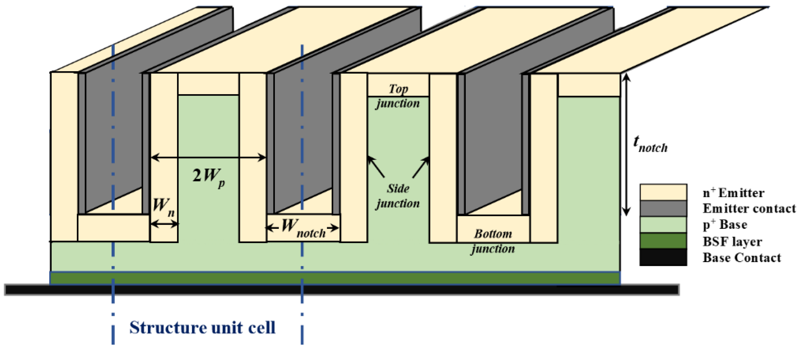
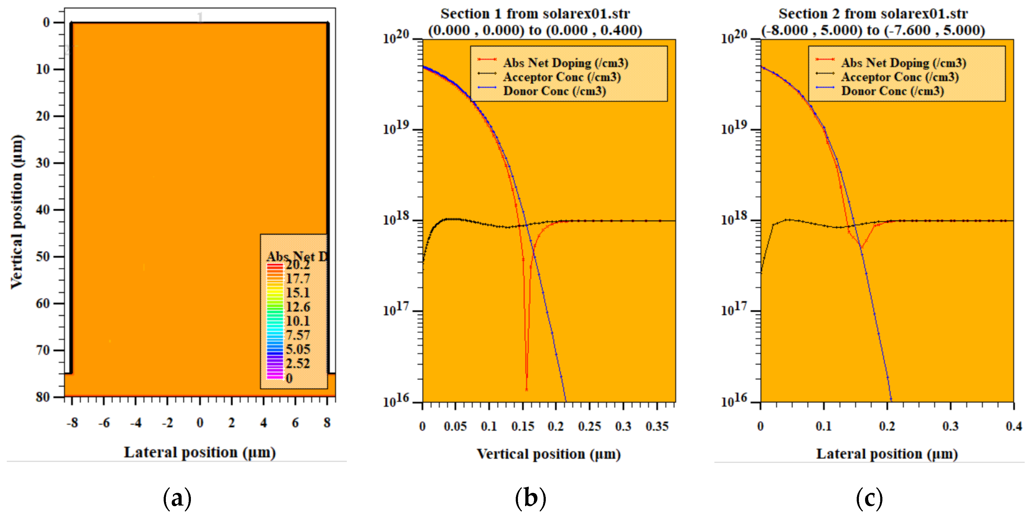
2. Materials and Methods

Figure 1 displays a 3D view of the partially-filled-notches npn SC microstructure. The primary purpose of this configuration is to remove the metal from the structure notches, unlike the conventional structure in which the notches are completely filled with metal [31,32,33,34,35]. Therefore, this modified structure has the advantage of reducing the shadowing effect, thus activating the bottom planar solar cell, which will contribute to enhancing the structure performance. Consequently, it is qualitatively expected that both the optical and electrical performance of the presented SC structure will be better than the conventional fully filled notches structure. The different p-n junctions involved in the cell are divided into the top, bottom, and side junctions. The main junctions which contribute to photon collection are the side ones; however, the top junction has a useful function of capturing the ultraviolet part of solar radiation [33], while the bottom junction enhances the short circuit current, as will be demonstrated hereafter.
The partially filled notches npn microstructure has the same technological and physical parameters as the conventional one considered in our previous work [34,35], except that the nearly open notches have a thin aluminum 0.1 µm film on the structure sidewalls, as is depicted in Figure 1. This metal layer serves as the cathode electrode of the structure. The key parameters of the structure are listed as follows (see Figure 1). The p+ base width is 2Wp, where Wp is the width of the base region that is set to Wp = 8 µm. The n+ layer thickness can be tuned according to the diffusion process via a process simulator. For our structure, it is found from our previous work that a width of the n+ side wall emitter (Wn) of about 0.18 µm gives an optimum efficiency. The thickness of the thin wafer is taken to be 80 µm. This thickness is beneficial for lowering the cost and it is actually a demand for future wafers to be less than 100 µm, as the cost of wafers is considered the most severe factor that results in increasing the PV module cost. The doping densities of the p+-base, n+-side emitter are Np+,base = 1018 cm−3 and Nn+,emitter = 5 × 1019 cm−3. Regarding the notch width and thickness, they are taken as Wnotch = 2 µm and tnotch = 75 µm. The reasons behind choosing such design values were thoroughly discussed and claimed in our previous work [31,32,33,34,35].
The simulation of the proposed solar cell is executed by exploiting the SILVACO TCAD process and device simulators, following the subsequent steps. First, the microstructure SC is realized by using a SILVACO process simulator (Athena) [47]. In the Athena process simulator, after defining the mesh, a Si wafer that acts as a substrate is defined. The doping of the substrate is p-type boron with a concentration of 1 × 1018 cm−3, while the wafer orientation is chosen to be (100). The grooves are then defined by an etching process producing open trenches that are 2 µm in width and 75 µm in depth. The n+ emitter is produced by the diffusion of phosphorous to obtain a concentration of about 5 × 1019 cm−3. Next, the sidewall electrodes are formed, and the metal is etched from the surfaces. To form the BSF and the back electrode, the wafer is flipped and the diffusion of p+ dopants and back metallization are performed, respectively. Figure 2 reveals the proposed structure, which is designed using the Athena fabrication tool. As shown, Figure 2a represents a cross-sectional view of the structure while Figure 2b,c demonstrate cutlines through the vertical and lateral directions, respectively. The doping profiles, including acceptor, donor, and absolute net doping, are shown for the top and the left lateral p-n junctions.
Next, the structure is simulated by applying the SILVACO device simulator (Atlas) [48]. The first Atlas step simulates the SC response to illumination by the AM1.5 solar spectrum. Based on this illumination, the photogeneration rates are calculated. These rates, upon integration, are used as input for the continuity equations. The numerical simulation implemented in Atlas is based on the solution at each mesh point of the basic semiconductor equations, which are Poisson’s equation and continuity equations for electrons and holes. These differential equations are iteratively and self-consistently solved by the coupled Newton numerical method to obtain the potential as well as the electron and hole concentrations. Then, the drift-diffusion model is invoked to solve for the transport properties. For these steps to be accomplished, the major physical models necessary for simulation are incorporated. These include mobility models that fulfill concentration and field dependence. The Shockley–Read–Hall (SRH) recombination model is taken to be concentration-dependent. Additionally, Fermi statistics, Auger recombination, and band gap narrowing models are activated to account for the high doping effects. The minority carrier lifetimes of the p-type base and the n-type emitter are extracted from the literature [49,50,51]. For the given design parameters, the bulk lifetime in the base is 5 µs, while in the emitter it is 8 µs.

3. Results and Discussion

In this section, we provide the simulation results of the proposed structure. First, we present a comparative study between the partially-filled-notches structure and the conventional one that has completely filled notches, showing the improvement of the presented solar cell inferred from the performance metrics of the solar cells, namely Jsc (short-circuit current), Voc (open-circuit voltage), FF (fill factor), and PCE (power conversion efficiency). Next, applying single, double, and triple ARC configurations, produced efficiency boosting results. A proposed process flow including the design of the front contact is provided, paving the way for the fabrication of the proposed structure.

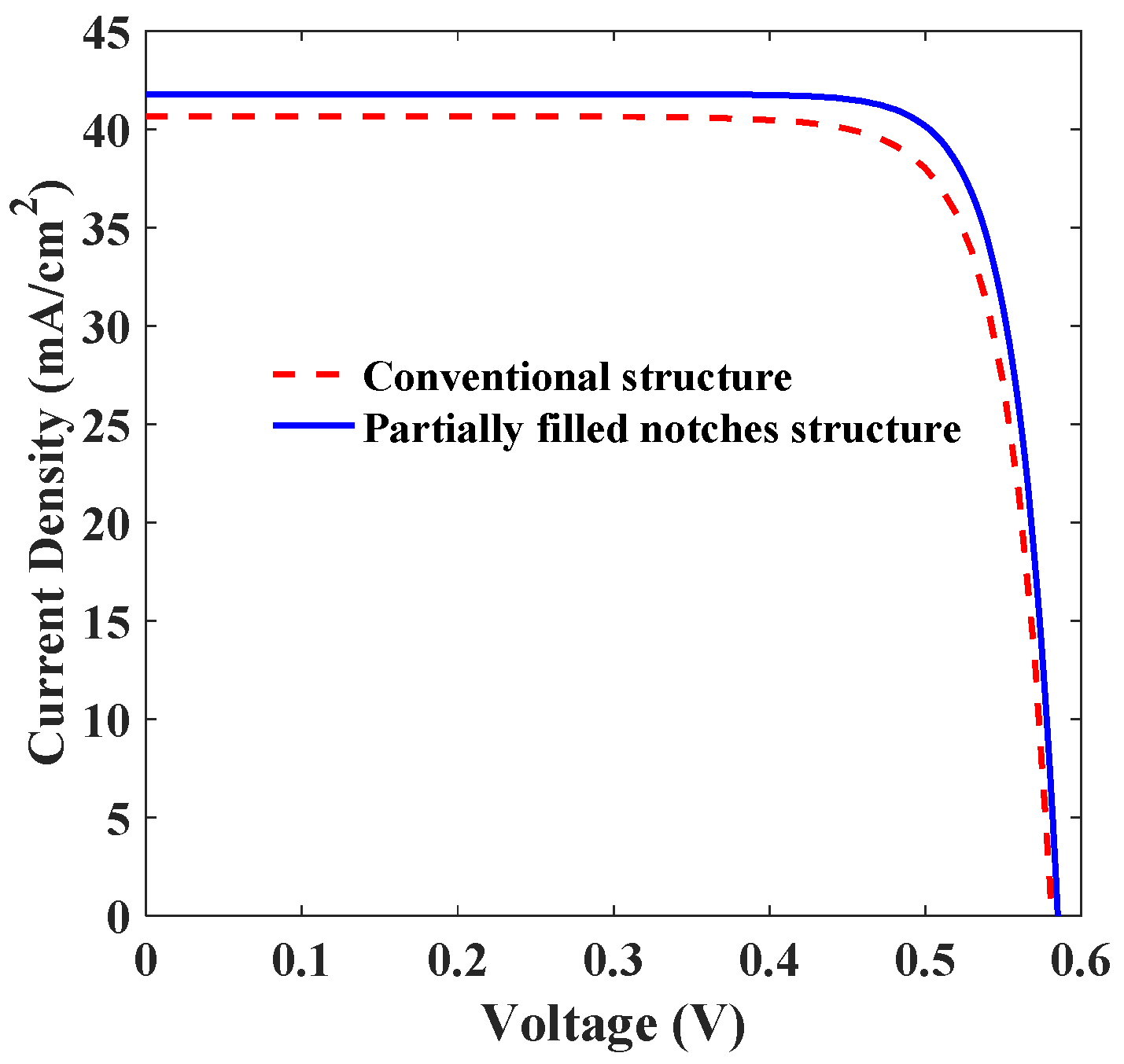
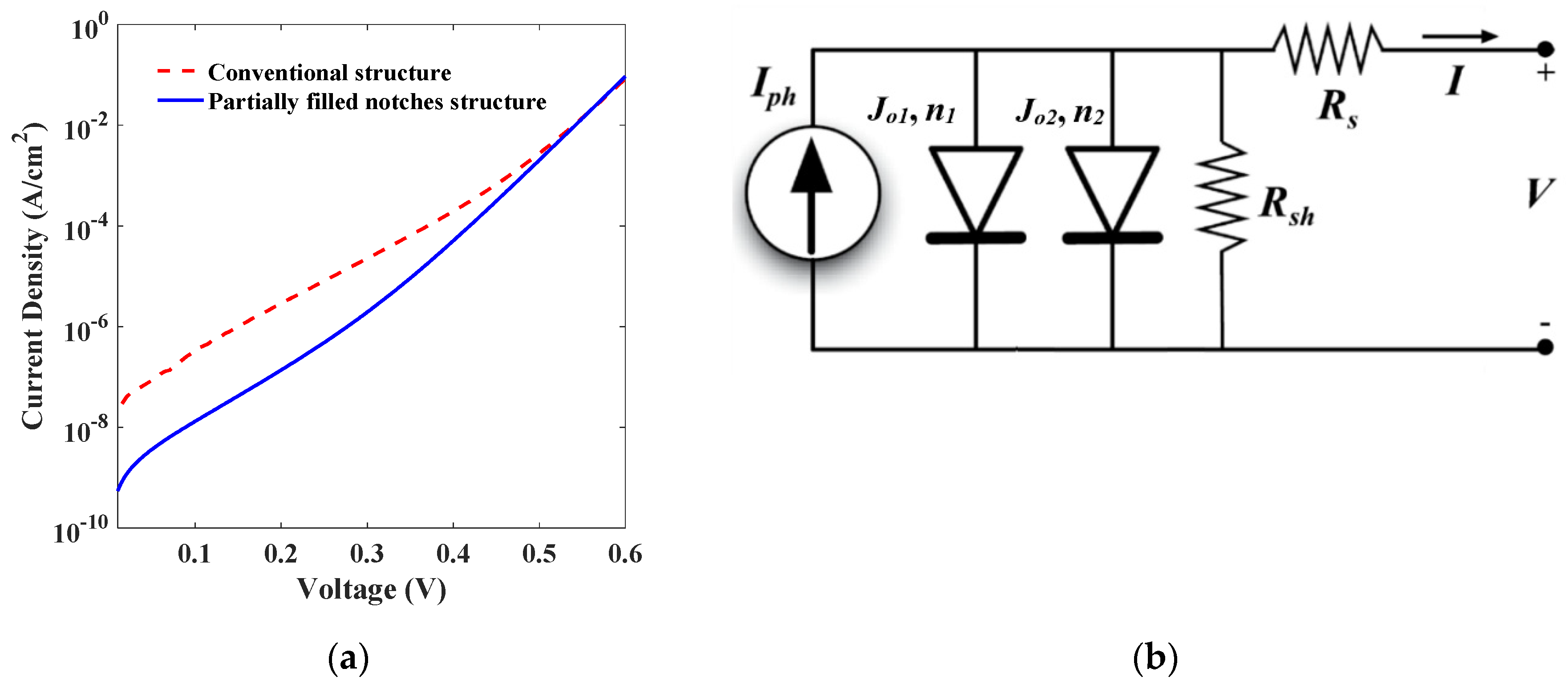
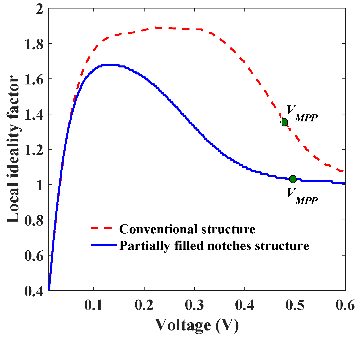
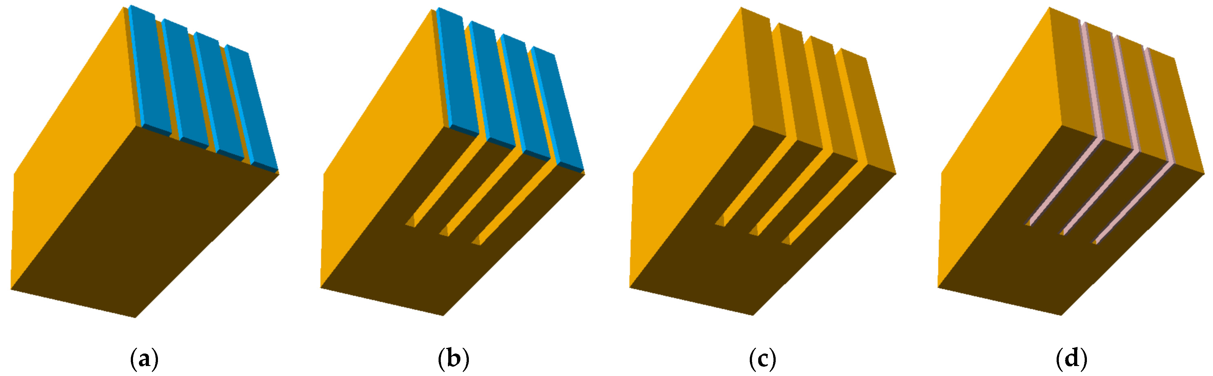
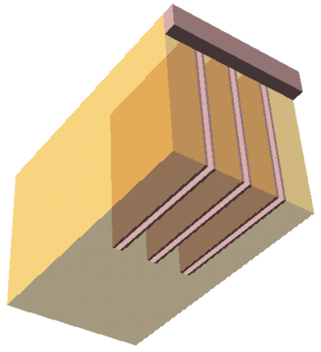
3.1. Comparison between Partially Filled and Fully Filled Notches Structures
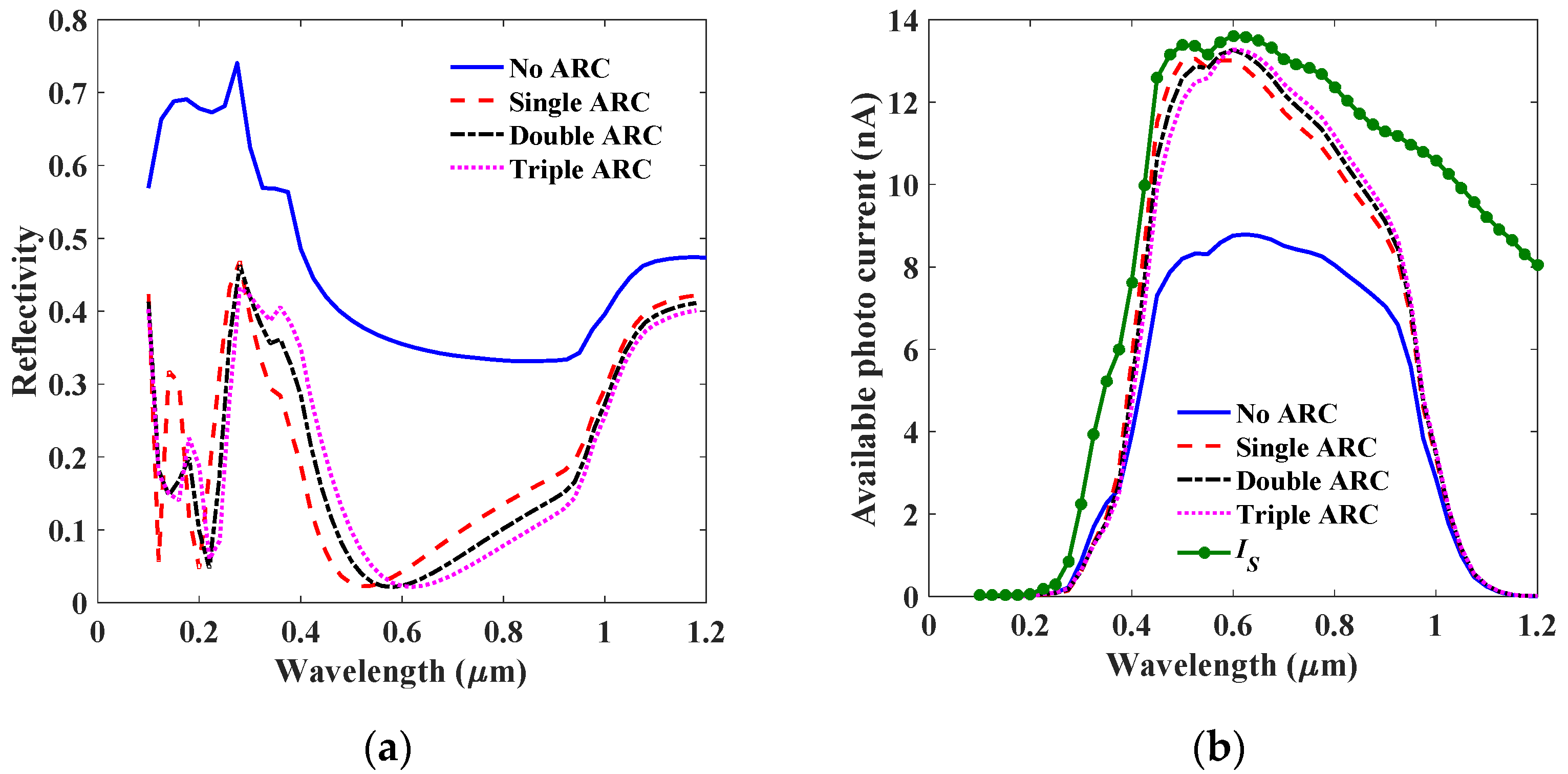
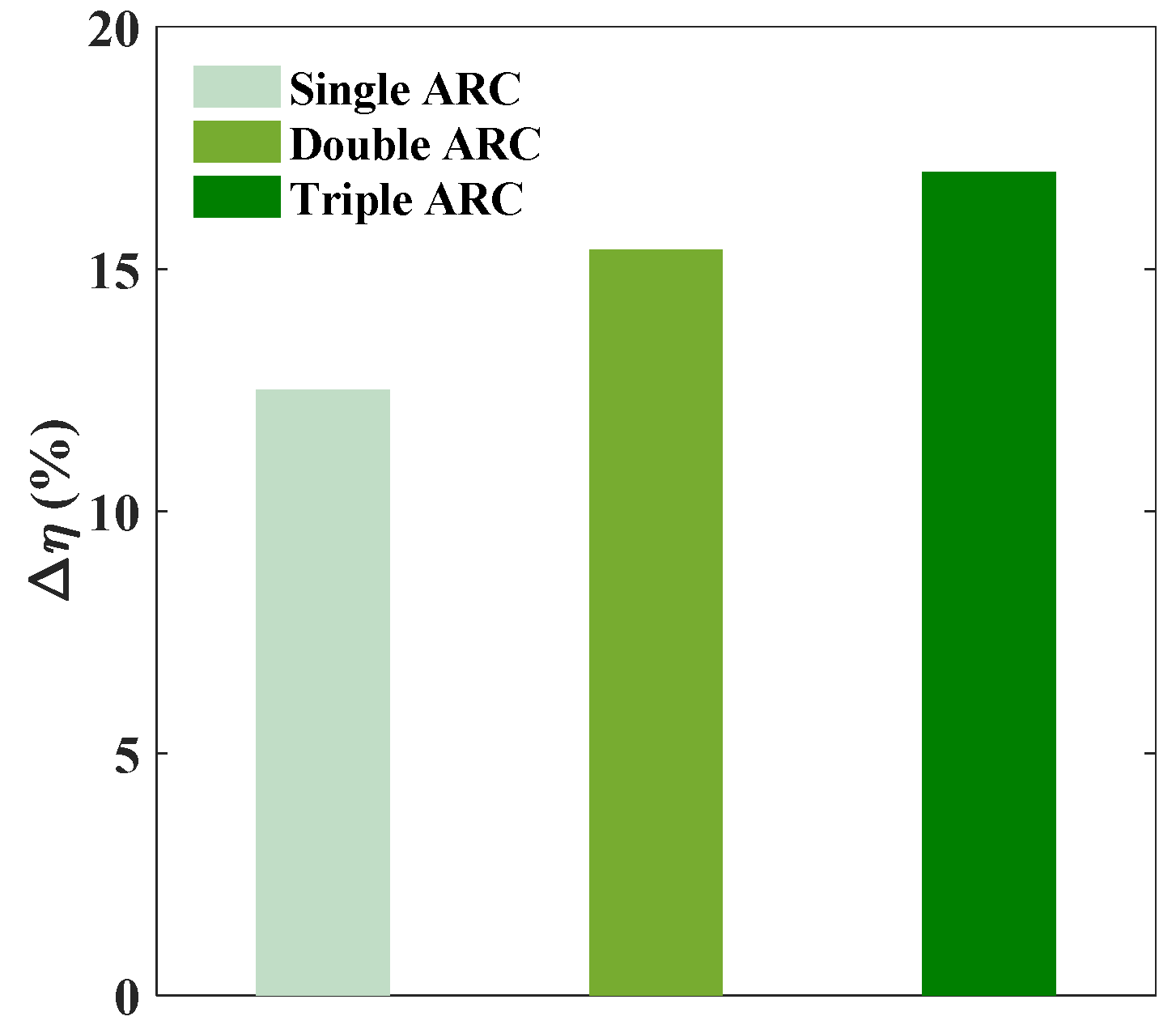
In this subsection, we present a comparative study between the electrical performance of the conventional and the partially-filled-notches npn structure. The comparison is accomplished using the Atlas device simulator. The electrical performance is examined by the illuminated current density—voltage (J–V) characteristics under the AM1.5G solar spectrum. Figure 3 shows the characteristics of both structures. A higher short circuit current for the open-notches structure is obvious because the bottom planar solar cell of the open-notches structure is activated compared to the conventional configuration. Furthermore, in Table 1, the extracted electrical performance PV parameters, Jsc, Voc, FF, and PCE, are reported for the two structures. As indicated in the table, the FF of the open notches case is higher than that of the conventional SC. This is due to the lower series resistance [52]. Based on the enhancement of Jsc and FF, a higher PCE result regarding the open notches case as it is evident in Table 1. Its efficiency is 0.8% above the conventional cell, which is considered a good enhancement.
Moreover, the dark characteristics of the two structures are simulated to obtain more physical insight into the differences between them. The simulation results are displayed in Figure 4a. For Si-based SCs, the equivalent circuit of the two-diode model can successfully explain cell behavior. A representation of the circuit is illustrated in Figure 4b. The two main factors describing the diode are the reverse saturation current (Jo) and the ideality factor (n). Each diode has its own Jo and n. the other circuit parameter is the series resistance Rs. The shunt resistance is assumed to be very large, as is evident from Figure 3. The five parameters are extracted from the dark J-V curves and are listed in Table 2. Regarding the ideality factor of the first diode, which is effective in the low voltage regime up to 0.4 V, its value regarding the modified structure is less than that of the conventional one, implying less recombination in the bulk region. Regarding the voltage range 0.5 V to 0.6 V, the ideality factor is nearly 1.0, which corresponds to an ideal diode. It might be pointed out here that an ideality factor higher than unity defines the current because of the recombination in the depletion region. On the other hand, a unity value depicts the diffusion current resulting from the recombination in the emitter and base regions of the SC [25].
Although the reverse saturation current of the first diode is lower for the case of the modified structure, the open-circuit voltage of the two structures is nearly the same. This can be explained based on the following analytical equation:
V o c n 2 V T ln ( J s c J o 2 ) ,
where VT is the thermal voltage. While Jo2 is lower and Jsc is higher, the value of n2 is higher for the partially filled structure than for the conventional cell (see Table 2), suggesting a similar Voc for the two structures. Using Equation (1), the ratio of Voc of the conventional structure to that of the modified structure is found to be nearly 1.0, which matches the simulation trend. Moreover, to explain the higher FF obtained from the modified structure over that of the conventional one, the local ideality factor can give a clear view of this change. In this regard, Figure 5 shows the local ideality factor and illustrates the points of VMPP from which the FF can be analytically calculated. It has been reported that, as the local ideality factor is higher at VMPP, for which the maximum output power occurs, a higher FF occurs [53,54]. This qualitative analysis is in agreement with the recorded values in Table 1.

3.2. ARC Techniques

In this subsection, the impact of various ARC schemes on the proposed npn SC microstructure performance is investigated. Remarkably, antireflection coating techniques play a crucial role in decreasing the front surface reflectivity. Such techniques could be significantly efficient in enhancing the optical performance of SCs, especially silicon-based cells, due to the high refractive index of silicon [36,37]. Here, single, double, and triple ARC layers are simulated to achieve minimum reflectivity and maximum available photocurrent. As a result, the conversion efficiency will be maximized. The main performance indicators, like reflectivity, as well as available and source photocurrents, are simulated and provided to give a comparative study between the different cases of ARCs.
Firstly, the effect of using a single ARC layer of ZnO is carried out. The ZnO is selected as it achieves lower reflectivity in a wider band of the wavelength in comparison with the other single-layer ARCs [55,56]. The thickness of the ZnO ARC single layer is selected to be 64 nm, which is the optimum design condition [55,56,57]. Secondly, a double ARC layer is chosen for our simulation which is based on the Si3N4/ZnO system. The thickness of the first ARC layer, which is the ZnO, is selected to be 54 nm, while that of the second layer (Si3N4) is selected to be 15 nm. Finally, a triple (SiO2/Si3N/ZnO) ARC is simulated. The thicknesses of the three layers are selected to be 15, 20, and 50 nm, respectively.
Figure 6 demonstrates the simulation results for the distinct ARC cases. Figure 6a displays the reflectivity behavior, while Figure 6b displays the available photocurrent. The source photocurrent (IS) is also shown for comparison (see Figure 6b). When comparing the case of no ARC with the single layer ZnO ARC, it is obvious that reflectivity is significantly reduced, resulting in a considerable rise in the available photocurrent. The performance metrics for the case of the double ARC technique are better than the single-layer case, as evident from Figure 6 for both reflectivity and available photocurrent above a wavelength of 0.6 µm. Additionally. it is obvious that the triple layer ARC gives the minimum reflectivity and, consequently, better performance of the SC microstructure.
Moreover, the electrical stimulation of the different ARC methods is performed to extract the PCE. The performance indicator regarding this simulation is the relative efficiency Δη, which is defined as (PCEARCPCENoARC)/PCENoARC, where PCENoARC and PCENoARC represent the efficiency without ARC and when applying ARC, respectively. Figure 7 shows the improvement in the structure conversion efficiency because of the ARC. In the single ARC case, Δη is found to be 12.5%, while it is 15.4% for the case of double ARC. In the case of the triple ARC, Δη is found to be 17%, which is considered the best performance.

3.3. Proposed Process Flow

Concerning the processability of the presented SC, the structure fabrication is straightforward, as it needs the same mature process steps as those encountered in fabricating a conventional planar SC. The extra step is to engrave vertical grooves by generating deep trenches. It is not a challenging or costly additional fabrication step, as the deep trench ion etching (DRIE) process can etch such deep trenches. In addition, the aspect ratio in the structure is 2:75, which is feasible [58].
The starting substrate could be chosen to be p-type with a high doping level in the order of 1 × 1018 cm−3. To prepare for the notches, a periodic photoresist is deposited as strip lines which have a width of 16 µm and a spacing of 2 µm, as illustrated in Figure 8a. Next, to attain a depth of about 75 µm, a deep ion reactive etching is required. This will produce micro-grating notches of 2 µm in width and 75 µm in thickness through the wafer, as represented in Figure 8b. The photoresist layers are then removed by etching, as seen in Figure 8c. The emitter is to be formed using phosphorous atoms at a concentration less than 5 × 1019 cm−3, where the junction depth should be less than 200 nm. A thickness of about 100 nm Aluminum (Al) is to be evaporated on the structure, as seen in Figure 8d, utilizing, for instance, an E-beam evaporator. After that, the top Al layer is removed by a commercial tape. The bus-bars connecting all of the emitters are evaporated to form the cathode contact. A thickness of about 500 nm of the Al back electrode is evaporated to form the anode back contact. Finally, the design of the front contact may be done via a bus-bar, like in the case of planar c-Si SC, as displayed in Figure 9. It is noted that the metal penetration for the cathode contact finger helps increase the area, which, in turn, lowers the series resistance. Therefore, the issue of designing the finger width encountered in planar SCs is not faced in our structure.
It should be pointed out here that plasmonic effects can be produced in such a periodic metallic structure, formed from the finger shape of the proposed structure, as the difference between the electrodes is in the order of 1 µm [42]. These effects may further support the light coupling into the structure and enhance the performance of the bottom p-n junction. A detailed study of these effects can be performed in individual future work.

4. Conclusions

In this research work, we introduced a proposed SC structure in which we tried to overcome both electrical and optical losses by properly designing the main cell parameters. The presented npn microstructure is designed in such a way as to alleviate the shadowing effect by opening the deep trenches. The emitter electrode is proposed to be a shallow layer, produced by evaporation for instance, instead of the complete filling of the notches with metal. This design lets the bottom p-n junction work in the same way as the top junction, implying a higher short circuit current. The performance of the proposed partially-filled-notches microstructure has been compared to that of the conventional cell, showing an improvement of 0.8% in efficiency. Further, to overcome the light reflections from the surface, we have applied different ARC techniques, namely single, double, and triple systems using ZnO, Si3N4/ZnO, and SiO2/Si3N/ZnO. It has been shown, based on simulation results, that there is a relative improvement of 12.5%, 15.4%, and 17% in the efficiency results for the single, double, and triple ARC layers, respectively. Moreover, we have discussed the suggested process flow to fabricate the proposed SC. Finally, we have provided the design of the front contact to achieve minimum electrical and optical losses. The presented study may open a path to the fabrication of a highly efficient SC which is based on low-cost Si wafers.

Author Contributions

M.S.S., A.Z., A.S., M.A. and M.M.E.-B. had a role in the conceptualization, methodology, M.S.S., A.Z. and A.S. Writing—original draft, M.A. and M.M.E.-B. Validation and investigation. M.S.S., A.Z., A.S., T.S.A. and M.T.A. contributed to software, T.S.A. and M.T.A. Formal analysis, M.S.S., A.Z. and A.S. Resources and writing—review and editing. All authors have read and agreed to the published version of the manuscript.

Funding

This research was funded by Scientific Research Deanship at University of Ha’il—Saudi Arabia, project number RG-21 023.

Data Availability Statement

Not applicable.

Acknowledgments

The authors would like to thank the Deanship of Scientific Research at the University of Ha’il for their sponsorship of the project number RG-21 023.

Conflicts of Interest

The authors declare no conflict of interest.

References

  1. Andreani, L.C.; Bozzola, A.; Kowalczewski, P.; Liscidini, M.; Redorici, L. Silicon solar cells: Toward the efficiency limits. Adv. Phys. 2019, X4, 1548305. [Google Scholar] [CrossRef]
  2. Jacak, J.E.; Jacak, W.A. Routes for Metallization of Perovskite Solar Cells. Materials 2022, 15, 2254. [Google Scholar] [CrossRef] [PubMed]
  3. Fraunhofer Institute for Solar Energy Systems. Photovoltaics Report. 2022. Available online: https://www.ise.fraunhofer.de/content/dam/ise/de/documents/publications/studies/Photovoltaics-Report.pdf (accessed on 21 September 2022).
  4. International Energy Agency. Renewables 2019, Market Analysis and Forecast from 2019 to 2024. IEA Reports. 2019. Available online: https://www.iea.org/reports/renewables-2019 (accessed on 21 September 2022).
  5. Park, J.E.; Han, C.-S.; Choi, W.S.; Lim, D. Effect of Various Wafer Surface Etching Processes on c-Si Solar Cell Characteristics. Energies 2021, 14, 4106. [Google Scholar] [CrossRef]
  6. UNIST. EPFL Claim 25.6% Efficiency World Record for Perovskite Solar Cell. PVMag. 2021. Available online: https://www.pv-magazine.com/2021/04/06/unist-epfl-claim-25-6-efficiency-world-record-for-perovskite-solar-cell/ (accessed on 21 September 2022).
  7. Ma, R.; Yan, C.; Yu, J.; Liu, T.; Liu, H.; Li, Y.; Chen, J.; Luo, Z.; Tang, B.; Lu, X.; et al. High-Efficiency Ternary Organic Solar Cells with a Good Figure-of-Merit Enabled by Two Low-Cost Donor Polymers. ACS Energy Lett. 2022, 7, 2547–2556. [Google Scholar] [CrossRef]
  8. Zhan, L.; Yin, S.; Li, Y.; Li, S.; Chen, T.; Sun, R.; Min, J.; Zhou, G.; Zhu, H.; Chen, Y.; et al. Multi-Phase Morphology with Enhanced Carrier Lifetime via Quaternary Strategy Enables High-Efficiency Thick-Film and Large-Area Organic Photovoltaics. Adv. Mater. 2022, 2206269. [Google Scholar] [CrossRef]
  9. Zhu, L.; Zhang, M.; Xu, J.; Li, C.; Yan, J.; Zhou, G.; Zhong, W.; Hao, T.; Song, J.; Xue, X.; et al. Single-junction organic solar cells with over 19% efficiency enabled by a refined double-fibril network morphology. Nat. Mater. 2022, 21, 656–663. [Google Scholar] [CrossRef]
  10. Ma, R.; Yan, C.; Fong, P.W.K.; Yu, J.; Liu, H.; Yin, J.; Huang, J.; Lu, X.; Yan, H.; Li, G. In situ and ex situ investigations on ternary strategy and co-solvent effects towards high-efficiency organic solar cells. Energy Environ. Sci. 2022, 15, 2479. [Google Scholar] [CrossRef]
  11. Jiang, X.; Chotard, P.; Luo, K.; Eckmann, F.; Tu, S.; Reus, M.A.; Yin, S.; Reitenbach, J.; Weindl, C.L.; Schwartzkopf, M.; et al. Revealing Donor–Acceptor Interaction on the Printed Active Layer Morphology and the Formation Kinetics for Nonfullerene Organic Solar Cells at Ambient Conditions. Adv. Energy Mater. 2022, 12, 2103977. [Google Scholar] [CrossRef]
  12. Luo, Z.; Ma, R.; Yu, J.; Liu, H.; Liu, T.; Ni, F.; Hu, J.; Zou, Y.; Zeng, A.; Su, C.J.; et al. Heteroheptacene-based acceptors with thieno [3, 2-b] pyrrole yield high-performance polymer solar cells. Natl. Sci. Rev. 2022, 9, nwac076. [Google Scholar] [CrossRef]
  13. Chigondo, F. From metallurgical-grade to solar-grade silicon: An overview. Silicon 2018, 10, 789–798. [Google Scholar] [CrossRef]
  14. Yoshikawa, K.; Kawasaki, H.; Yoshida, W.; Irie, T.; Konishi, K.; Nakano, K.; Uto, T.; Adachi, D.; Kanematsu, M.; Uzu, H.; et al. Silicon heterojunction solar cell with interdigitated back contacts for a photoconversion efficiency Over 26%. Nat. Energy 2017, 2, 17032. [Google Scholar] [CrossRef]
  15. Rühle, S. Tabulated values of the Shockley–Queisser limit for single junction solar cells. Sol. Energy 2016, 130, 139–147. [Google Scholar] [CrossRef]
  16. Paviet-Salomon, B.; Gall, S.; Monna, R.; Manuel, S.; Slaoui, A. Analysis of laser-doped phosphorus emitters. Energy Procedia 2011, 8, 214–219. [Google Scholar] [CrossRef]
  17. Zhang, C.; Shen, H.; Sun, L.; Yang, J.; Wu, S.; Lu, Z. Bifacial p-Type PERC Solar Cell with Efficiency over 22% Using Laser Doped Selective Emitter. Energies 2020, 13, 1388. [Google Scholar] [CrossRef]
  18. Hollemann, C.; Haase, F.; Rienäcker, M.; Barnscheidt, V.; Krügener, J.; Folchert, N.; Brendel, R.; Richter, S.; Großer, S.; Sauter, E.; et al. Separating the two polarities of the POLO contacts of an 26.1%-efficient IBC solar cell. Sci. Rep. 2020, 10, 658. [Google Scholar] [CrossRef]
  19. Okil, M.; Salem, M.S.; Abdolkader, T.M.; Shaker, A. From Crystalline to Low-cost Silicon-based Solar Cells: A Review. Silicon 2021, 14, 1895–1911. [Google Scholar] [CrossRef]
  20. Sun, H.; Deng, K.; Xiong, J.; Li, L. Graded bandgap perovskite with intrinsic n–p homojunction expands photon harvesting range and enables all transport layer-free perovskite solar cells. Adv. Energy Mater. 2020, 10, 1903347. [Google Scholar] [CrossRef]
  21. Cui, P.; Wei, D.; Ji, J.; Huang, H.; Jia, E.; Dou, S.; Wang, T.; Wang, W.; Li, M. Planar p–n homojunction perovskite solar cells with efficiency exceeding 21.3%. Nat. Energy 2019, 4, 150–159. [Google Scholar] [CrossRef]
  22. Salem, M.S.; Shaker, A.; Zekry, A.; Abouelatta, M.; Alanazi, A.; Alshammari, M.T.; Gontand, C. Analysis of hybrid hetero-homo junction lead-free perovskite solar cells by SCAPS simulator. Energies 2021, 14, 5741. [Google Scholar] [CrossRef]
  23. Sengar, B.S.; Garg, V.; Kumar, A.; Dwivedi, P. Numerical simulation: Design of high-efficiency planar pn homojunction perovskite solar cells. IEEE Trans. Electron Devices 2021, 68, 2360–2364. [Google Scholar] [CrossRef]
  24. Shaker, A.; Salem, M.S.; Jayan, K.D. Analysis and design of pn homojunction Sb2Se3 solar cells by numerical simulation. Sol. Energy 2022, 242, 276–286. [Google Scholar] [CrossRef]
  25. Zekry, A.; Shaker, A.; Salem, M. Solar cells and arrays: Principles, analysis, and design. In Advances in Renewable Energies and Power Technologies, 1st ed.; Elsevier: Amsterdam, The Netherlands, 2018; Volume 1, pp. 3–56. [Google Scholar]
  26. Garnett, E.; Yang, P. Light trapping in silicon nanowire solar cells. Nano Lett. 2010, 10, 1082–1087. [Google Scholar] [CrossRef] [PubMed]
  27. Lee, H.J. TCAD Simulation of Silicon Pillar Array Solar Cells. J. Semicond. Disp. Technol. 2017, 16, 65–69. [Google Scholar]
  28. Zhang, Y.; Liu, H. Nanowires for High-Efficiency, Low-Cost Solar Photovoltaics. Crystals 2019, 9, 87. [Google Scholar] [CrossRef]
  29. Yang, T.C.; Lee, B.S.; Yen, T.J. Minimizing reflection losses from metallic electrodes and enhancing photovoltaic performance using the Si-micrograting solar cell with vertical sidewall electrodes. Appl. Phys. Lett. 2012, 101, 103902. [Google Scholar]
  30. Zhang, Y.; Fan, Z.; Zhang, W.; Ma, Q.; Jiang, Z.; Ma, D. High performance hybrid silicon micropillar solar cell based on light trapping characteristics of Cu nanoparticles. AIP Adv. 2018, 8, 055309. [Google Scholar] [CrossRef]
  31. Salem, M.S.; Alzahrani, A.J.; Ramadan, R.A.; Alanazi, A.; Shaker, A.; Abouelatta, M.; Zekry, A. Physically based analytical model of heavily doped silicon wafers based proposed solar cell microstructure. IEEE Access 2020, 8, 138898–138906. [Google Scholar] [CrossRef]
  32. Basyoni, M.S.; Zekry, A.; Shaker, A. Investigation of base high doping impact on the npn solar cell microstructure performance using physically based analytical model. IEEE Access 2021, 9, 16958–16966. [Google Scholar] [CrossRef]
  33. Salem, M.S.; Zekry, A.; Shaker, A.; Abouelatta, M. Design and simulation of proposed low cost solar cell structures based on heavily doped silicon wafers. In Proceedings of the 2016 IEEE 43rd Photovoltaic Specialists Conference (PVSC), Portland, OR, USA, 5–10 June 2016. [Google Scholar] [CrossRef]
  34. Salem, M.S.; Zekry, A.; Abouelatta, M.; Alshammari, M.T.; Alanazi, A.; Al-Dhlan, K.A.; Shaker, A. Influence of base doping level on the npn microstructure solar cell performance: A TCAD study. Opt. Mater. 2021, 121, 111501. [Google Scholar] [CrossRef]
  35. Salem, M.S.; Zekry, A.; Shaker, A.; Abouelatta, M.; Abdolkader, T.M. Performance enhancement of a proposed solar cell microstructure based on heavily doped silicon wafers. Semicond. Sci. Technol. 2019, 34, 035012. [Google Scholar] [CrossRef]
  36. Sahouane, N.; Zerga, A. Optimization of Antireflection Multilayer for Industrial Crystalline Silicon Solar Cells. Energy Procedia 2014, 44, 118–125. [Google Scholar] [CrossRef] [Green Version]
  37. Xiao, X.J.; Zhu, H.M.; Liu, Z.M.; Tu, J.L. Multilayer antireflection coatings design for SiO2-passivated silicon solar cells. Mater. Und Werkst. 2022, 53, 80–88. [Google Scholar] [CrossRef]
  38. Swatowska, B.; Stapinski, T.; Drabczyk, K.; Panek, P. The role of antirefective coatings in silicon solar cells—the influence on their electrical parameters. Opt. Appl. 2011, 41, 487–492. [Google Scholar]
  39. Wright, D.N.; Marstein, E.S.; Holt, A. Double Layer Anti-reflective Coatings for Silicon Solar Cells. In Proceedings of the Thirty-First IEEE Photovoltaic Specialists Conference, Lake Buena Vista, FL, USA, 3–7 January 2005; pp. 1237–1240. [Google Scholar]
  40. Lennie, A.; Abdullah, H.; Shila, Z.M.; Hannan, M.A. Modeling and Simulation of SiO2/Si3N4 as Anti-reflecting Coating for Silicon Solar cell by using Silvaco Software. World Appl. Sci. J. 2010, 11, 786–790. [Google Scholar]
  41. Moradi, M.; Rajabi, Z. Efciency enhancement of Si solar cells by using nanostructured single and double layer anti-refective coatings. J. Nanostruct. 2013, 3, 365–369. [Google Scholar]
  42. Jacak, W. Quantum Nano-Plasmonics; Cambridge UP: Cambridge, UK, 2020. [Google Scholar]
  43. Abdelraouf, O.A.; Shaker, A.; Allam, N.K. Front dielectric and back plasmonic wire grating for efficient light trapping in perovskite solar cells. Opt. Mater. 2018, 86, 311–317. [Google Scholar] [CrossRef]
  44. Kumawat, U.K.; Kumar, K.; Mishra, S.; Dhawan, A. Plasmonic-enhanced microcrystalline silicon solar cells. JOSA B 2020, 37, 495–504. [Google Scholar] [CrossRef]
  45. Cortés-Juan, F.; Chaverri Ramos, C.; Connolly, J.P.; David, C.; García de Abajo, F.J.; Hurtado, J.; Mihailetchi, V.D.; Ponce-Alcántara, S.; Sánchez, G. Effect of Ag nanoparticles integrated within antireflection coatings for solar cells. J. Renew. Sustain. Energy 2013, 5, 033116. [Google Scholar] [CrossRef]
  46. Pala, R.A.; White, J.; Barnard, E.; Liu, J.; Brongersma, M.L. Design of plasmonic thin-film solar cells with broadband absorption enhancements. Adv. Mater. 2009, 21, 3504–3509. [Google Scholar] [CrossRef]
  47. Athena User’s Manual. Silvaco Inc.: Santa Clara, CA, USA; Available online: https://silvaco.com/products/tcad/process_simulation/athena/athena.html (accessed on 1 September 2022).
  48. Atlas User’s Manual. Silvaco Inc.: Santa Clara, CA, USA. Available online: https://silvaco.com/products/tcad/device_simulation/atlas/atlas.html (accessed on 1 September 2022).
  49. Zekry, A. The dependence of diffusion length, lifetime and emitter Gummel-number on temperature and doping. Arch. Für Elektrotechnik 1992, 75, 147–154. [Google Scholar] [CrossRef]
  50. del Alamo, J.A.; Swanson, R.M. Modelling of minority-carrier transport in heavily doped silicon emitters. Solid. State. Electron. 1987, 30, 1127–1136. [Google Scholar] [CrossRef]
  51. Zekry, A.; Shaker, A.; Ossaimee, M.; Salem, M.S.; Abouelatta, M.A. comprehensive semi-analytical model of the polysilicon emitter contact in bipolar transistors. J. Comput. Electron. 2018, 17, 246–255. [Google Scholar] [CrossRef]
  52. Zekry, Z.; Eldallal, G. Effect of MS contact on the electrical behaviour of solar cells. Solid-State Electron. 1988, 31, 91–97. [Google Scholar] [CrossRef]
  53. Green, M.A. Solar cell fill factors: General graph and empirical expressions. Solid-State Electron. 1981, 24, 788–789. [Google Scholar] [CrossRef]
  54. Gamal, N.; Sedky, S.H.; Shaker, A.; Fedawy, M. Design of lead-free perovskite solar cell using Zn1-xMgxO as ETL: SCAPS device simulation. Optik 2021, 242, 167306. [Google Scholar] [CrossRef]
  55. Minemoto, T.; Mizuta, T.; Takakura, H.; Hamakawa, Y. Antireflective Coating fabricated by chemical deposition of (ZnO) for spherical (Si) solar cells. J. Sol. Energy Mater. Sol. Cells 2007, 91, 191–194. [Google Scholar] [CrossRef]
  56. Naser, N.M.; Mustafa, B.T. Single layer anti-reflective (AR) coating silicon solar cells using simulation program. ZANCO J. Pure Appl. Sci. 2017, 28, 39–43. [Google Scholar]
  57. Chee, K.W.; Tang, Z.; Lü, H.; Huang, F. Anti-reflective structures for photovoltaics: Numerical and experimental design. Energy Rep. 2018, 4, 266–273. [Google Scholar] [CrossRef]
  58. Ghoneim, M.T.; Hussain, M.M. Highly manufacturable deep (sub-millimeter) etching enabled high aspect ratio complex geometry lego-like silicon electronics. Small 2017, 13, 1601801. [Google Scholar] [CrossRef] [Green Version]
Figure 1. 3D schematic representation of the partially-filled-notches npn solar cell microstructure utilized in the study.
Energies 15 07179 g001
Figure 2. The proposed microstructure generated by Athena process framework (a) cross-sectional view for a unit cell illustrating the absolute net doping, (b) vertical cutline (through x = 0 µm) to show the doping profile of the top p-n junction and (c) lateral cutline (through y = 5 µm) to show the doping profile of left p-n junction.
Energies 15 07179 g002
Figure 3. A comparison of illuminated J–V curves between the conventional and partially filled notches structures.
Energies 15 07179 g003
Figure 4. (a) A comparison between the dark characteristics of the conventional npn and partially-filled-notches structures and (b) equivalent two-diode model.
Energies 15 07179 g004
Figure 5. A comparison between the local ideality factor, derived from the dark J-V characteristics, of the conventional and modified structures.
Energies 15 07179 g005
Figure 6. Comparison between different ARC methods applied to the proposed structure (a) reflectivity and (b) available and source photo currents.
Energies 15 07179 g006
Figure 7. Relative efficiency changes utilizing various types of ARC techniques.
Energies 15 07179 g007
Figure 8. Proposed process flow of the partially-filled notches npn microstructure (a) photoresist deposition, (b) deep etching, (c) after removing photoresist, and (d) after defining side wall emitter contact.
Energies 15 07179 g008
Figure 9. 3D schematic representation of the proposed microstructure showing one busbar and finger structure.
Energies 15 07179 g009
Table 1. PV parameters of the conventional and the partially filled notches microstructures.
StructureJsc (mA/cm2)Voc (V)FF (%)PCE (%)
Conventional40.700.58080.3014.50
Open notches41.700.58282.3015.30
Table 2. Two diode model parameters for the conventional and partially-filled notches microstructures.
StructureJo1 (A/cm2)n1Jo2 (A/cm2)n2Rs (mΩcm2)
Conventional3.99 × 10−81.8476.02 × 10−130.9096.81
Open notches1.24 × 10−91.7137.03 × 10−121.0026.76
Publisher’s Note: MDPI stays neutral with regard to jurisdictional claims in published maps and institutional affiliations.

