
Investigation of Electron Transport Material-Free Perovskite/CIGS Tandem Solar Cell

 , , , ,
Abstract
:1. Introduction
2. Materials and Methods
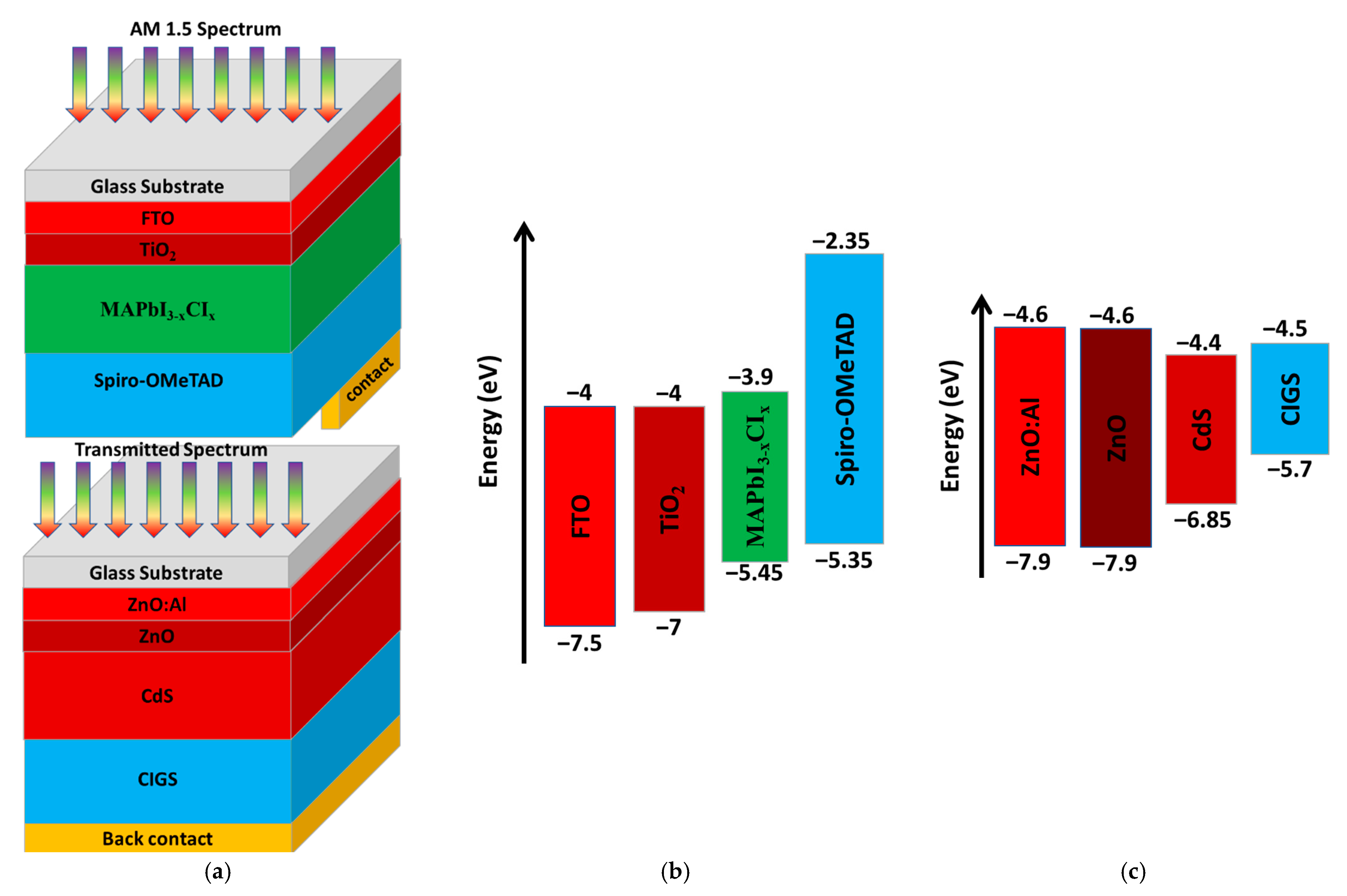
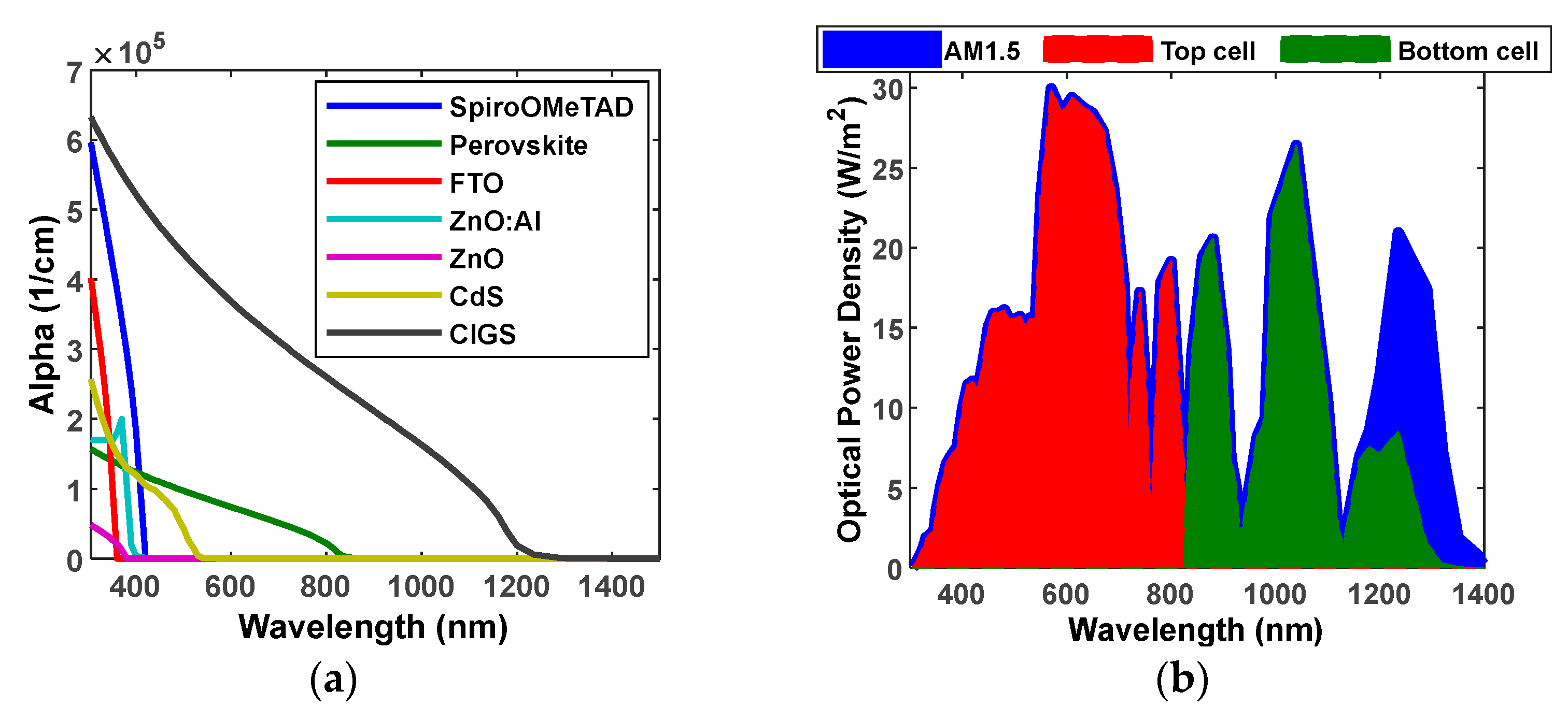
2.1. Validation of Physical Parameters Selection
3. Results and Discussions
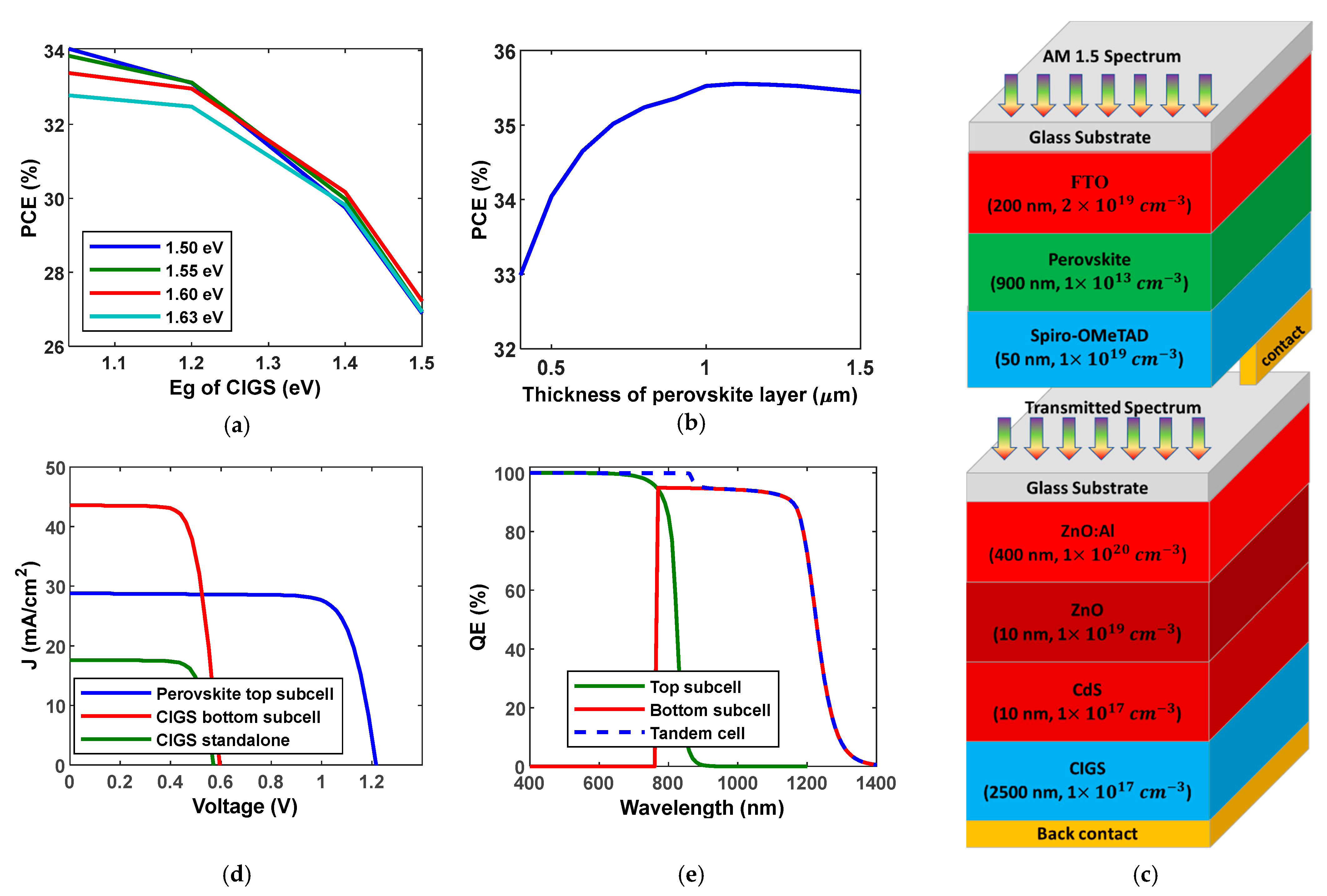
3.1. Optimization of the Sub Cells
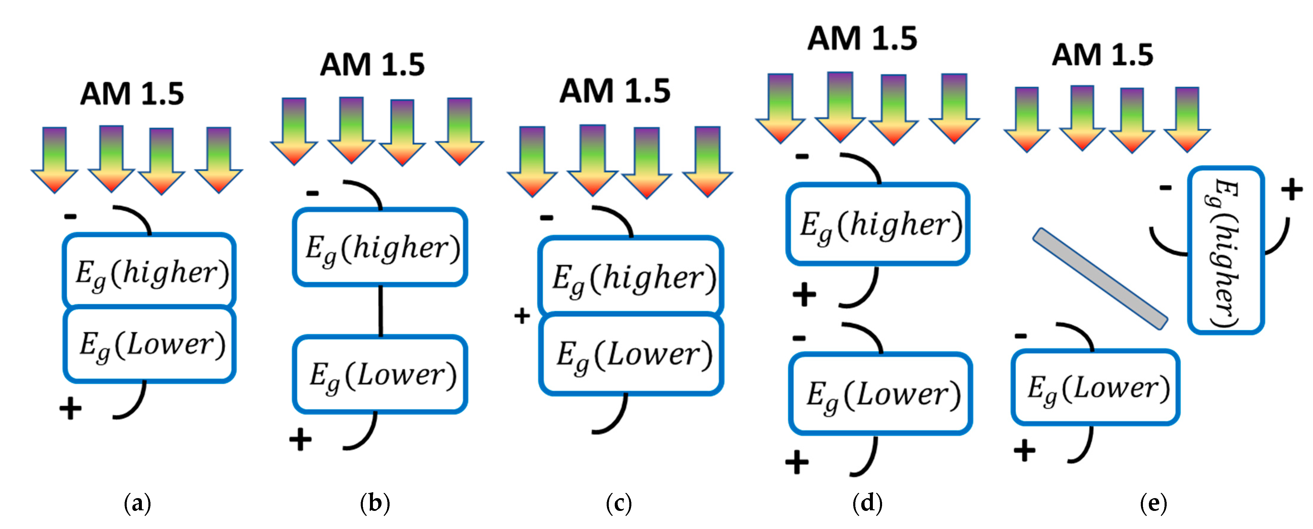
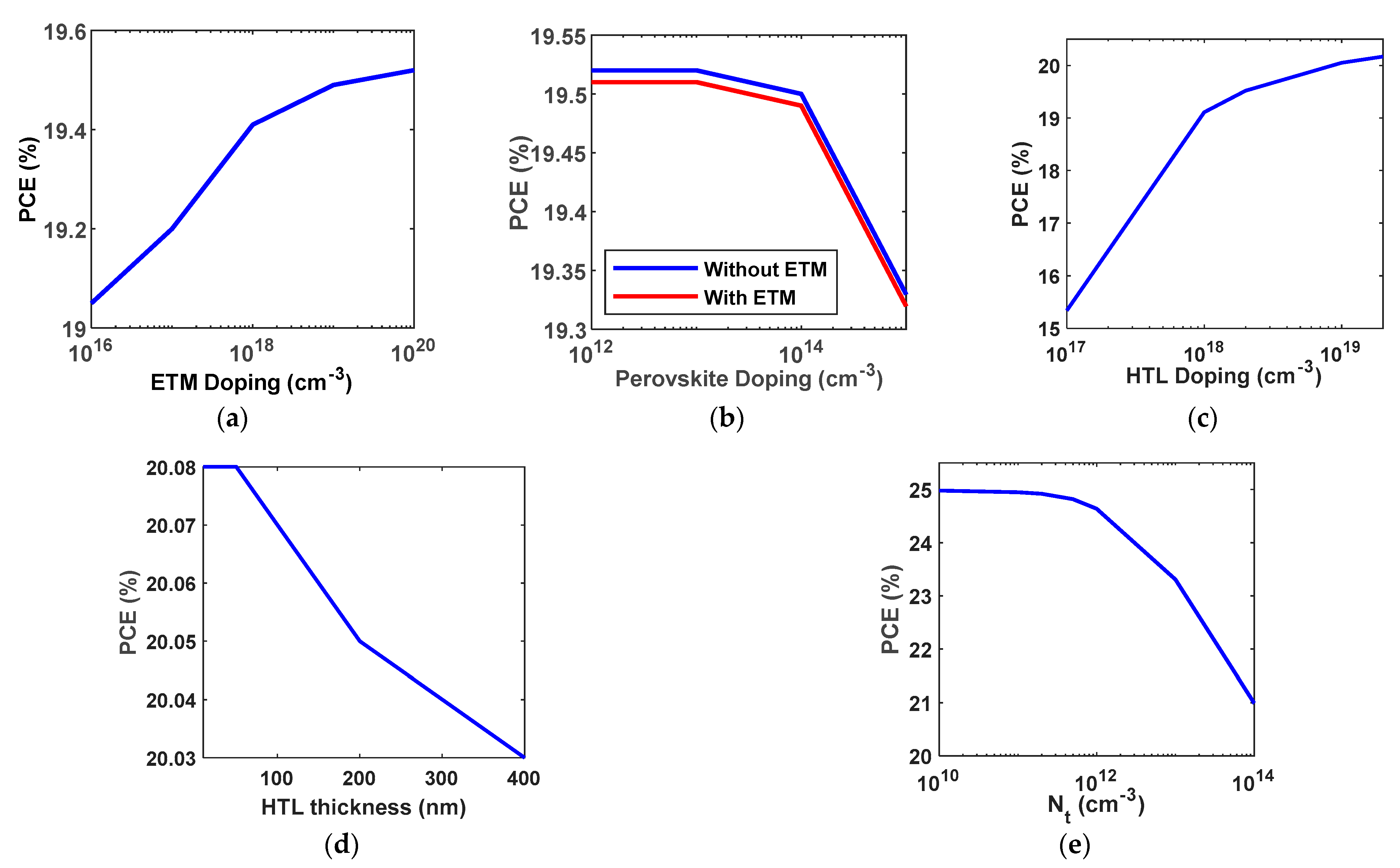
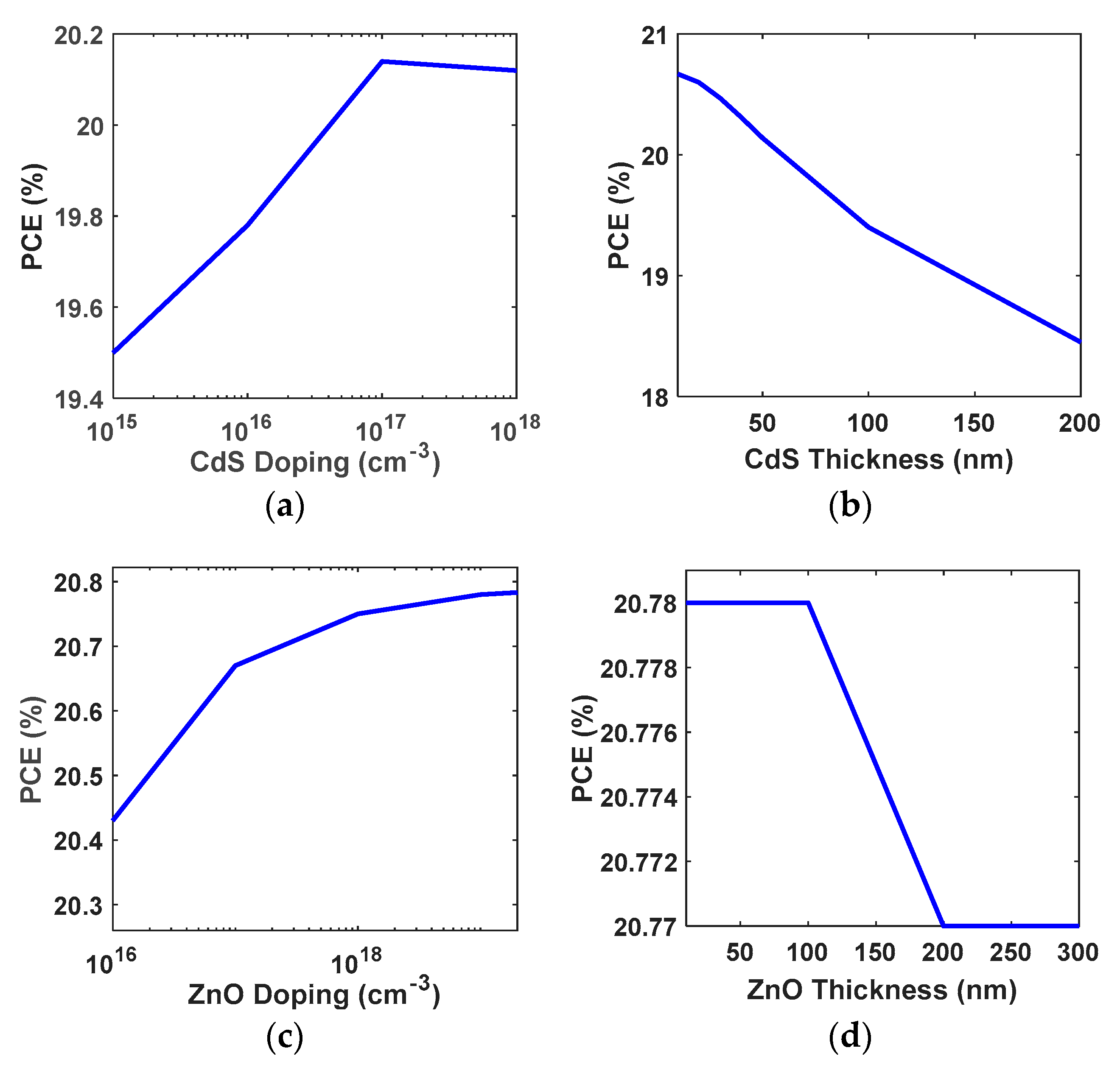
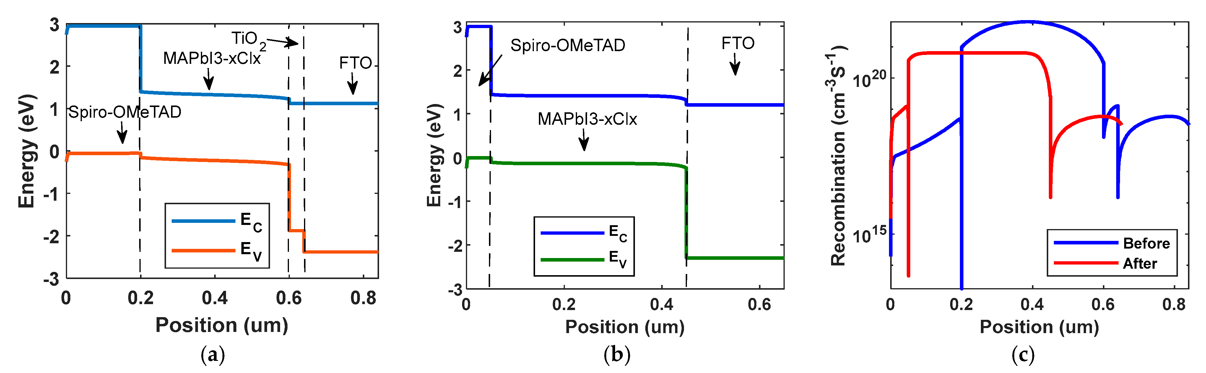
3.1.1. Optimization of the Top Sub cell
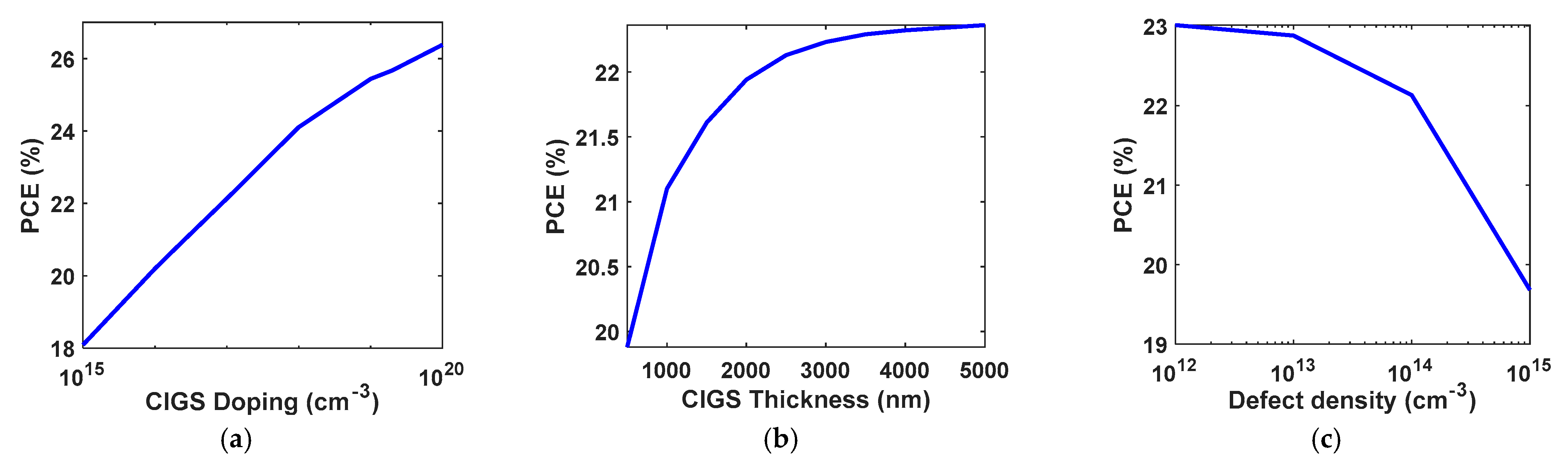
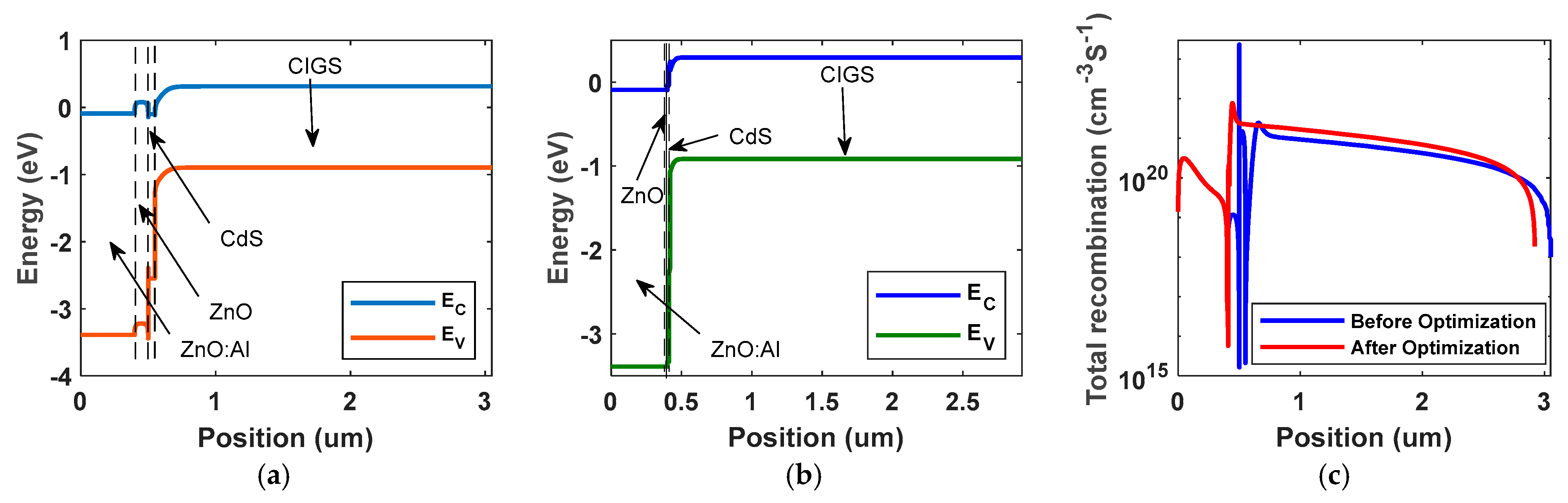
3.1.2. Optimization of the Bottom Sub Cell
3.1.3. The Initial Sub Cells vs. the Optimized Sub Cells
3.2. The Final Tandem Cell
3.3. Comparison with the State of Art Published Results
4. Conclusions
Supplementary Materials
Author Contributions
Funding
Institutional Review Board Statement
Informed Consent Statement
Data Availability Statement
Conflicts of Interest
References
- Sahbel, A.; Hassan, N.; Abdelhameed, M.M.; Zekry, A. Experimental Performance Characterization of Photovoltaic Modules Using DAQ. Energy Procedia 2013, 36, 323–332. [Google Scholar] [CrossRef]
- Zekry, A. A road map for transformation from conventional to photovoltaic energy generation and its challenges. J. King Saud Univ. Eng. Sci. 2020, 32, 407–410. [Google Scholar] [CrossRef]
- Gielen, D.; Boshell, F.; Saygin, D.; Bazilian, M.D.; Wagner, N.; Gorini, R. The role of renewable energy in the global energy transformation. Energy Strateg. Rev. 2019, 24, 38–50. [Google Scholar] [CrossRef]
- Okil, M.; Salem, M.S.; Abdolkader, T.M.; Shaker, A. From Crystalline to Low-cost Silicon-based Solar Cells: A Review. Silicon 2021, 14, 1895–1911. [Google Scholar] [CrossRef]
- Yoshikawa, K.; Kawasaki, H.; Yoshida, W.; Irie, T.; Konishi, K.; Nakano, K.; Uto, T.; Adachi, D.; Kanematsu, M.; Uzu, H.; et al. Silicon heterojunction solar cell with interdigitated back contacts for a photoconversion efficiency over 26%. Nat. Energy 2017, 2, 17032. [Google Scholar] [CrossRef]
- Nakamura, M.; Yamaguchi, K.; Kimoto, Y.; Yasaki, Y.; Kato, T.; Sugimoto, H. Cd-Free Cu(In,Ga)(Se,S)2 thin-film solar cell with record efficiency of 23.35%. IEEE J. Photovolt. 2019, 9, 1863–1867. [Google Scholar] [CrossRef]
- Yang, W.S.; Park, B.W.; Jung, E.H.; Jeon, N.J.; Kim, Y.C.; Lee, D.U.; Shin, S.S.; Seo, J.; Kim, E.K.; Noh, J.H.; et al. Iodide management in formamidinium-lead-halide-based perovskite layers for efficient solar cells. Science 2017, 356, 1376–1379. [Google Scholar] [CrossRef]
- Salah, M.M.; Abouelatta, M.; Shaker, A.; Hassan, K.M.; Saeed, A. A comprehensive simulation study of hybrid halide perovskite solar cell with copper oxide as HTM. Semicond. Sci. Technol. 2019, 34, 115009. [Google Scholar] [CrossRef]
- Han, Q.; Ding, J.; Bai, Y.; Li, T.; Ma, J.Y.; Chen, Y.X.; Zhou, Y.; Liu, J.; Ge, Q.Q.; Chen, J.; et al. Carrier Dynamics Engineering for High-Performance Electron-Transport-Layer-free Perovskite Photovoltaics. Chem 2018, 4, 2405–2417. [Google Scholar] [CrossRef]
- Yu, H.; Lee, J.W.; Yun, J.; Lee, K.; Ryu, J.; Lee, J.; Hwang, D.; Kim, S.K.; Jang, J. Outstanding Performance of Hole-Blocking Layer-Free Perovskite Solar Cell Using Hierarchically Porous Fluorine-Doped Tin Oxide Substrate. Adv. Energy Mater. 2017, 7, 1700749. [Google Scholar] [CrossRef]
- Valles-Pelarda, M.; Hames, B.C.; Inés García-Benito, I.; Almora, O.; Molina-Ontoria, A.; Sánchezsánchez, R.S.; Garcia-Belmonte, G.; Martín, N.; Mora-Sero, I. Analysis of the hysteresis behavior of perovskite solar cells with interfacial fullerene self-assembled monolayers. J. Phys. Chem. Lett. 2016, 7, 4622–4628. [Google Scholar] [CrossRef]
- Lamberti, F.; Gatti, T.; Menna, E.; Petrozza, A.; Topolovsek, P.; Lamberti, F.; Gatti, T.; Cito, A.; Ball, J.M.; Menna, E.; et al. Functionalization of transparent conductive oxide electrode for TiO 2-free perovskite solar cells. J. Mater. Chem. A 2017, 5, 11882–11893. [Google Scholar] [CrossRef]
- Huang, C.; Lin, P.; Fu, N.; Liu, C.; Xu, B.; Sun, K.; Wang, D.; Zeng, X.; Ke, S. Facile fabrication of highly efficient ETL-free perovskite solar cells with 20% efficiency by defect passivation and interface engineering. Chem. Commun. 2019, 55, 2777–2780. [Google Scholar] [CrossRef] [PubMed]
- Shockley, W.; Queisser, H.J. Detailed balance limit of efficiency of p-n junction solar cells. J. Appl. Phys. 1961, 32, 510–519. [Google Scholar] [CrossRef]
- Yasodharan, R.; Senthilkumar, A.P.; Mohankumar, P.; Ajayan, J.; Sivabalakrishnan, R. Investigation and influence of layer composition of tandem perovskite solar cells for applications in future renewable and sustainable energy. Optik 2020, 212, 164723. [Google Scholar] [CrossRef]
- De Vos, A. Detailed balance limit of the efficiency of tandem solar cells. J. Phys. D Appl. Phys. 1980, 13, 839–846. [Google Scholar] [CrossRef]
- Todorov, T.; Gunawan, O.; Guha, S. A road towards 25% efficiency and beyond: Perovskite tandem solar cells. Mol. Syst. Des. Eng. 2016, 1, 370–376. [Google Scholar] [CrossRef]
- Abdelaziz, W.; Zekry, A.; Shaker, A.; Abouelatta, M. Numerical study of organic graded bulk heterojunction solar cell using SCAPS simulation. Sol. Energy 2020, 211, 375–382. [Google Scholar] [CrossRef]
- Burgelman, M.; Decock, K.; Khelifi, S.; Abass, A. Advanced electrical simulation of thin film solar cells. Thin Solid Films 2013, 535, 296–301. [Google Scholar] [CrossRef]
- Burgelman, M.; Decock, K.; Niemegeers, A.; Verschraegen, J.; Degrave, S. SCAPS Manual; University of Gent: Ghent, Belgium, 2014. [Google Scholar]
- Yun, S.; Qin, Y.; Uhl, A.R.; Vlachopoulos, N.; Yin, M.; Li, D.; Han, X.; Hagfeldt, A. New-generation integrated devices based on dye-sensitized and perovskite solar cells. Energy Environ. Sci. 2018, 11, 476–526. [Google Scholar] [CrossRef]
- Bailie, C.D.; Greyson Christoforo, M.; Mailoa, J.P.; Bowring, A.R.; Unger, E.L.; Nguyen, W.H.; Burschka, J.; Pellet, N.; Lee, J.Z.; Grätzel, M.; et al. Semi-transparent perovskite solar cells for tandems with silicon and CIGS. Energy Environ. Sci. 2018, 8, 956–963. [Google Scholar] [CrossRef]
- Yang Michael, Y.; Chen, Q.; Hsieh, Y.T.; Bin Song, T.; De Marco, N.; Zhou, H.; Yang, Y. Multilayer Transparent Top Electrode for Solution Processed Perovskite/Cu(In,Ga)(Se,S)2 Four Terminal Tandem Solar Cells. ACS Nano 2015, 9, 7714–7721. [Google Scholar] [CrossRef]
- Hoke, E.T.; Slotcavage, D.J.; Dohner, E.R.; Bowring, A.R.; Karunadasa, H.I.; Mcgehee, M.D. Reversible photo-induced trap formation in mixed-halide hybrid perovskites for photovoltaics. Chem. Sci. 2015, 6, 613–617. [Google Scholar] [CrossRef]
- Fu, F.; Feurer, T.; Jäger, T.; Avancini, E.; Bissig, B.; Yoon, S.; Buecheler, S.; Tiwari, A.N. ARTICLE Low-temperature-processed efficient semi-transparent planar perovskite solar cells for bifacial and tandem applications. Nat. Commun. 2015, 6, 8932. [Google Scholar] [CrossRef]
- Guchhait, A.; Dewi, H.A.; Leow, S.W.; Wang, H.; Han, G.; Bin Suhaimi, F.; Mhaisalkar, S.; Wong, L.H.; Mathews, N. Over 20% Efficient CIGS-Perovskite Tandem Solar Cells. ACS Energy Lett. 2017, 2, 807–812. [Google Scholar] [CrossRef]
- Kranz, L.; Abate, A.; Feurer, T.; Fu, F.; Avancini, E.; Löckinger, J.; Reinhard, P.; Zakeeruddin, S.M.; Grätzel, M.; Buecheler, S.; et al. High-efficiency polycrystalline thin film tandem solar cells. J. Phys. Chem. Lett. 2015, 6, 2676–2681. [Google Scholar] [CrossRef]
- Gharibzadeh, S.; Hossain, I.M.; Fassl, P.; Nejand, B.A.; Abzieher, T.; Schultes, M.; Ahlswede, E.; Jackson, P.; Powalla, M.; Schäfer, S.; et al. 2D/3D Heterostructure for Semitransparent Perovskite Solar Cells with Engineered Bandgap Enables Efficiencies Exceeding 25% in Four-Terminal Tandems with Silicon and CIGS. Adv. Funct. Mater. 2020, 30, 1909919. [Google Scholar] [CrossRef]
- Chen, C.-W.; Hsiao, S.-Y.; Chen, C.-Y.; Kang, H.-W.; Huang, Z.-Y.; Lin, H.-W. Optical properties of organometal halide perovskite thin fi lms and general device structure design rules for perovskite single and tandem solar cells. J. Mater. Chem. A 2015, 3, 9152–9159. [Google Scholar] [CrossRef]
- Kim, K.; Gwak, J.; Ahn, S.K.; Eo, Y.J.; Park, J.H.; Cho, J.S.; Kang, M.G.; Song, H.E.; Yun, J.H. Simulations of chalcopyrite/c-Si tandem cells using SCAPS-1D. Sol. Energy 2017, 145, 52–58. [Google Scholar] [CrossRef]
- Mandadapu, U.; Vedanayakam, S.V.; Thyagarajan, K. Simulation and Analysis of Lead based Perovskite Solar Cell using SCAPS-1D. Indian J. Sci. Technol. 2017, 10, 65–72. [Google Scholar] [CrossRef]
- Ding, Y.; Shi, B.; Yao, X.; Fan, L.; Luo, J.; Wei, C.; Zhang, D.; Wang, G.; Sheng, Y.; Chen, Y.; et al. Elucidating the role of chlorine in perovskite solar cells. J. Mater. Chem. A 2017, 5, 7423–7432. [Google Scholar] [CrossRef]
- Samiee, M.; Konduri, S.; Ganapathy, B.; Kottokkaran, R.; Abbas, H.A.; Kitahara, A.; Joshi, P.; Zhang, L.; Noack, M.; Dalal, V. Defect density and dielectric constant in perovskite solar cells. Appl. Phys. Lett. 2014, 105, 153502. [Google Scholar] [CrossRef]
- Li, X.; Yang, J.; Jiang, Q.; Chu, W.; Zhang, D.; Zhou, Z.; Xin, J. Synergistic Effect to High-Performance Perovskite Solar Cells with Reduced Hysteresis and Improved Stability by the Introduction of Na-Treated TiO2 and Spraying-Deposited CuI as Transport Layers. ACS Appl. Mater. Interfaces 2017, 9, 41354–41362. [Google Scholar] [CrossRef]
- Jackson, P.; Hariskos, D.; Lotter, E.; Paetel, S.; Wuerz, R.; Menner, R.; Wischmann, W.; Powalla, M. New world record efficiency for Cu(In,Ga)Se2 thin-film solar cells beyond 20%. Prog. Photovolt. Res. Appl. 2011, 19, 894–897. [Google Scholar] [CrossRef]
- Basyoni, M.S.S.; Salah, M.M.; Mousa, M.; Shaker, A.; Zekry, A.; Abouelatta, M.; Alshammari, M.T.; Al-Dhlan, K.A.; Gontrand, C. On the Investigation of Interface Defects of Solar Cells: Lead-Based vs Lead-Free Perovskite. IEEE Access 2021, 9, 130221–130232. [Google Scholar] [CrossRef]
- Etgar, L.; Gao, P.; Xue, Z.; Peng, Q.; Chandiran, A.K.; Liu, B.; Nazeeruddin, M.K.; Grätzel, M. Mesoscopic CH 3NH 3PbI 3/TiO 2 heterojunction solar cells. J. Am. Chem. Soc. 2012, 134, 17396–17399. [Google Scholar] [CrossRef] [PubMed]
- Bansal, S.; Aryal, P. Evaluation of new materials for electron and hole transport layers in perovskite-based solar cells through SCAPS-1D simulations. In Proceedings of the 2016 IEEE 43rd Photovoltaic Specialists Conference (PVSC), Portland, OR, USA, 5–10 June 2016; pp. 0747–0750. [Google Scholar] [CrossRef]
- Gupta, G.K.; Dixit, A. Theoretical studies of single and tandem Cu2ZnSn(S/Se)4 junction solar cells for enhanced efficiency. Opt. Mater. 2018, 82, 11–20. [Google Scholar] [CrossRef]
- Madan, J.; Shivani; Pandey, R.; Sharma, R. Device simulation of 17.3% efficient lead-free all-perovskite tandem solar cell. Sol. Energy 2020, 197, 212–221. [Google Scholar] [CrossRef]
- Du, H.-J.; Wang, W.-C.; Zhu, J.-Z. Device simulation of lead-free CH3NH3SnI3 perovskite solar cells with high efficiency. Chin. Phys. B 2016, 25, 108802. [Google Scholar] [CrossRef]
- Niemegeers, A.; Burgelman, M. Numerical modelling of ac-characteristics of CdTe and CIS solar cells. In Proceedings of the Conference Record of the Twenty Fifth IEEE Photovoltaic Specialists Conference, Washington, DC, USA, 13–17 May 1996. [Google Scholar] [CrossRef]
- Asaduzzaman, M.; Hasan, M.; Bahar, A.N. An investigation into the effects of band gap and doping concentration on Cu(In,Ga)Se2 solar cell efficiency. Springerplus 2016, 5, 578. [Google Scholar] [CrossRef]
- Pudov, A.O.; Kanevce, A.; Al-Thani, H.A.; Sites, J.R.; Hasoon, F.S. Secondary barriers in CdS- CuIn1-x Gax Se2 solar cells. J. Appl. Phys. 2005, 97, 064901. [Google Scholar] [CrossRef]
- Tverjanovich, A.; Borisov, E.N.; Vasilieva, E.S.; Tolochko, O.V.; Vahhi, I.E.; Bereznev, S.; Tveryanovich, Y.S. CuInSe2 thin films deposited by UV laser ablation. Sol. Energy Mater. Sol. Cells 2006, 90, 3624–3632. [Google Scholar] [CrossRef]
- Mahon, N.S.; Korolik, O.V.; Khenkin, M.V.; Arnaoutakis, G.E.; Galagan, Y.; Soriūtė, V.; Litvinas, D.; Ščajev, P.; Katz, E.A.; Mazanik, A.V. Photoluminescence kinetics for monitoring photoinduced processes in perovskite solar cells. Sol. Energy 2020, 195, 114–120. [Google Scholar] [CrossRef]
- Salah, M.M.; Zekry, A.; Abouelatta, M.; Shaker, A.; Mousa, M.; Amer, F.Z.; Mubarak, R.I.; Saeed, A. High-Efficiency Electron Transport Layer-Free Perovskite/GeTe Tandem Solar Cell: Numerical Simulation. Crystals 2022, 12, 878. [Google Scholar] [CrossRef]
- Wang, Q.; Shao, Y.; Xie, H.; Lyu, L.; Liu, X.; Gao, Y.; Huang, J. Qualifying composition dependent p and n self-doping in CH3NH3PbI3. Appl. Phys. Lett. 2014, 105, 163508. [Google Scholar] [CrossRef]
- Tan, K.; Lin, P.; Wang, G.; Liu, Y.; Xu, Z.; Lin, Y. Controllable design of solid-state perovskite solar cells by SCAPS device simulation. Solid-State Electron. 2016, 126, 75–80. [Google Scholar] [CrossRef]
- Kim, H.; Lim, K.G.; Lee, T.W. Planar heterojunction organometal halide perovskite solar cells: Roles of interfacial layers. Energy Environ. Sci. 2016, 9, 12–30. [Google Scholar] [CrossRef]
- Zekry, A.; Shaker, A.; Salem, M. Solar Cells and Arrays: Principles, Analysis, and Design. Adv. Renew. Energies Power Technol. 2018, 1, 3–56. [Google Scholar] [CrossRef]
- Kirchartz, T.; Krückemeier, L.; Unger, E.L. Research Update: Recombination and open-circuit voltage in lead-halide perovskites. APL Mater. 2018, 6, 100702. [Google Scholar] [CrossRef]
- Shi, D.; Adinolfi, V.; Comin, R.; Yuan, M.; Alarousu, E.; Buin, A.; Chen, Y.; Hoogland, S.; Rothenberger, A.; Katsiev, K.; et al. Low trap-state density and long carrier diffusion in organolead trihalide perovskite single crystals. Science 2015, 347, 519–522. [Google Scholar] [CrossRef]
- Salem, M.S.; Zekry, A.; Shaker, A.; Abouelatta, M.; Abdolkader, T.M. Performance enhancement of a proposed solar cell microstructure based on heavily doped silicon wafers. Semicond. Sci. Technol. 2019, 34, 035012. [Google Scholar] [CrossRef]
- Salem, M.S.; Shaker, A.; Zekry, A.; Abouelatta, M.; Alanazi, A.; Alshammari, M.T.; Gontand, C. Analysis of Hybrid Hetero-Homo Junction Lead-Free Perovskite Solar Cells by SCAPS Simulator. Energies 2021, 14, 5741. [Google Scholar] [CrossRef]
- Minemoto, T.; Murata, M. Theoretical analysis on effect of band offsets in perovskite solar cells. Sol. Energy Mater. Sol. Cells 2015, 133, 8–14. [Google Scholar] [CrossRef]
- Haider, S.Z.; Anwar, H.; Wang, M. A comprehensive device modelling of perovskite solar cell with inorganic copper iodide as hole transport material. Semicond. Sci. Technol. 2018, 33, 035001. [Google Scholar] [CrossRef]
- Salah, M.M.; Hassan, K.M.; Abouelatta, M.; Shaker, A. A comparative study of different ETMs in perovskite solar cell with inorganic copper iodide as HTM. Optik 2019, 178, 958–963. [Google Scholar] [CrossRef]
- Wang, N.; Zhao, K.; Ding, T.; Liu, W.; Ahmed, A.S.; Wang, Z.; Tian, M.; Sun, X.W.; Zhang, Q. Improving Interfacial Charge Recombination in Planar Heterojunction Perovskite Photovoltaics with Small Molecule as Electron Transport Layer. Adv. Energy Mater. 2017, 7, 1700522. [Google Scholar] [CrossRef]
- Gu, P.-Y.; Wang, N.; Wang, C.; Zhou, Y.; Long, G.; Tian, M.; Chen, W.; Sun, X.W.; Kanatzidis, M.G.; Zhang, Q. Pushing up the efficiency of planar perovskite solar cells to 18.2% with organic small molecules as the electron transport layer. J. Mater. Chem. A 2017, 5, 7339–7344. [Google Scholar] [CrossRef]
- Lin, L.; Li, P.; Jiang, L.; Kang, Z.; Yan, Q.; Xiong, H.; Lien, S.; Zhang, P.; Qiu, Y.; Energy, S.L.-S.; et al. Boosting efficiency up to 25% for HTL-free carbon-based perovskite solar cells by gradient doping using SCAPS simulation. Sol. Energy 2021, 215, 328–334. [Google Scholar] [CrossRef]
- Chae, J.; Dong, Q.; Huang, J.; Centrone, A. Chloride Incorporation Process in CH3NH3PbI3-xClx Perovskites via Nanoscale Bandgap Maps. Nano Lett. 2015, 15, 8114–8121. [Google Scholar] [CrossRef]
- Iefanova, A.; Adhikari, N.; Dubey, A.; Khatiwada, D.; Qiao, Q. Lead free CH3NH3SnI3 perovskite thin-film with p-type semiconducting nature and metal-like conductivity. AIP Adv. 2016, 6, 085312. [Google Scholar] [CrossRef]
- Jäger, K.; Tillmann, P.; Katz, E.A.; Becker, C. Perovskite/Silicon Tandem Solar Cells: Effect of Luminescent Coupling and Bifaciality. Sol. RRL 2021, 5, 2000628. [Google Scholar] [CrossRef]
- Köhnen, E.; Wagner, P.; Lang, F.; Cruz, A.; Li, B.; Roß, M.; Jošt, M.; Morales-Vilches, A.B.; Topič, M.; Stolterfoht, M.; et al. 27.9% Efficient Monolithic Perovskite/Silicon Tandem Solar Cells on Industry Compatible Bottom Cells. Sol. RRL 2021, 5, 2100244. [Google Scholar] [CrossRef]
- Tockhorn, P.; Berlin, H.-Z.; Sutter, J.; Cruz, A.; Wagner, P.; Jäger, K.; Yoo, D.; Lang, F.; Grischek, M.; Li, B.; et al. Nano-optical designs enhance monolithic perovskite/silicon tandem solar cells toward 29.8% efficiency. Res. Sq. 2022, 49, 1–16. [Google Scholar] [CrossRef]
- Ferhati, H.; Djeffal, F. Exceeding 30% efficiency for an environment-friendly tandem solar cell based on earth-abundant Se/CZTS materials. Phys. E Low-Dimens. Syst. Nanostruct. 2019, 109, 52–58. [Google Scholar] [CrossRef]
- Mousa, M.; Salah, M.M.; Amer, F.Z.; Saeed, A.; Mubarak, R.I. High Efficiency Tandem Perovskite/CIGS Solar Cell. In Proceedings of the 2020 2nd International Conference on Smart Power & Internet Energy Systems (SPIES), Bangkok, Thailand, 15–18 September 2020; pp. 224–227. [Google Scholar] [CrossRef]
- Benaicha, M.; Dehimi, L.; Pezzimenti, F.; Bouzid, F. Simulation analysis of a high efficiency GaInP/Si multijunction solar cell. J. Semicond. 2020, 41, 032701. [Google Scholar] [CrossRef]
- Essig, S.; Allebé, C.; Remo, T.; Geisz, J.F.; Steiner, M.A.; Horowitz, K.; Barraud, L.; Ward, J.S.; Schnabel, M.; Descoeudres, A.; et al. Raising the one-sun conversion efficiency of III–V/Si solar cells to 32.8% for two junctions and 35.9% for three junctions. Nat. Energy 2017, 2, 17144. [Google Scholar] [CrossRef]
- Shen, H.; Jacobs, D.A.; Wu, Y.; Duong, T.; Peng, J.; Wen, X.; Fu, X.; Karuturi, S.K.; White, T.P.; Weber, K.; et al. Inverted Hysteresis in CH3NH3PbI3 Solar Cells: Role of Stoichiometry and Band Alignment. J. Phys. Chem. Lett. 2017, 8, 2672–2680. [Google Scholar] [CrossRef] [PubMed]


| Parameters | FTO [36] | MAPbI3−xCIx [37,38] | Spiro-OMeTAD [10,39,40] | TiO2 [38,41,42] | CIGS [35,43,44,45] | CdS [44] | ZnO [44] | ZnO-Al [44] |
|---|---|---|---|---|---|---|---|---|
| Band gap energy Eg (eV) | 3.5 | 1.55 | 3 | 3 | 1.04–1.67 | 2.45 | 3.30 | 3.30 |
| Thickness (nm) | 200 | Fitting | 200 | 50 | 2000–3000 | 50 | 100 | 400 |
| Relative permittivity ɛr | 9 | 6.5 | 3 | 10 | 13.6 | 10.0 | 9.0 | 9.0 |
| Electron affinity (eV) | 4 | 3.9 | 2.35 | 4 | 4.5 | 4.4 | 4.6 | 4.6 |
| Effective conduction band density Nc (cm−3) | 2.2 × 10¹⁸ | 3 × 10¹⁸ | ||||||
| Electron mobility µe (cm−2 V−1 s−1) | 20 | 2 | 2 × 10⁻⁴ | 20 | 100 | |||
| Donor concentration ND (cm−3) | 2 × 10¹⁹ | 0 | 0 | 1018 | 0 | 1020 | 1017 | 1020 |
| Effective valence band density Nv (cm−3) | 18 × 1017 | 1.8 × 10¹⁹ | 1.7 × 10¹⁹ | |||||
| Hole mobility µp (cm−2 V−1 s−1) | 10 | 2 | 2 × 10⁻⁴ | 10 | 25 | 25 | 25 | 31 |
| Acceptor concentration NA (cm−3) | 0 | 0 | 2 × 10¹⁸ | 0 | 2×10¹⁶ | 0 | 0 | 0 |
| Defect density Nt (cm−3) | 1015 | 2 × 10¹⁴ | 1015 | 1015 | 1014 | 1014–5 × 10¹⁶ | 1014 | 1014–1016 |
| Thermal velocity of electrons vth,n (cm/s) | 107 | 2.4 × 10⁷ | ||||||
| Thermal velocity of holes vth,p (cm/s) | 1.3 × 10⁷ | |||||||
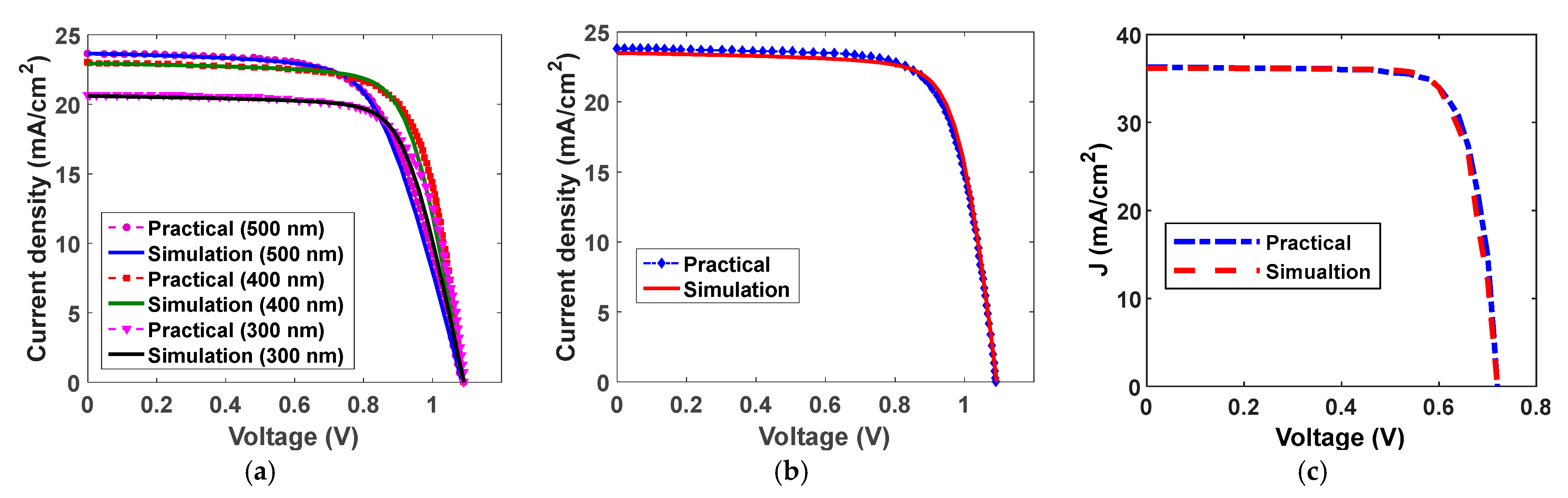
| Absorber | Type | PCE (%) | Jsc (mA/cm2) | Voc (V) | FF (%) |
|---|---|---|---|---|---|
| Perovskite | Experimental | 19.41 | 23.80 | 1.09 | 75.16 |
| Simulation | 19.41 | 23.50 | 1.09 | 75.55 | |
| CIGS | Experimental | 20.10 | 36.30 | 0.72 | 76.80 |
| Simulation | 20.08 | 36.22 | 0.72 | 77.05 |
| ETM/HTM | PCE (%) |
|---|---|
| TiO2/CuI [57] | 21.32 |
| TiO2/CuI [58] | 21.76 |
| ZnOS/CuI [58] | 26.11 |
| PEDOT:PSS/HATNT [59] | 18.10 |
| PEDOT:PSS/TDTP [60] | 18.20 |
| TiO2/- [61] | 25.15 |
| nanoparticle based SnO2/Spiro-OMeTAD [28] | 17.90 |
| TiO2/Spiro-OMeTAD [32] | 19.41 |
| -/Spiro-OMeTAD [optimized] | 27.13 |
| PCE (%) | The Material of Top/Bottom Sub Cells | Ref.-Year |
|---|---|---|
| 25 | Perovskite/CIGS | [28]-2020 |
| 25.7 | Perovskite/C-Si | [28]-2020 |
| 29.8 | Perovskite/Si | [66]-2022 |
| 30.2 | Se/CZTSSe | [67]-2019 |
| 30.5 | MAPbI3/CIGS | [68]-2020 |
| 31.1 | GaInP/Si | [69]-2020 |
| 33.3 | Triple-junction (Ga0.51 In0.49 P/GaAs/Si) | [67]-2018 |
| 35.36 | MAPbI3−xClx without ETM/CIGS | This work |
| 35.9 | Triple-junction (GaInP/GaAs/Si) | [70]-2017 |
| 39.2 | Six-junction (monolithic) | [34]-2017 |
| 30.2 | Se/CZTSSe | [67]-2019 |
Publisher’s Note: MDPI stays neutral with regard to jurisdictional claims in published maps and institutional affiliations. |
© 2022 by the authors. Licensee MDPI, Basel, Switzerland. This article is an open access article distributed under the terms and conditions of the Creative Commons Attribution (CC BY) license (https://creativecommons.org/licenses/by/4.0/).
Share and Cite
Salah, M.M.; Zekry, A.; Shaker, A.; Abouelatta, M.; Mousa, M.; Saeed, A. Investigation of Electron Transport Material-Free Perovskite/CIGS Tandem Solar Cell. Energies 2022, 15, 6326. https://doi.org/10.3390/en15176326
Salah MM, Zekry A, Shaker A, Abouelatta M, Mousa M, Saeed A. Investigation of Electron Transport Material-Free Perovskite/CIGS Tandem Solar Cell. Energies. 2022; 15(17):6326. https://doi.org/10.3390/en15176326
Chicago/Turabian StyleSalah, Mostafa M., Abdelhalim Zekry, Ahmed Shaker, Mohamed Abouelatta, Mohamed Mousa, and Ahmed Saeed. 2022. "Investigation of Electron Transport Material-Free Perovskite/CIGS Tandem Solar Cell" Energies 15, no. 17: 6326. https://doi.org/10.3390/en15176326