Article

Simulation of Triple-Cation Perovskite Solar Cells: Key Design Factors for Efficiency Promotion

1
Department of Physics, College of Science, Northern Border University, Arar 73222, Saudi Arabia
2
Department of Physics, Faculty of Science, University of Khartoum, Khartoum 11115, Sudan
*
Author to whom correspondence should be addressed.
Energies 2023, 16(6), 2717; https://doi.org/10.3390/en16062717
Submission received: 17 February 2023 / Revised: 4 March 2023 / Accepted: 13 March 2023 / Published: 14 March 2023
(This article belongs to the Special Issue Modeling and Simulation of Solar Cells)

Abstract

:
Compositional engineering is considered one of the recent interesting techniques used in the field of perovskite solar cells (PSCs). In this method, more than one material was used in a specific cation in the perovskite structure. This work aims to simulate the cesium-containing triple-cation perovskite (TCP) via the SCAPS-1D simulation program with a device structure of ITO/SnO2/TCP/Spiro-OMeTAD/Au. First, we studied the effect of interface defects on the PCSs with respect to experimental results and found that when no interface defects occur, the power conversion efficiency (PCE) reaches a value of 22.16% which is higher than the reported PCE, implying that the fabricated cell suffers from the interface defects as a main effect on cell degradation. Incorporating interface defects into the simulation results in a very good match between the experimental and simulated data with a PCE of 17.92%. Further, to provide possible routes to enhance the performance of the solar cell under investigation, impacts of absorber layer thickness, conduction band offset (CBO), surface recombination velocity, and light intensity were explored. In addition, hole transport layer (HTL)-free design was investigated to alleviate the instability issues associated to the organic HTL, leading to a PCE of 18.28%, for a surface velocity of 104 cm/s, which is interestingly higher than the initial cell. The provided study reveals the critical role of interface defects and other key design factors and suggests potential solutions to alleviate the subsequent degradation mechanisms, thereby enhancing the overall cell performance.

1. Introduction

The traditional approach of electricity generation using fossil fuel cannot be considered as a prospective energy source for future use because of increasing carbon-dioxide emission into the atmosphere [1]. Thus, the progress of other alternatives for sustainable energy generation is required. In this context, photovoltaic (PV) solar cells have been recognized as one of the prominent contenders to accomplish sustainable and renewable sources [2,3]. The first-generation crystalline silicon (c-Si) solar cells have progressive efficiencies with time where a power conversion efficiency (PCE) of higher than 25% is obtained [4]. However, the cost-to-efficiency is not an optimum choice when considering c-Si solar cells. Although many efforts have been devoted to lower the cost, the PCE of the developed Si-based cells lags behind conventional solar cells [5,6,7,8]. Thus, other choices such as thin film solar cells (TFSCs) have been investigated and have drawn interest. One of the most suitable and attractive materials utilized in TFSCs is the perovskite material. Device structures of p–i–n heterojunction and p–n homojunction or hybrid hetero homojunction solar cells have been researched [9,10,11,12,13,14]. It is thought that perovskite solar cells (PSCs) are considered the greatest favorable next-generation paradigm for PV technologies [15].
The organic–inorganic perovskite materials have been introduced thanks to their great optical properties, adjustable bandgaps, long minority lifetimes, long diffusion lengths, as well as easy and low-cost fabrication processes [16]. Further, high PCEs have been reported in the literature for PSCs that exceed 25% [17]. Notably, perovskite materials are represented by the crystal structure of ABX3 [18]. In this formula, the A-site cation is monovalent (including methylammonium (MA+), formamidinium (FA+), cesium (Cs+), potassium (K+), and rubidium (Rb+)), while the B-site cation is divalent (including lead (Pb2+), tin (Sn2+), and germanium (Ge2+)), and X-site is a halogen anion (including iodide (I¯), bromide (Br¯), and chloride (Cl)) [19,20,21]. Recently, compositional engineering was introduced to manufacture PSCs [22,23,24,25,26,27]. Here, more than one material was used to create the solar device. Pellet et al. fabricated a perovskite composition by mixing FA and MA in the A-site to create a final composition of (MA)x(FA)1-xPbI3, leading to a significant enhancement in the structural, optical, and electrical properties of the device with a PCE of 14.9% [28]. Another composition of MA0.7FA0.3Pb(I0.9Br0.1)3 was established by Yang et al., where they used two materials in the A and X sites that showed improved morphology and boost carrier lifetime achieving a PCE of 17.34% [29]. Moreover, Tarek et al. showed a mixed-cation perovskite composition containing Cs+, FA+, and MA+ in the A-site, and mixed I and Br in the X-site creating a final composition of Cs0.05FA0.79MA0.15PbI2.45Br0.55 leading to a PCE of about 18.4% [30].
In a standard perovskite solar cell, the electron transport layer (ETL) offers a proper way to extract electrons towards the electrode; however, this extraction process is influenced by the defects at the ETL/perovskite interface. Likewise, the hole transport layer (HTL) provides an extraction path for the holes, but interfacial defects at the perovskite/HTL interface can hinder this extraction process. It has been commonly reported that interfacial defects at the interface between the ETL/perovskite or the HTL/perovskite profoundly impact cell performance [31]. So, it is crucial to avoid interface defects by properly designing the ETL/perovskite and HTL/perovskite interfaces in order to enhance the physical mechanisms of charge transportation and extraction [32]. Numerous studies have been published that propose practical methods to improve the interface either between the ETL/perovskite or perovskite/HTL. These include specific doping of the ETL, inserting a proper buffer between the HTL and the perovskite to engineer the lattice mismatch, and defect passivation strategies [33,34,35,36,37]. Recently, a hydro-functional material was developed that acts as an HTL which provides an effective hole extraction mechanism and results in lowering the interfacial charge recombination [38]. It was also revealed that MXene-based TiO2 as an ETL can enhance the interface quality and relieve lattice strain [39]. Other methodologies for device improvement through the suppression of interface defects have been reviewed in the literature [40].
Simulation studies are now indispensable for designing and expecting the performance of TFSCs before going to fabrication attempts. Various technological parameters can be easily optimized by employing TCAD simulation tools. In this regard, the one-dimensional Solar Cell Capacitance Simulator (SCAPS-1D) is an extremely valuable program to design and investigate distinctive TFSCs. The SCAPS-1D software package has been widely used and verified against experimental studies. It was used for the simulation of lead-free environmentally benign methylammonium tin-iodide (CH3NH3SnI3)-based solar cells for high-efficiency performance purposes [41,42,43]. In addition, lead-free double perovskite materials along with double ETL have been explored [44]. Advanced physical phenomena, such as interface defects, graded bandgap, and new device structures, have been also investigated by utilizing SCAPS-1D [45,46,47]. Until now, there has been no reported research on the numerical simulation of cesium-containing triple-cation perovskite solar cells (TCPSCs). Additionally, as far as our literature review extends, this is the first report revealing the role of interface defects and HTL-free for TCPSCs.
Here, to extend and understand some physical behavior beyond our previous experimental work [30], we present a simulation study using the SCAPS-1D program. First, a comparative evaluation of the model performance parameters’ values with experimental and simulated values at room temperature in the presence of interface defects, and those without interface defects, was performed. Based on this study, it was demonstrated that the role of interface defects is very critical to understand the performance of the fabricated device. Another critical aspect is to understand the relationship between device parameters and absorber layer thickness. Therefore, the thickness of the absorber layer was explored with respect to PSCs performance. This method allows a comprehensive examination of each parameter in solar cells and thus identifies the optimal conditions of operating. In addition, the impact of light intensity was incorporated to determine the cell performance under low-level intensities and how lower intensity can deteriorate cell performance. Finally, the solar cell device under study is designed to be free from an HTL. In this case, the absorber, as a p-type, is considered an HTL besides its main role. Excluding HTL organic materials is of great importance to alleviate the instability issues, thereby increasing the feasibility of commercialized PSCs. Thus, the current research study not only reveals the main degradation issue of a fabricated cell but also highlights possible ways to boost the efficiency of such a promising triple-cation PSC by engineering various key design factors.

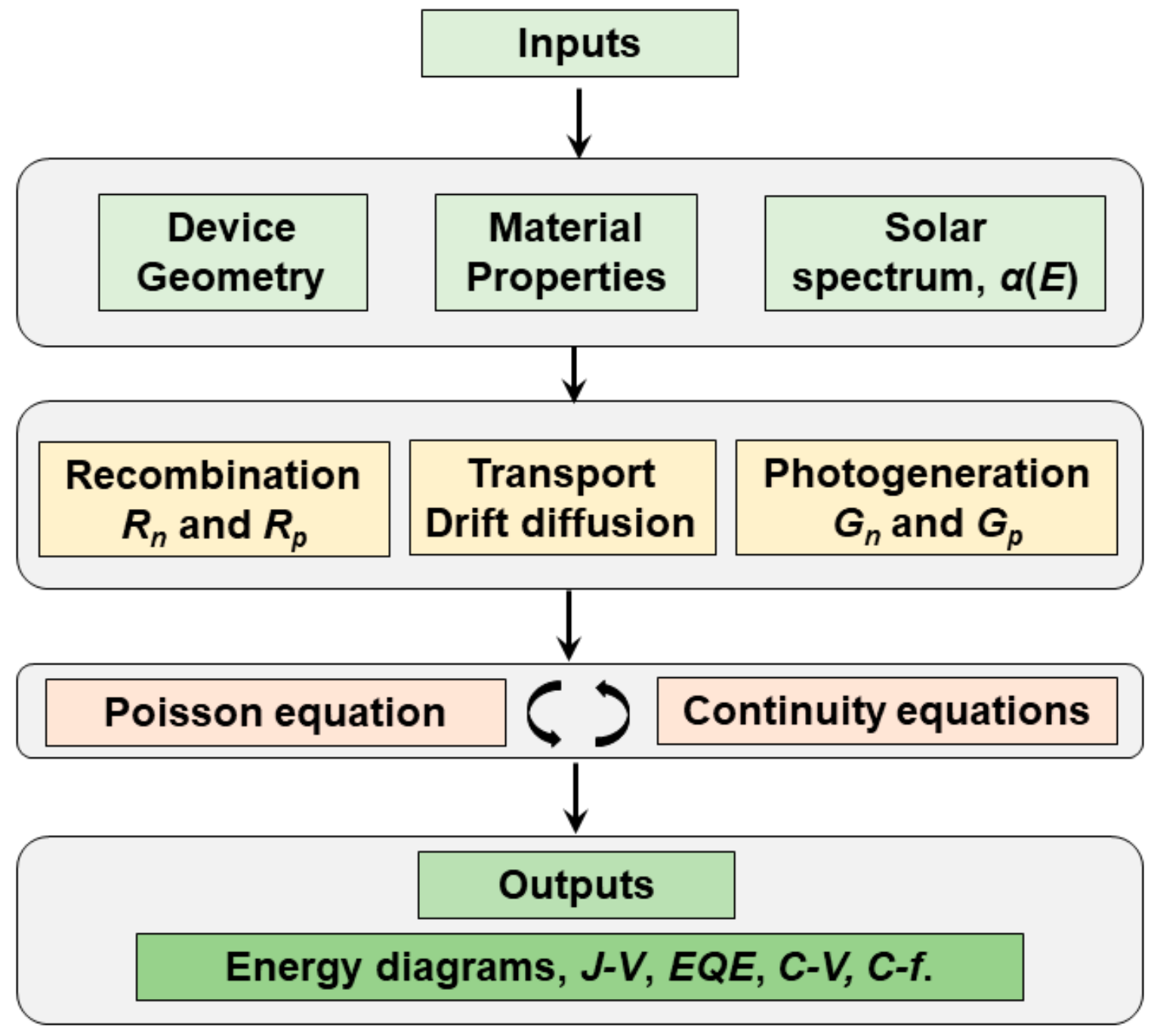
2. Modeling and Simulation Method

The SCAPS-1D package is based on physical models that are formulated mathematically to simultaneously simulate the optical and electrical properties of a TFSC. The software was developed at ELIS, University of Gent [48]. The SCAPS-1D code solves the three primary solar cell equations (using the Newton–Raphson Method): Poisson’s Equation (1), and the continuity equations for electrons and holes (Equations (2) and (3)), respectively:
d d x   ε x d ψ d x = q p x n x + N D + x N A x + p t x n t x
1 q d J n d x = G o p x + R x
1 q d J p d x = G o p x R x
where the ε is the permittivity and q is the magnitude of the charge of an electron, ψ is the electrostatic potential, and n, p, nt, and pt are the free electron, free hole, trapped electron, and trapped hole, respectively. N D + is the ionized donor-like doping concentration and N A is the ionized acceptor-like doping concentration. J n and J p are the electron and hole current densities, respectively. G o p is the optical generation rate and R x is the net recombination rate. The recombination through deep traps inside the energy gap is treated by Shockley Read Hall (SRH) recombination model [49]. The SRH recombination bulk defects are characterized by bulk electron and hole lifetimes (τn and τp). Moreover, the interface recombination can be defined between any two adjacent layers. The interfacial recombination is modeled by Pauwels–Vanhoutte theory [50], where thermionic emission is involved in its implementation. Here, the interface recombination defects are characterized by interface recombination velocities (Sn and Sp).
Two additional equations are also incorporated to relate the electron and hole quasi-Fermi levels ( E F n , and E F p ) to the electron and hole current densities as provided in Equations (4) and (5):
J n = n μ n q E F n x
J p = + p μ p q E F p x
here μ n and μ p are the electron and hole mobility, respectively. The involved equations as well as inputs to and outputs from the simulator are illustrated in a simplified flowchart in Figure 1. The solar spectrum chosen is the standard AM1.5G (1000 W/m2), and the absorption coefficient is α, which is defined as a function of energy according to the well-known square root relationship [48]. For each layer involved in the simulation, some basic parameters are inputted such as thickness, relative dielectric permittivity (εr), bandgap (Eg), electron affinity (χ), conduction band effective density of state (DOS) (NC), valence band effective DOS (NV), μp, and μn. Additionally, information about the acceptor concentration (NA) or the donor concentration (ND) is provided. Both bulk and interface defects are also defined. The output from the simulator, shown in Figure 1, can be physical quantities such as energy band diagram, recombination rates, electric field, etc., or terminal characteristics such as J-V, C-V, EQE, etc. [48].

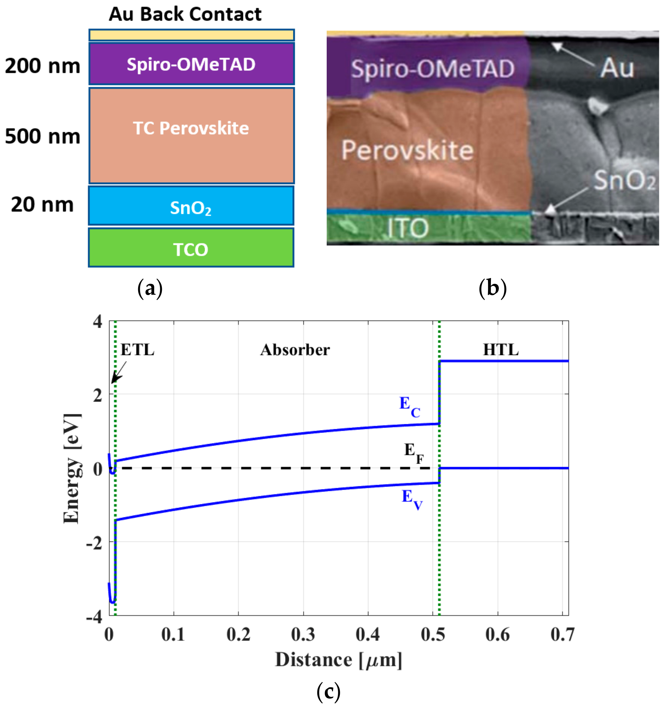
3. Device Structure and Material Parameters

The triple-cation perovskite solar cell device is designed as shown in Figure 2a where the main material parameters and layer specifications are extracted from our previous experimental work [30]. Moreover, a cross-section SEM image showing the different layers of the TCPCS is displayed in Figure 2b [30]. The absorber layer is the Cs-FA-MA-Pb(I-Br)3 (500 nm) with tin oxide (SnO2) (20 nm) and spiro-OMeTAD (200 nm) as ETL and HTL, respectively. The front and back electrical contacts are respectively indium tin oxide (ITO) and gold (Au), characterized by work functions −4.4 eV and −5.1 eV, respectively [51,52]. Furthermore, the simulated energy band diagram under the dark condition with no bias is displayed in Figure 2c. The general device parameters used in simulation are provided in Table 1 [30,53,54,55,56,57]. The simulations were carried out at temperature of 300 K under standardized conditions of illumination (air mass of AM1.5G).

4. Results and Discussion

In this section, we provide the simulation results of various case studies. First, we present a calibration step to verify the modeling methodology applied in SCAPS-1D. Next, the impact of the absorber thickness variation is investigated to determine the most suitable thickness to achieve a maximum PCE. Then, the impact of conduction band offset (CBO) and surface recombination velocity between the ETL/absorber interface is thoroughly explored. The change in intensity is also explored. Finally, the HTL-free design is introduced as a recommendation for minimizing the instability issues related to the organic HTL.

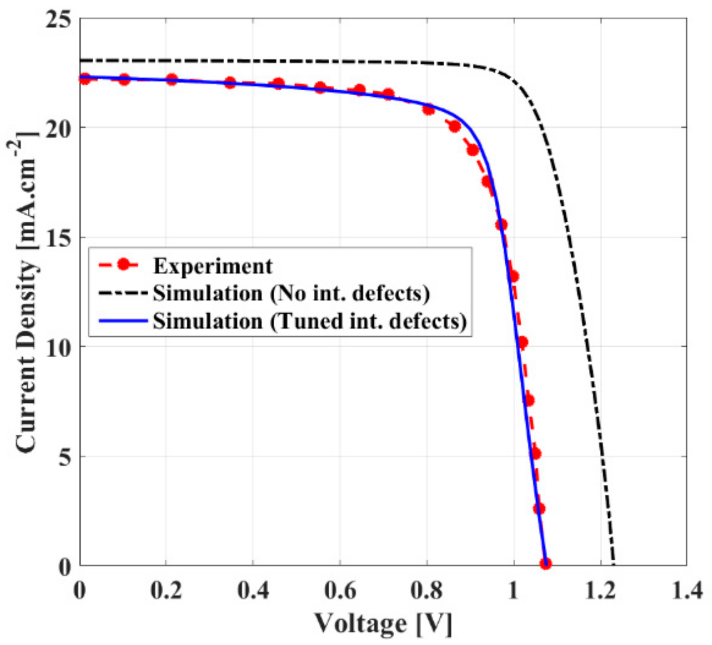
4.1. Calibration of Device Models and Parameters

The original experimental work describing the current density–voltage (J-V)characteristics is adopted from our previous published work [30]. Based on the parameters provided in Table 1 and taking the thickness of the perovskite layer to be about 500 nm, in addition to tunning some parameters such as electron (hole) mobility, and optical band gap energy, the illuminated cell can be simulated to obtain the calculated J-V curves, where the simulated characteristics were performed in the light of 1 Sun (AM 1.5G). When neglecting the interface defects, a higher performance is observed as indicated in Figure 3. The higher open-circuit voltage and short-circuit current with respect to the measured data suggest that the original cell suffers from interface defects. Now, when involving interface defects with an interface recombination velocity of 1 × 105 cm/s, a very good agreement with the experimental data was achieved as shown in Figure 3. The main optoelectronic parameters of the experimental and simulated cells are listed in Table 2. The average experimental values are recorded from a minimum of 17 cells per testing condition with a champion device PCE of 17.99% [30]. As indicated from the table, when interface defects are disabled, a PCE of 22.16% is obtained which is much higher than the experimental value as expected. On the other hand, when tuning the interface defects parameters, the simulated PCE is just 17.92% which is very near the measured value, implying the important role of interfacial traps.

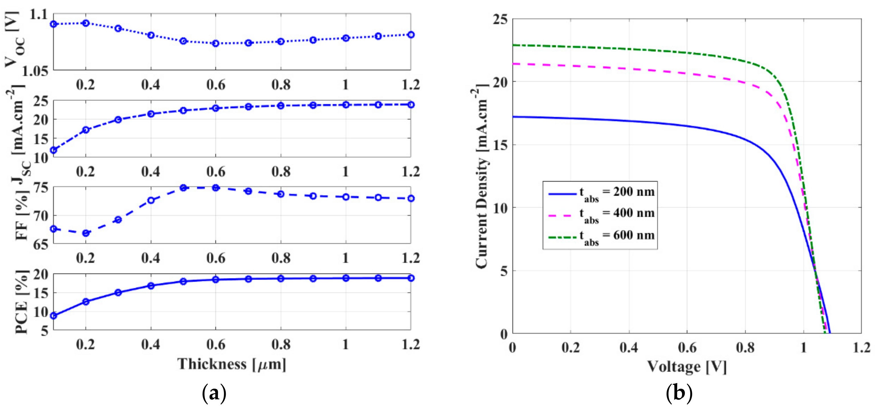
4.2. Impact of Absorber Layer Thickness

To design efficient solar cells, it is so essential to carefully choose the absorber’s layer parameters as well as the correct parameters for the ETL and HTL to maintain proper band alignment. For this purpose, we first investigated many thicknesses of the absorber layer while keeping the other parameters unaltered. The performance of the designed solar cell is tested by simulating different perovskite thicknesses ranging from 100 nm to 1200 nm. The results are shown in Figure 4a. As illustrated in Figure 4a, the variations in the Voc, Jsc, FF, and PCE were all examined as functions of absorber layer thickness. The simulated parameters revealed that the device’s Jsc increases with the increase in the absorber thickness. Note that the rise in Jsc is substantial, up to about 600 nm absorber’s thickness, after that the gain in current is almost insignificant. The PCE behaves the same as it is clear from the simulated results shown in Figure 4a that PCE increased within the mentioned range of perovskite thickness from 8.74% at 100 nm thickness up to 18.38% at 600 nm. Of course, this is expected since Jsc is the main reason for the improvement in the PCE. One notices that the increase in the PCE when the thickness exceeded 600 nm is almost negligible. This is eventually attributed to the charge carrier recombination process [58,59]. Figure 4a also shows the decreasing behavior of Voc in the range of 100 nm up to 600 nm after which Voc saturates. The reduction in the Voc values is attributed to the increase in the saturation currents caused by charge carrier recombination losses [16]. In addition, the maximum value of the FF is obtained at nearly 600 nm thickness. The simulation results suggested that the optimum thickness for the absorber can be higher than the experimental value (500 nm).
As the spectral response of the solar cell is very much dependent on the thickness of the absorber layer, the absorber thickness was further tested with the J-V profile. Figure 4b shows the J-V characteristics at varying values of the absorber thickness (200, 400, and 600 nm). One notices that Jsc increases with the thickness of the perovskite layer (17.19 mA.cm−2 at 200 nm thickness, and then reaches a saturation of 22.88 mA.cm−2 at 600 nm).

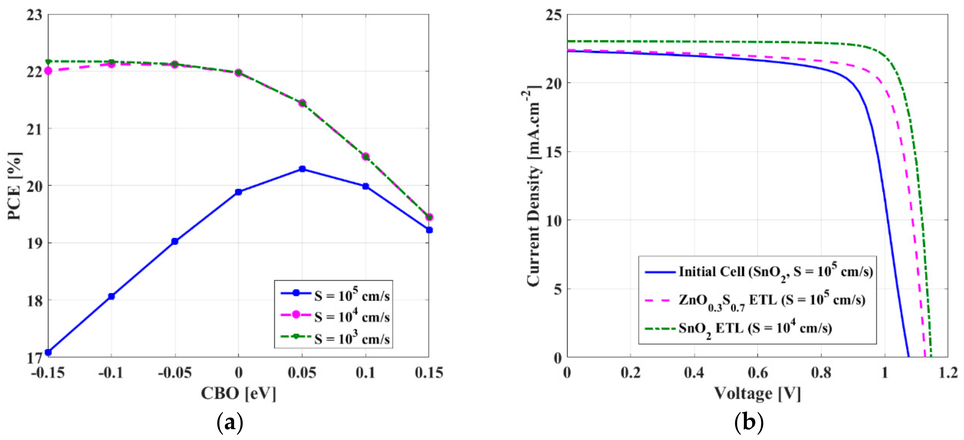
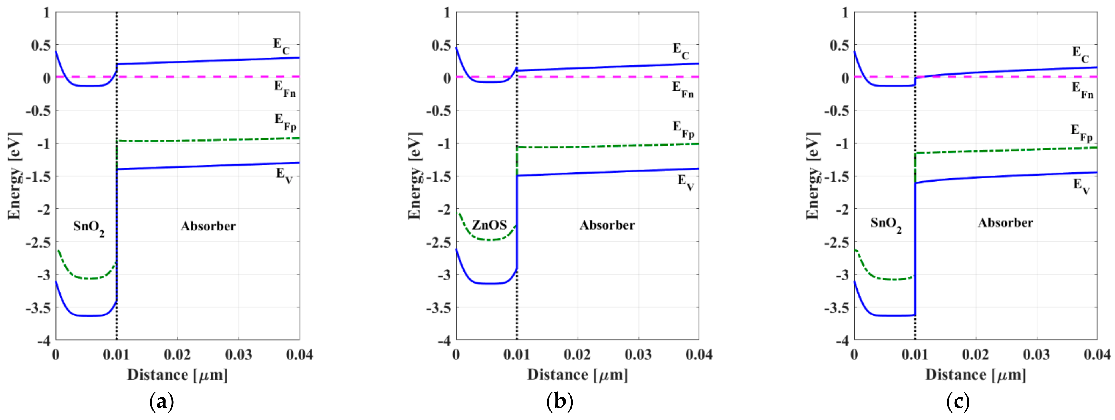
4.3. Impact of CBO and Interface Defects

To design a proper band-aligned cell, it is mandatory to engineer the conduction band offset (CBO) between the absorber layer and the ETL. The CBO is defined as the difference between the affinity of the absorber film (χabs) and that of the ETL (χETL). So, it can be formulated as:
CBO = χabs − χETL
A cliff band occurs for negative values of CBO which does not inhibit photogenerated electron transport; nonetheless, the activation energy for recombination is lower than the absorber bandgap. So, in this case, interface recombination is prevalent [60,61]. For small positive values of the CBO, a low spike band occurs which does not obstruct the transportation of carriers. In this case, the dominant recombination happens inside the absorber film instead of the interfaces [60]. However, when the spike band offset is high, the flow of carriers is blocked because of the high barrier faced at the interface.
In the following simulation, we studied the impact of the CBO on PCE while varying the surface recombination velocity at the absorber/ETL interface. Here, it is assumed that Sn = Sp = S. A variety of ETL materials along with their main physical parameters are shown in Table 3 to facilitate the selection of ETL according to the most suitable designed CBO [62,63,64,65,66]. The simulation results are displayed in Figure 5a. For S = 1 × 104 cm/s, a wide range of CBO (−0.15 to 0 eV) can achieve higher efficiencies. This range of CBO (−0.15 to 0 eV) corresponds to the range of χETL from 4.05 to 3.9 eV. So, in this case, a variety of ETL materials can be selected as suitable candidates such as WS2 and TiO2 along with SnO2 (see Table 3). On the other hand, for the higher value of S = 1 × 105 cm/s, a CBO of +0.05 eV provides the optimum choice which corresponds to χETL = 3.85 eV. So, ZnO0.3S0.7 can be a suitable candidate in this case instead of SnO2. Moreover, other choices such as WO3 and ZnO can be appropriate with a little reduction in efficiency. When S is reduced to 1×103 cm/s, the change in PCE is not significant when compared with S = 1 × 104 cm/s.
Now, the J-V curves for three cases are provided in Figure 5b. The first case is for the initial cell for which the ETL is SnO2 with a CBO of −0.1 eV. For the initial cell, S = 1 × 105 cm/s. Regarding the second case, the ETL is replaced with ZnO0.3S0.7 while keeping the same S value. Moreover, the ETL in the third case is SnO2, but with a lower S value of 1 × 104 cm/s. For the second and third cases, the obtained PCEs are 20.02% and 21.94%, respectively. A higher efficiency can be obtained when decreasing the interface recombination. Moreover, higher Voc and Jsc can be obtained for lower surface recombination although the CBO is not well-tuned. So, it is observed that improving the quality of the interface between the absorber and the ETL is more advantageous than replacing the ETL with other alternatives.
To gain a physical view of the behavior of the different studied cells, we plot the energy band diagrams of these cases under illumination. Concerning the initial cell, shown in Figure 6a, for which the CBO is −0.1 eV, the cliff band results in an activation energy for recombination of 1.5 eV which is lower than the absorber bandgap (1.6 eV), implying that the interface recombination dominates in this case. When concerning ZnO0.3S0.7, the CBO is well-designed at +0.06 eV, and a small spike band is indicated as shown in Figure 6b with an activation energy of 1.6 eV. On the other hand, for the third case, a cliff band is encountered in the initial case. However, the band bending shown in Figure 6c suggests a higher electric field than the two other cases. This high electric field, resulting from the lower surface recombination velocity, facilitates the transport of the photogenerated carriers which, in turn, enhances the performance of the cell.

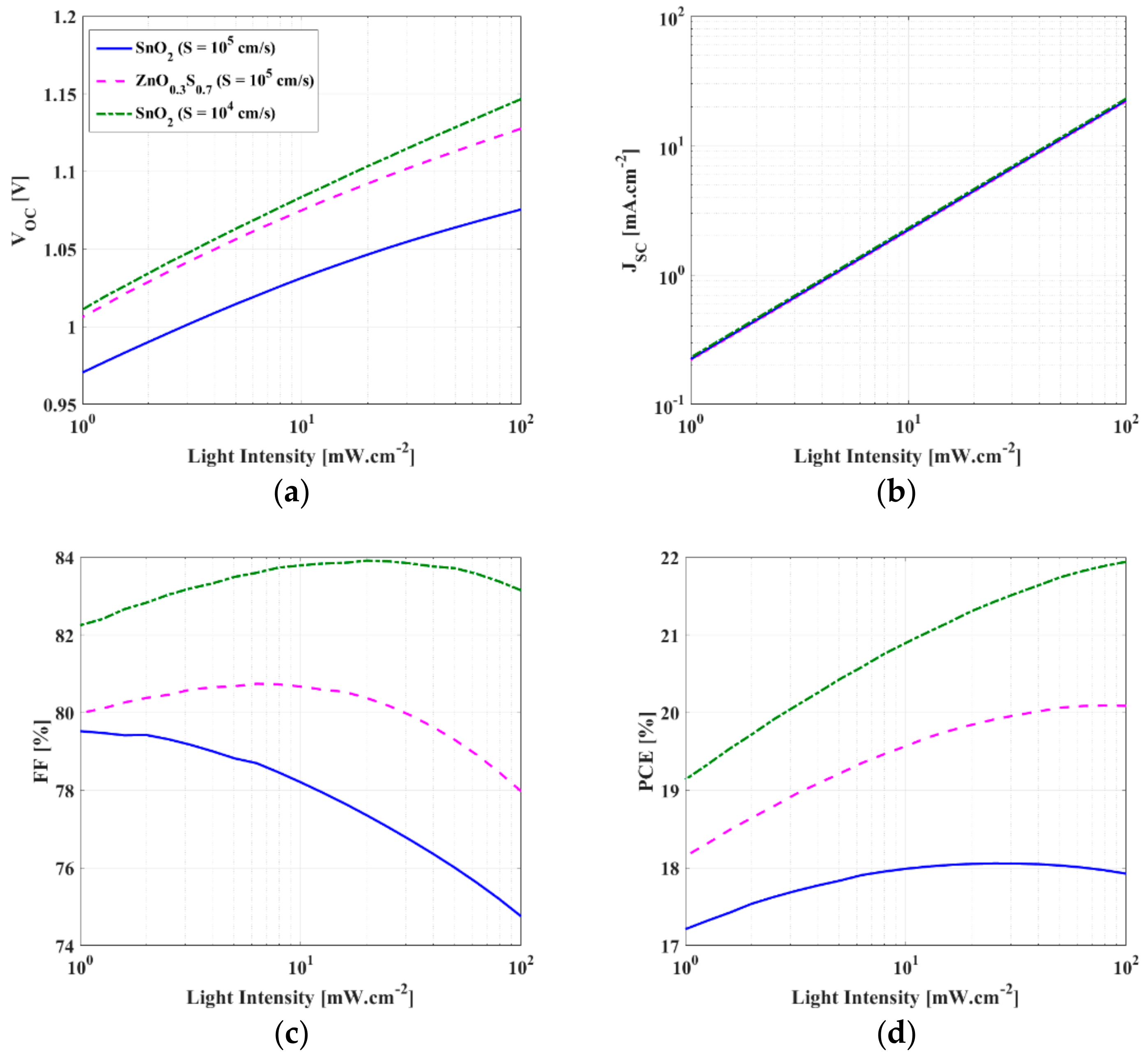
4.4. Impact of Light Intensity

In general, perovskite solar cells tested under laboratory conditions are strongly competitive candidates in photovoltaic technology. Yet, it is known that the laboratory measurements do not resemble outdoor or indoor testing since the temperature and irradiance change continuously. To obtain a clear picture of the performance of the device for more realistic conditions, a series of simulations of the device is carried out in view of light intensity change subjected to the device.
The light intensity (I) simulation part is performed at different illumination intensities in the range of 1%AM1.5G to 100%AM1.5G, where at AM 1.5 G condition, 1 sun is defined as equal to 100 mW.cm−2 of irradiance. The calculated photovoltaic parameters of the investigated cells obtained from the simulation are shown in Figure 7. The investigated cells consider (SnO2 and S = 1 × 105 cm/s), (ZnO0.3S0.7 and S = 1 × 105 cm/s), and (SnO2 and S = 1 × 104 cm/s). The simulation indicates the approximate linear trend of Voc in the semi-log scale for the three cases (see Figure 7a). The linearity of the Jsc on the log–log scale reveals that the monomolecular recombination is the dominant mechanism at short-circuit conditions for the three cell cases [67]. Further, the FF as a function of light intensity is very sensitive to the changes in interface defects as displayed in Figure 7c. Finally, the PCE variation is shown in Figure 7d. The maximum variation according to the change in intensity is observed for the optimized surface recombination case where the PCE varies from 19.14% at I = 1 mW.cm−2 to 21.94% at I = 100 mW.cm−2.

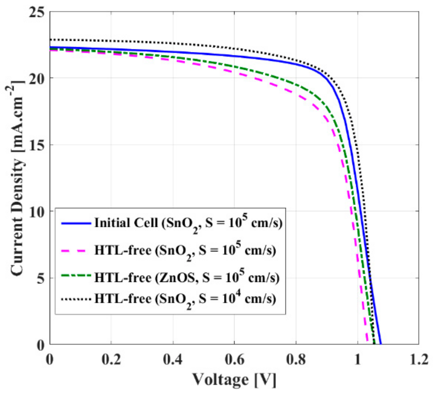
4.5. HTL-Free Design Proposal

To relieve the instability issues related to the organic HTL, we propose here to omit the HTL, so the structure is an HTL-free-based cell. It was revealed from both experimental and simulation studies that the absorber can work as an HTL in addition to its main role as a photoactive layer [68,69,70,71,72]. To test our cell performance when eliminating the HTL, we performed the simulation of three cases to investigate the effect of the HTL-free design on them. The three cells are as in the previous studies (SnO2 with S = 1 × 105 cm/s, ZnO0.3S0.7 with S = 1 × 105 cm/s, and SnO2 with S = 1 × 104 cm/s). Figure 8 shows the comparison between the three cases in terms of the illuminated J-V characteristics, while Table 4 summarizes the main performance metrics. As expected, the performance of the HTL-free is degraded when keeping SnO2 with the high value of S (giving a PCE of 15.41% instead of the initial PCE of 17.92%); however, when utilizing an appropriate CBO for the same value of S (by using ZnO0.3S0.7), it is observed that the performance is slightly deteriorated as the PCE becomes 16.14%. More interestingly, the PCE pushes to 18.28% (which is higher than the initial cell with an HTL) when reducing the surface recombination velocity to 1 × 104 cm/s. Again, the results confirm the crucial role of the interface defects for both HTL-based and HTL-free design solar cell architectures.
Finally, to provide a comparative analysis, some reported triple-cation PSC PV performance parameters along with our main work are provided in Table 5. The reported state-of-the-art solar cells are based on recent experimental studies [24,30,32,35,37,73]. All solar cells are constructed as p–i–n with organic HTLs which may have stability issues. Regarding our proposed HTL-free structure, its design can significantly improve stability. Moreover, the ETL/perovskite interface is optimized which is a crucial factor to boost cell performance. It is also noted that the interface quality in terms of the surface recombination velocity is more important to be optimized than changing the ETL material itself. Higher performance can be observed when S = 1 × 104 cm/s for SnO2 than in the case of ZnO0.3S0.7 and S = 1 × 105 cm/s. Additionally, an HTL-free design can provide a good practical stability solution, while maintaining relatively high efficiency. Remarkably, to boost the efficiency of triple-cation PSCs, more experimental work should be conducted in order to improve the quality of the interface by the appropriate design of the ETL material through engineering the CBO to minimize non-radiative recombination.

5. Conclusions

In this study, the SCAPS-1D program was utilized to investigate the optimal performance of a cesium-containing triple cation perovskite solar cell at a temperature of 300 K and standard illumination of AM1.5G. SnO2 and spiro-OMeTAD were used as the electron and hole transport layers, respectively, for the initial calibrated cell which was based on our previous experimental work. For the optimal values of input parameters and after engineering the interfacial defect properties between the ETL/absorber interface, the simulation provided Voc = 1.0755 V, Jsc = 22.297 mA.cm−2, FF = 74.75%, and PCE = 17.92% in accordance with the experimental data. The influence of absorber thickness was explored indicating a reasonable choice of 600 nm that provided the maximum PCE. In addition, investigating the significance of various values of CBO and surface recombination velocities is reflected in the enhancement of the PV device performance. Moreover, the light intensity simulation was introduced. Finally, the HTL-free design was proposed and presented. A PCE of 18.28% was obtained for the cell utilizing SnO2 as an ETL and a value of S = 1 × 104 cm/s.

Author Contributions

T.I.A. and O.I.E. had a role in the Conceptualization, Methodology, Writing—original draft, T.I.A. contributed to Validation and Investigation. O.I.E. contributed to Software, T.I.A. and O.I.E. Formal analysis, T.I.A. Resources and Writing—review and editing. All authors have read and agreed to the published version of the manuscript.

Funding

This research was funded by the Deanship of Scientific Research at Northern Border University, grant no. NR-NBU-2022-11-1568.

Data Availability Statement

Not applicable.

Acknowledgments

The authors gratefully acknowledge the approval and the support of this research study by the grant no. NR-NBU-2022-11-1568 from the Deanship of Scientific Research at Northern Border University, Arar, K.S.A.

Conflicts of Interest

The authors declare no conflict of interest.

References

  1. Zekry, A. A road map for transformation from conventional to photovoltaic energy generation and its challenges. J. King Saud Univ. Eng. Sci. 2020, 32, 407–410. [Google Scholar] [CrossRef]
  2. Okil, M.; Salem, M.S.; Abdolkader, T.M.; Shaker, A. From Crystalline to Low-cost Silicon-based Solar Cells: A Review. Silicon 2021, 14, 1895–1911. [Google Scholar] [CrossRef]
  3. Alanazi, T.I. Current Spray-Coating Approaches to Manufacture Perovskite Solar Cells. Results Phys. 2023, 44, 106144. [Google Scholar] [CrossRef]
  4. Yoshikawa, K.; Kawasaki, H.; Yoshida, W.; Irie, T.; Konishi, K.; Nakano, K.; Uto, T.; Adachi, D.; Kanematsu, M.; Uzu, H. Silicon heterojunction solar cell with interdigitated back contacts for a photoconversion efficiency Over 26%. Nat. Energy 2017, 2, 17032. [Google Scholar] [CrossRef]
  5. Zhang, Y.; Liu, H. Nanowires for High-Efficiency, Low-Cost Solar Photovoltaics. Crystals 2019, 9, 87. [Google Scholar] [CrossRef]
  6. Zhang, Y.; Fan, Z.; Zhang, W.; Ma, Q.; Jiang, Z.; Ma, D. High performance hybrid silicon micropillar solar cell based on light trapping characteristics of Cu nanoparticles. AIP Adv. 2018, 8, 055309. [Google Scholar] [CrossRef]
  7. Salem, M.S.; Alzahrani, A.J.; Ramadan, R.A.; Alanazi, A.; Shaker, A.; Abouelatta, M.; Zekry, A. Physically based analytical model of heavily doped silicon wafers based proposed solar cell microstructure. IEEE Access 2020, 8, 138898–138906. [Google Scholar] [CrossRef]
  8. Salem, M.S.; Zekry, A.; Shaker, A.; Abouelatta, M. Design and simulation of proposed low cost solar cell structures based on heavily doped silicon wafers. In Proceedings of the 2016 IEEE 43rd Photovoltaic Specialists Conference (PVSC), Portland, OR, USA, 5–10 June 2016. [Google Scholar] [CrossRef]
  9. Sun, H.; Deng, K.; Xiong, J.; Li, L. Graded bandgap perovskite with intrinsic n–p homojunction expands photon harvesting range and enables all transport layer-free perovskite solar cells. Adv. Energy Mater. 2020, 10, 1903347. [Google Scholar] [CrossRef]
  10. Gu, S.; Lin, R.; Han, Q.; Gao, Y.; Tan, H.; Zhu, J. Tin and mixed lead–tin halide perovskite solar cells: Progress and their application in tandem solar cells. Adv. Mater. 2020, 32, 1907392–1907407. [Google Scholar] [CrossRef]
  11. He, T.; Jiang, Y.; Xing, X.; Yuan, M. Structured perovskite light absorbers for efficient and stable photovoltaics. Adv. Mater. 2020, 32, 1903937–1903953. [Google Scholar] [CrossRef]
  12. Singh, A.N.; Kajal, S.; Kim, J.; Jana, A.; Kim, J.Y.; Kim, K.S. Interface engineering driven stabilization of halide perovskites against moisture, heat, and light for optoelectronic applications. Adv. Energy Mater. 2020, 10, 2000768–2000807. [Google Scholar] [CrossRef]
  13. Abdelaziz, S.; Zekry, A.; Shaker, A.; Abouelatta, M. Investigation of lead-free MASnI3-MASnIBr2 tandem solar cell: Numerical simulation. Opt. Mater. 2022, 123, 111893. [Google Scholar] [CrossRef]
  14. Salem, M.S.; Shaker, A.; Zekry, A.; Abouelatta, M.; Alanazi, A.; Alshammari, M.T.; Gontand, C. Analysis of hybrid hetero-homo junction lead-free perovskite solar cells by SCAPS simulator. Energies 2021, 14, 5741. [Google Scholar] [CrossRef]
  15. Jiang, Q.; Ni, Z.; Xu, G.; Lin, Y.; Rudd, P.N.; Xue, R.; Li, Y.; Li, Y.; Gao, Y.; Huang, J. Interfacial Molecular Doping of Metal Halide Perovskites for Highly Efficient Solar Cells. Adv. Mater. 2020, 32, e2001581. [Google Scholar] [CrossRef]
  16. Akin, S.; Arora, N.; Zakeeruddin, S.M.; Grätzel, M.; Friend, R.H.; Dar, M.I. New Strategies for Defect Passivation in High-Efficiency Perovskite Solar Cells. Adv. Energy Mater. 2020, 10, 1903090. [Google Scholar] [CrossRef]
  17. National Renewable Energy Laboratory. Best Research-Cell Efficiency Chart. Available online: https://www.nrel.gov/pv/assets/pdfs/best-research-cell-efficiencies-rev220126.pdf (accessed on 1 February 2023).
  18. Zhang, L.; Zhuang, Z.; Fang, Q.; Wang, X. Study on the Automatic Identification of ABX3 Perovskite Crystal Structure Based on the Bond-Valence Vector Sum. Materials 2023, 16, 334. [Google Scholar] [CrossRef]
  19. Min, H.; Kim, M.; Lee, S.U.; Kim, H.; Kim, G.; Choi, K.; Lee, J.H.; Seok, S.I. Efficient, stable solar cells by using inherent bandgap of α-phase formamidinium lead iodide. Science 2019, 366, 749–753. [Google Scholar] [CrossRef]
  20. Ibrahim, I.A.; Chung, C.Y. Lead-free double perovskites: How divalent cations tune the electronic structure for photovoltaic applications. J. Mater. Chem. C 2022, 10, 12276–12285. [Google Scholar] [CrossRef]
  21. Vagott, J.N.; Correa-Baena, J.-P. Multi-cation Hybrid Perovskite Solar Cells. In Hybrid Perovskite Solar Cells, 1st ed.; Fujiwara, H., Ed.; WILEY-VCH GmbH: Weinheim, Germany, 2021; pp. 339–584. [Google Scholar] [CrossRef]
  22. Jeon, N.J.; Noh, J.H.; Yang, W.S.; Kim, Y.C.; Ryu, S.; Seo, J.; Seok, S.I. Compositional engineering of perovskite materials for high-performance solar cells. Nature 2015, 517, 476–480. [Google Scholar] [CrossRef] [PubMed]
  23. Brakkee, R.; Williams, R.M. Minimizing Defect States in Lead Halide Perovskite Solar Cell Materials. Appl. Sci. 2020, 10, 3061. [Google Scholar] [CrossRef]
  24. Wang, S.; Pang, S.; Chen, D.; Zhu, W.; Xi, H.; Zhang, C. Improving perovskite solar cell performance by compositional engineering via triple-mixed cations. Sol. Energy 2021, 220, 412–417. [Google Scholar] [CrossRef]
  25. Lu, H.; Krishna, A.; Zakeeruddin, S.M.; Grätzel, M.; Hagfeldt, A. Compositional and interface engineering of organic-inorganic lead halide perovskite solar cells. iScience 2020, 23, 101359. [Google Scholar] [CrossRef]
  26. Ramasamy, E.; Suresh, K.; Mallick, S.; Rao, T.N.; Veerappan, G. Compositional engineering and surface passivation for carbon-based perovskite solar cells with superior thermal and moisture stability. J. Power Sources 2023, 559, 232645. [Google Scholar] [CrossRef]
  27. Joo, S.H.; Choi, H.W. Compositional Engineering of FAPbI3 Perovskite Added MACl with MAPbBr3 or FAPbBr3. Coatings 2021, 11, 1184. [Google Scholar] [CrossRef]
  28. Pellet, N.; Gao, P.; Gregori, G.; Yang, T.Y.; Nazeeruddin, M.K.; Maier, J.; Grätzel, M. Mixed-organic-cation Perovskite photovoltaics for enhanced solar-light harvesting. Angew. Chem. Int. Ed. 2014, 53, 3151–3157. [Google Scholar] [CrossRef] [PubMed]
  29. Yang, Z.; Chueh, C.C.; Liang, P.W.; Crump, M.; Lin, F.; Zhu, Z.; Jen, A.K.Y. Effects of formamidinium and bromide ion substitution in methylammonium lead triiodide toward high-performance perovskite solar cells. Nano Energy 2016, 22, 328–337. [Google Scholar] [CrossRef]
  30. Alanazi, T.I.; Game, O.S.; Smith, J.A.; Kilbride, R.C.; Greenland, C.; Jayaprakash, R.; Georgiou, K.; Terrill, N.J.; Lidzey, D.G. Potassium iodide reduces the stability of triple-cation perovskite solar cells. RSC Adv. 2020, 10, 40341–40350. [Google Scholar] [CrossRef]
  31. Montoya, D.M.; Pérez-Gutiérrez, E.; Barbosa-Garcia, O.; Bernal, W.; Maldonado, J.L.; Percino, M.J.; Meneses, M.A.; Cerón, M. Defects at the interface electron transport layer and alternative counter electrode, their impact on perovskite solar cells performance. Sol. Energy 2020, 195, 610–617. [Google Scholar] [CrossRef]
  32. Cao, Y.; Liu, H.; Gao, F.; Li, D.; Xiang, L.; Gao, J.; Gao, P.; Zhang, Y.; Li, S. Interface Optimization and Growth Control for High Efficiency Wide Bandgap Perovskite Solar Cells. Surf. Interfaces 2023, 37, 102680. [Google Scholar] [CrossRef]
  33. Sun, H.; Xie, D.; Song, Z.; Liang, C.; Xu, L.; Qu, X.; Yao, Y.; Li, D.; Zhai, H.; Zheng, K.; et al. Interface defects passivation and conductivity improvement in planar perovskite solar cells using Na2S-doped compact TiO2 electron transport layers. ACS Appl. Mater. Interfaces 2020, 12, 22853–22861. [Google Scholar] [CrossRef] [PubMed]
  34. Zhang, B.; Su, J.; Guo, X.; Zhou, L.; Lin, Z.; Feng, L.; Zhang, J.; Chang, J.; Hao, Y. NiO/perovskite heterojunction contact engineering for highly efficient and stable perovskite solar cells. Adv. Sci. 2020, 7, 1903044. [Google Scholar] [CrossRef]
  35. Zanetta, A.; Bulfaro, I.; Faini, F.; Manzi, M.; Pica, G.; De Bastiani, M.; Bellani, S.; Zappia, M.I.; Bianca, G.; Gabatel, L.; et al. Enhancing charge extraction in inverted perovskite solar cells contacts via ultrathin graphene: Fullerene composite interlayers. J. Mater. Chem. A 2023. [Google Scholar] [CrossRef]
  36. Chen, Y.; Yang, J.; Wang, S.; Wu, Y.; Yuan, N.; Zhang, W.H. Interfacial contact passivation for efficient and stable cesium-formamidinium double-cation lead halide perovskite solar cells. iScience 2020, 23, 100762. [Google Scholar] [CrossRef]
  37. Malouangou, M.D.; Zhang, Y.; Yang, Y.; Mbumba, M.T.; Akram, M.W.; Rop, E.; Matondo, J.T.; Guli, M. Enhancing the efficiency and stability of 2D-3D perovskite solar cells with embedded interface passivation with diammonium cation spacer. Sol. Energy Mater. Sol. Cells 2023, 251, 112135. [Google Scholar] [CrossRef]
  38. Wang, C.; Liu, M.; Rahman, S.; Pasanen, H.P.; Tian, J.; Li, J.; Deng, Z.; Zhang, H.; Vivo, P. Hydrogen bonding drives the self-assembling of carbazole-based hole-transport material for enhanced efficiency and stability of perovskite solar cells. Nano Energy 2022, 101, 107604. [Google Scholar] [CrossRef]
  39. Xu, Y.; Liu, F.; Li, R.; Jing, Y.; Chen, Q.; Chen, X.; Deng, C.; Du, Z.; Sun, W.; Wu, J.; et al. MXene regulates the stress of perovskite and improves interface contact for high-efficiency carbon-based all-inorganic solar cells. Chem. Eng. J. 2023, 461, 141895. [Google Scholar] [CrossRef]
  40. Chowdhury, T.A.; Zafar, M.A.B.; Islam, M.S.U.; Shahinuzzaman, M.; Islam, M.A.; Khandaker, M.U. Stability of perovskite solar cells: Issues and prospects. RSC Adv. 2023, 13, 1787–1810. [Google Scholar] [CrossRef] [PubMed]
  41. Alam, I.; Ashraf, M.A. Effect of different device parameters on tin-based perovskite solar cell coupled with In2S3 electron transport layer and CuSCN and Spiro-OMeTAD alternative hole transport layers for high-efficiency performance. Energy Sources Part A Recovery Util. Environ. Eff. 2020, 1–25. [Google Scholar] [CrossRef]
  42. Coulibaly, A.B.; Oyedele, S.O.; Kre, N.R.; Aka, B. Comparative Study of Lead-Free Perovskite Solar Cells Using Different Hole Transporter Materials. Model. Numer. Simul. Mater. Sci. 2019, 9, 97–107. [Google Scholar] [CrossRef]
  43. Gamal, N.; Sedky, S.H.; Shaker, A.; Fedawy, M. Design of Lead-Free Perovskite Solar Cell using Zn1-xMgxO as ETL: SCAPS Device Simulation. Optik 2021, 242, 167306. [Google Scholar] [CrossRef]
  44. Alanazi, T.I. Design and Device Numerical Analysis of Lead-Free Cs2AgBiBr6 Double Perovskite Solar Cell. Crystals 2023, 13, 267. [Google Scholar] [CrossRef]
  45. Basyoni, M.S.S.; Salah, M.M.; Mousa, M.; Shaker, A.; Zekry, A.; Abouelatta, M.; Alshammari, M.T.; Al-Dhlan, K.A.; Gontrand, C. On the Investigation of Interface Defects of Solar Cells: Lead-Based vs Lead-Free Perovskite. IEEE Access 2021, 9, 130221–130232. [Google Scholar] [CrossRef]
  46. Prasanna, J.L.; Goel, E.; Kumar, A.; Laref, A.; Santhosh, C.; Ranjan, P.; Kumar, A. Bandgap graded perovskite solar cell for above 30% efficiency. Optik 2022, 269, 169891. [Google Scholar] [CrossRef]
  47. Sinha, N.K.; Roy, P.; Ghosh, D.S.; Khare, A. Simulation and analysis of Schottky junction perovskite solar cells (SJPSCs). In Proceedings of the IOP Conference Series: Materials Science and Engineering, Raipur, India, 28–29 December 2020; IOP Publishing: Bristol, UK, 2021; Volume 1120, p. 012017. [Google Scholar]
  48. Burgelman, M.; Decock, K.; Niemegeers, A.; Verschraegen, J.; Degrave, S. SCAPS Manual; University of Gent: Ghent, Belgium, 2014. [Google Scholar]
  49. Shockley, W.T.R.W.; Read, W.T., Jr. Statistics of the recombinations of holes and electrons. Phys. Rev. 1952, 87, 835. [Google Scholar] [CrossRef]
  50. Pauwels, H.J.; Vanhoutte, G. The influence of interface state and energy barriers on the efficiency of heterojunction solar cells. J. Phys. D Appl. Phys. 1978, 11, 649–667. [Google Scholar] [CrossRef]
  51. Ye, M.; He, C.; Iocozzia, J.; Liu, X.; Cui, X.; Meng, X.; Rager, M.; Hong, X.; Liu, X.; Lin, Z. Recent advances in interfacial engineering of perovskite solar cells. J. Phys. D Appl. Phys. 2017, 50, 373002. [Google Scholar] [CrossRef]
  52. Patel, P.K. Device simulation of highly efficient eco-friendly CH3NH3SnI3 perovskite solar cell. Sci. Rep. 2021, 11, 3082. [Google Scholar] [CrossRef]
  53. Mohandes, A.; Moradi, M.; Nadgaran, H. Numerical simulation of inorganic Cs2AgBiBr6 as a lead-free perovskite using device simulation SCAPS-1D. Opt. Quantum Electron. 2021, 53, 319. [Google Scholar] [CrossRef]
  54. Alkhammash, H.I.; Mottakin, M.; Hossen, M.M.; Akhtaruzzaman, M.; Rashid, M.J. Design and defect study of Cs2AgBiBr6 double perovskite solar cell using suitable charge transport layers. Semicond. Sci. Technol. 2022, 38, 015005. [Google Scholar] [CrossRef]
  55. Prathapani, S.; Bhargava, P.; Mallick, S. Electronic band structure and carrier concentration of formamidinium–cesium mixed cation lead mixed halide hybrid perovskites. Appl. Phys. Lett. 2018, 112, 092104. [Google Scholar] [CrossRef]
  56. Karthick, S.; Velumani, S.; Bouclé, J. Experimental and SCAPS simulated formamidinium perovskite solar cells: A comparison of device performance. Sol. Energy 2020, 205, 349–357. [Google Scholar] [CrossRef]
  57. Abena, A.N.; Ngoupo, A.T.; Ndjaka, J.M.B. Computational analysis of mixed cation mixed halide-based perovskite solar cell using SCAPS-1D software. Heliyon 2022, 8, e11428. [Google Scholar] [CrossRef]
  58. Saikia, D.; Bera, J.; Betal, A.; Sahu, S. Performance evaluation of an all inorganic CsGeI3 based perovskite solar cell by numerical simulation. Opt. Mater. 2022, 123, 111839. [Google Scholar] [CrossRef]
  59. Sahli, F.; Werner, J.; Kamino, B.A.; Bräuninger, M.; Yang, T.C.J.; Fiala, P.; Nogay, G.; Fu, F.; Monnard, R.; Walter, A.; et al. Hybrid sequential deposition process for fully textured perovskite/silicon tandem solar cells. In Proceedings of the 2018 IEEE 7th World Conference on Photovoltaic Energy Conversion, WCPEC 2018-A Joint Conference of 45th IEEE PVSC, 28th PVSEC and 34th EU PVSEC, Waikoloa, HI, USA, 10–15 June 2018; pp. 3571–3574. [Google Scholar] [CrossRef]
  60. Minemoto, T.; Murata, M. Theoretical analysis on effect of band offsets in perovskite solar cells. Sol. Energy Mater. Sol. Cells 2015, 133, 8–14. [Google Scholar] [CrossRef]
  61. Tanaka, K.; Minemoto, T.; Takakura, H. Analysis of hetero interface recombination by Zn1-xMgxO for window layer of Cu(In,Ga)Se2 solar cells. Sol. Energy 2009, 83, 477–479. [Google Scholar] [CrossRef]
  62. Li, K.; Kondrotas, R.; Chen, C.; Lu, S.; Wen, X.; Li, D.; Luo, J.; Zhao, Y.; Tang, J. Improved efficiency by insertion of Zn1−xMgxO through sol-gel method in ZnO/Sb2Se3 solar cell. Sol. Energy 2018, 167, 10–17. [Google Scholar] [CrossRef]
  63. Rai, N.; Rai, S.; Singh, P.K.; Lohia, P.; Dwivedi, D.K. Analysis of various ETL materials for an efficient perovskite solar cell by numerical simulation. J. Mater. Sci. Mater. Electron. 2020, 31, 16269–16280. [Google Scholar] [CrossRef]
  64. Gharibshahian, I.; Orouji, A.A.; Sharbati, S. Efficient Sb2(S, Se)3/Zn (O, S) solar cells with high open-circuit voltage by controlling sulfur content in the absorber-buffer layers. Sol. Energy 2021, 227, 606–615. [Google Scholar] [CrossRef]
  65. Zhang, Y.; Blom, P.W. Electron and hole transport in poly (fluorene-benzothiadiazole). Appl. Phys. Lett. 2011, 98, 143504. [Google Scholar] [CrossRef]
  66. Hossain, M.K.; Rubel, M.H.K.; Toki, G.I.; Alam, I.; Rahman, M.F.; Bencherif, H. Effect of various electron and hole transport layers on the performance of CsPbI3-based perovskite solar cells: A numerical investigation in DFT, SCAPS-1D, and wxAMPS frameworks. ACS Omega 2022, 7, 43210–43230. [Google Scholar] [CrossRef]
  67. Yin, Z.; Wei, J.; Zheng, Q. Interfacial Materials for Organic Solar Cells: Recent Advances and Perspectives. Adv. Sci. 2016, 3, 1500362. [Google Scholar] [CrossRef] [PubMed]
  68. Behrouznejad, F.; Shahbazi, S.; Taghavinia, N.; Wu, H.P.; Diau, E.W.G. A study on utilizing different metals as the back contact of CH3NH3PbI3 perovskite solar cells. J. Mater. Chem. A 2016, 4, 13488–13498. [Google Scholar] [CrossRef]
  69. Chu, Q.Q.; Ding, B.; Li, Y.; Gao, L.L.; Qiu, Q.; Li, C.X.; Li, C.J.; Yang, G.J.; Fang, B. Fast drying boosted performance improvement of low-temperature paintable carbon-based perovskite solar cell. ACS Sustain. Chem. Eng. 2017, 5, 9758–9765. [Google Scholar] [CrossRef]
  70. Pradid, P.; Sanglee, K.; Thongprong, N.; Chuangchote, S. Carbon Electrodes in Perovskite Photovoltaics. Materials 2021, 14, 5989. [Google Scholar] [CrossRef]
  71. Chakraborty, D.; Somay, S.; Pandey, S.K. Numerical analysis of a novel HTL-free perovskite solar cell with gradient doping and a WS₂ interlayer. Micro Nanostruct. 2022, 163, 107149. [Google Scholar] [CrossRef]
  72. Sunny, A.; Rahman, S.; Khatun, M.M.; Ahmed, S.R.A. Numerical study of high performance HTL-free CH3NH3SnI3-based perovskite solar cell by SCAPS-1D. AIP Adv. 2021, 11, 065102. [Google Scholar] [CrossRef]
  73. Kadhim, M.J.; Mohammed, M.K. Fabrication of efficient triple-cation perovskite solar cells employing ethyl acetate as an environmental-friendly solvent additive. Mater. Res. Bull. 2023, 158, 112047. [Google Scholar] [CrossRef]
Figure 1. A simplified flowchart representing the simulation procedure, inputs and outputs of the SCAPS-1D simulator.
Energies 16 02717 g001
Figure 2. (a) Schematic representation of the planer structure of the triple-cation perovskite solar cell with configuration ITO/SnO2/perovskite/Spiro-OMeTAD/Au showing the various thicknesses of the basic layers, (b) a cross-section SEM image of TCPCS (reproduced from Ref. [30] with permission from the Royal Society of Chemistry), and (c) energy band diagram at dark condition and zero bias.
Energies 16 02717 g002
Figure 3. J-V for experimental work and simulation for two cases: without interface defects and with tuned interface defects to fit the experimental data.
Energies 16 02717 g003
Figure 4. (a) Variations in open-circuit voltage, short-circuit current, fill factor, and PCE of the device as a function of the absorber layer thickness and (b) J-V curves of the device simulated with three different values of the absorber thickness.
Energies 16 02717 g004
Figure 5. (a) Impact of CBO on PCE for three different values of surface recombination velocities. (b) J-V characteristics for initial, ZnOS, and SnO2 cells.
Energies 16 02717 g005
Figure 6. Energy band diagrams under illumination for (a) initial cell (SnO2 and S = 105 cm/s), (b) modified CBO cell (ZnO0.3S0.7 and S = 105 cm/s) and (c) modified S cell (SnO2 and S = 104 cm/s).
Energies 16 02717 g006
Figure 7. PV parameters of triple-cation perovskite solar cell at various light intensities (a) Voc, (b) Jsc, (c) FF, and (d) PCE.
Energies 16 02717 g007
Figure 8. Comparison of J-V curves for various HTL-free design case studies vs. initial cell.
Energies 16 02717 g008
Table 1. Physical parameters used in simulations for each layer of the device.
Material PropertiesSpiro-OMeTAD
[30,53,54]
TC Perovskite
[30,55,56]
SnO2
[30,57]
εr3.066.69
χ (eV)2.23.94.0
Eg (eV)2.91.63.5
µn/p (cm2 V−1 s−1)2 × 10⁻⁴/2 × 10−42.0/2.020/10
NA (cm−3)2 × 101910150
ND (cm−3)002.2 × 10¹⁷
NC (cm−3)2.2 × 101810182.2 × 1016
NV (cm−3)1.9 × 101910181019
Table 2. Comparative evaluation of the model performance parameters’ values with experimental and simulated values at room temperature.
Experimental Data [30]Simulation
(No Interface Defects)
Simulation
(Tuned Interface Defects)
Voc (V)1.08 ± 0.011.23131.0755
Jsc (mA.cm−2)22.33 ± 0.4123.04122.297
FF (%)75.68 ± 1.3278.1374.75
PCE (%)17.51 ± 0.4822.1617.92
Table 3. Physical parameters of some ETL candidates.
Zn0.85Mg0.15O
[62]
WO3
[63]
ZnO0.3S0.7
[64]
ZnO
[63]
WS2
[65]
TiO2
[66]
Eg (eV)3.552.63.073.31.83.2
χ (eV)3.753.83.843.93.954
CBO (eV)+0.15+0.1+0.060−0.05−0.1
εr9.04.89.09.013.69.0
µn/p (cm2/Vs)50/2030/30100/2550/5100/10020/10
Nc (cm−3)9 × 10162.2 × 10212.2 × 10181.0 × 10192.2 × 10172 × 1018
Nv (cm−3)9 × 10172.2 × 10211.8 × 10181.0 × 10192.2 × 10161.8 × 1019
Table 4. Comparative evaluation of the HTL-based and HTL-free simulated design.
Initial CellHTL-Free
(SnO2 ETL)
HTL-Free
(ZnOS ETL)
HTL-Free
(SnO2 ETL)
S (cm/s)1 × 1051 × 1051 × 1051 × 104
Voc (V)1.07551.03331.0551.054
Jsc (mA.cm−2)22.29722.08522.16722.861
FF (%)74.7567.5168.9975.84
PCE (%)17.9215.4116.1418.28
Table 5. State-of-the-art comparison between typical PV performance of triple-cation PSCs reported in the literature and our work.
Triple-Cation PerovskiteVoc
(V)
Jsc
(mA.cm−2)
FF (%)PCE (%)REF
Guay(FAMA)1-yPbIxCl3-x1.1423.8078.0021.30[24]
FA0.8Cs0.16MA0.04Pb(I0.5Br0.5)31.2217.6473.0015.70[32]
Cs0.05FA0.79MA0.16Pb(I0.90Br0.10)31.09822.4085.0020.80[35]
Cs0.05(FA0.83MA0.17)0.95Pb(I0.83Br0.17)31.14523.7877.8921.15[37]
Cs(MAFA)Pb(IBr)31.05422.1679.7818.63[73]
Cs0.05FA0.79MA0.15PbI2.45Br0.55
(ZnO0.3S0.7 and S = 1 × 105 cm/s)
1.12821.7078.8320.09This work
Cs0.05FA0.79MA0.15PbI2.45Br0.55
(SnO2 and S = 1 × 104 cm/s)
1.14723.0283.1521.94This work
Cs0.05FA0.79MA0.15PbI2.45Br0.55
(HTL-free cell)
1.054022.86175.8418.28This work
Disclaimer/Publisher’s Note: The statements, opinions and data contained in all publications are solely those of the individual author(s) and contributor(s) and not of MDPI and/or the editor(s). MDPI and/or the editor(s) disclaim responsibility for any injury to people or property resulting from any ideas, methods, instructions or products referred to in the content.

