Article

Investigating the Performance of Efficient and Stable Planer Perovskite Solar Cell with an Effective Inorganic Carrier Transport Layer Using SCAPS-1D Simulation

1
Institute of Microelectronics of Chinese Academy of Sciences, Beijing 100029, China
2
University of Chinese Academy of Sciences, Beijing 100049, China
3
University of Science and Technology of China, Hefei 230026, China
4
Suzhou Institute for Advanced Research, University of Science and Technology of China, Suzhou 215123, China
*
Authors to whom correspondence should be addressed.
Energies 2023, 16(21), 7438; https://doi.org/10.3390/en16217438
Submission received: 24 September 2023 / Revised: 19 October 2023 / Accepted: 24 October 2023 / Published: 3 November 2023

Abstract

:
Organic–inorganic metal halide perovskite (OIMHP) has emerged as a promising material for solar cell application due to their outstanding optoelectronics properties. The perovskite-based solar cell (PSC) demonstrates a significant enhancement in efficiency of more than 20%, with a certified efficiency rating of 23.13%. Considering both the Shockley limit and bandgap, there exists a substantial potential for further efficiency improvement. However, stability remains a significant obstacle in the commercialization of these devices. Compared to organic carrier transport layers (CTLs), inorganic material such as ZnO, TiO2, SnO2, and NiOX offer the advantage of being deposited using atomic layer deposition (ALD), which in turn improves the efficiency and stability of the device. In this study, methylammonium lead iodide (MAPbI3)-based cells with inorganic CTL layers of SnO2 and NiOX are simulated using SCAPS-1D software. The cell structure configuration comprises ITO/SnO2/CH3NH3PbI3/NiOX/Back contact where SnO2 and NiOX act as ETL and HTL, respectively, while ITO is a transparent front-end electrode. Detailed investigation is carried out into the influence of various factors, including MAPbI3 layer size, the thickness of CTLs, operating temperature parasitic resistance, light intensity, bulk defects, and interfacial defects on the performance parameters. We found that the defects in layers and interface junctions greatly influence the performance parameter of the cell, which is eliminated through an ALD deposition approach. The optimum size of the MAPbI3 layer and CTL was found to be 400 nm and 50 nm, respectively. At the optimized configuration, the PSC demonstrates an efficiency of 22.13%, short circuit current (JSC) of 20.93 mA/m2, open circuit voltage (VOC) of 1.32 V, and fill factor (FF) of 70.86%.

1. Introduction

The PSC has recently received a lot of attention due to a significant increase in power conversion efficiency (PCE) and advancements in design and manufacturing techniques [1]. According to the NREL cell efficiency chart, the efficiency of PSC has reached 26%. In the last six years, PSC efficiency has increased by 2.27% per year from the first developed PSC of 9.7%, which has greatly surpassed other kinds of solar cells, which have increased by less than 1.0% per year [2]. PCE advancements were made possible by scientific knowledge as well as engineering advancements. The former refers to the crystal formation, composition alteration, and optoelectronics capabilities, while the latter refers to interfacial changing and the formation of highly efficient carrier transportation layers (CTLs). CTLS are subdivided into electron and hole transport layers (ETLs and HTLs) [2].
The fundamental design of PSC consists of perovskite material sandwiched between the ETL and HTL in NIP or PIN configuration. Under solar illumination, the light interacts with a PSC structure from the upper side through the glass substrate coated with transparent electrodes such as tin-doped indium oxide, HTL, or ETL, which is finally absorbed by the perovskite layer and photo-generated electron-hole pairs are created. In this process, there are several possibilities for the incident photon, for example, the photon might be reflected or scattered and will not contribute to the photo-current of the PSC [3]. One strategy is to apply an antireflection coating to reduce photon losses on the glass substrate. However, it will eventually increase the PSC production cost [4].
The ETL transport electron, utilizing n-type material and its conduction band minimum (CBM), should be smaller than the perovskite material. The HTL requires p-type materials with a higher valance band maximum (VBM) than the perovskite material.
The main obstacles in commercializing PSCs are their stability (life span). They are more sensitive to external stimuli such as light, heat, oxygen, and water. PSCs exposed to such conditions can cause rapid degradation of the cell structure that in turn causes cell failure, leaving harmful effect on the biological environment by releasing toxic elements such as Pb ions [5].
The performance is further reduced because of the inappropriate selection of ETLs and HTLs. Most commonly used PSCs in NIP configurations use TiO2 as the ETL, while Spiro-OMeTAD is employed as the HTL and in PIN, PEDOT: PSS, and PTAA are used as HTL. TiO2 shows poor stability against ultraviolet (UV) radiation and needs additional layers to screen the UV rays. Spiro-OMeTAD shows inadequate thermal and air stability, while PEDOT: PSS did not sustain its stability for a long time due to its acidic and hygroscopic properties [6,7,8].
Compared to organic, inorganic CTL-based PSCs have been recently developed which display excellent properties. Some inorganic material used for ETLs include SnO2, TiO2, ZnO, BaSnO3, and Zn2SnO4, and those used for HTL include NiOX, CuI, MoO3, CrOx, and CuOX [2].
Another significant factor that enhanced the efficiency and stability of PSC is the deposition technique. Compare to other deposition techniques, ALD is an excellent tool to deposit defect-free thin-films with higher accuracy and conformity. The PSC fabrication, which includes the deposition of ETL and HTL layers, passivation or interference layers, and encapsulation of the device can be easily achieved with ALD tools, and can be considered an upgrade in cell performance [2,9,10]. It is important to decrease the series resistances and increase the shunt resistance, which is associated with the thickness and quality of the CTLs and perovskite layers [11]. The ordinary thin-films containing cracks and pinholes that provide pathways to shunt leakage current that can badly affect the cell’s performance. In contrast, thickening CTL layers can increase the series resistance, which drops the output voltage [12,13]. In this scenario, ALDs can provide an excellent CTL layer, having uniform and dense film formation along with accurate control in the sub-nanometer range.
Similarly, in PSC, the interference between perovskite and CTL layers are the main source of electron-hole recombination (losses) which directly affect the efficiency of PV cells. The surface passivation technique is used to deposit ultra-thin layer at low temperatures at the surface to avoid thermally generated crakes and pinholes in the layers [14]. ALDs have been widely adopted as a solution in the P.V. industry to provide high-quality, low-temperature, and uniform passivation layers. With the help of the passivation layer, it not only improves cell efficiency, but also increases the stability of PSCs by protecting them from environmental hazard conditions.
Numerical simulation is the best theoretical approach to predict the solar cell performance before developing a prototype. SCAPS-1D is widely utilized in research on solar cells, including PSC, to examine the performance parameters. Hossain et al. [15] simulated lead-free Sc3Bi2I9-based PSCs using SCAPS for 49 different configurations, and found that Cu2O is a cost-effective and efficient HTL layer for lead-free PSC. Saha et al. [16] simulated (SCAPS-1D) MaPbI3-based PSCs with grapheme-doped TiO2 ETLs and PTAA as HTLs recorded an efficiency of 22.7%. Mushtaq et al. [17] developed PSC having a configuration FTO/SnO2/MASnBr3/NiO/Au demonstrating the potential of MASnBr3, an eco-economical, high-performance, and removable energy solution. Hussain et al. [18] investigated lead-free CH3NH3SnI3 with SnO2 and Spiro-OMeTAD recorded an efficiency of 33.26%. Sunny et al. [19] developed a SCAPS model of HTL-free PSCs using CH3NH3SnI3 and TiO2 ETL and the optimized structure achieved a 6.33% efficiency, making it a cost-effective and efficient PSC. Ibrahim et al. [20] investigated the effect defect in the absorber and ETL/perovskite interference of PSCs using SCAPS tool. The result shows that varying defect density from 1010 cm−3 to 1018 cm−3 causes significant drops in the performance parameter of the cell. Samiul Islam et al. [21] study lead-free CH3NH3SnBr3-based PSCs. The model explores the effects of defects, parasitic resistance, and work functions of the contact. Similarly, Basyoni et al. [22] investigated interference defects between CTLs with lead- and lead-free PSCs to optimize the performance using a SCAPS simulator. It reveals that defects play a crucial role in increasing the efficiency of lead-free PSCs from 1.76% to 5.35%, highlighting the importance of interface engineering in PSC design. In this study, we will explore the performance of PSCs using inorganic CTL materials that can be easily deposited with ALD, such as ZnO, TiO2, SnO2, and NiOX, utilizing the SCAPS tool. These materials have the benefit of being deposited using ALD processes, which improves the device’s efficiency and stability.
The NiOX is a favorable HTL material used for several photovoltaic (P.V) application due to its intrinsic p-type semiconductor nature, superior hole extraction property, low processing temperature, good optical properties, low-cost, and good chemical and thermal stability [23,24,25].
Similarly, SnO2-based PSC efficiency is recorded up to 25%, making SnO2 to be a good ETL choice in PSCs, and a potential substitute for TiO2 [26,27]. The SnO2 has extraordinary properties which are required for efficient and stable PSCs, including high-bulk electron mobility and conductivity [28,29], high temperature flexible deposition, large bandgap (3.6–4.5 eV), high optical transparency, and excellent stability under heat, moisture, and light with negligible photo-activity [30,31]. Compared to TiO2, SnO2 ETL requires less temperature (<200 °C) when using chemical bath deposition or spin coating, which is an advantage when it comes to mass production. However, there are certain flaws in the hetero interference that degrade the performance of PSCs due to the mismanagement of the perovskite film and metal oxide. Therefore, the passivation layer of Al2O3 on the SnO2 layer is used to upgrade the performance of SnO2-based PSCs [32]. In addition to this, NiOX and SnO2 material show negligible hysteresis behaviors that will help to disclose the actual performance of the PSC.

2. SCAPS Simulation

The numerical simulation is the best and easiest approach to comprehend the fundamental operation of the solar cell, revealing the factors that influence their functionality. This investigation was carried out with the help of the SCAPS-1D (solar cell capacitance simulator) software application. SCAPS-1D was developed by Marc Burgelman at the University of Gent, solving thin-film structures in one dimension using electrical and optical parameters [33]. This simulation tool utilizes well-known semiconductor equations such as Poisson’s equation, continuity equation, and transport equation to solve the solar cell model and provide parameter measurements of the designed PV cell. The Poisson’s equation is used to obtain internal potential distribution within the cell. The continuity equation describes the rate of change in the concentration of carriers (electrons and holes). The transport equation provides information of how the electrons and hole travels in the cell structure. Once the cell structure is defined, the SCAPS solve the following equation from (1)–(5) providing the performance capability of the device.
2 x 2 φ x = q ε n x p x
n , p t = 1 q J n x + G x R n + 1 q J p x + ( G x R p )
J n , p = q µ n n E + q D n n x + q µ p p E + q D p p x
D n . p = K b T q µ n , p   and   L n , p = D τ
V O C = V T ln I l i g h t I o + 1
where ε is permittivity, q is the elementary charge, φ x stands for electrostatic potential, n and p are electron and hole density, E is the electric field, D n and D p are the diffusion coefficient, and µ n and µ p are carriers’ mobility. The expression of diffusivity in Equation (4) refers to the ability of carriers to scatters or spread out within the materials where the diffusion length L n , p indicates the distance traveled by the carriers between the generation and recombination period. When no external load is applied, the terminal voltage is considered open circuit voltage (VOC) given by Equation (5). Similarly, when the terminal of the solar cell is short circuited with each other, (VOC become zero) it provides a reading of the short circuit current or the light-generated current.

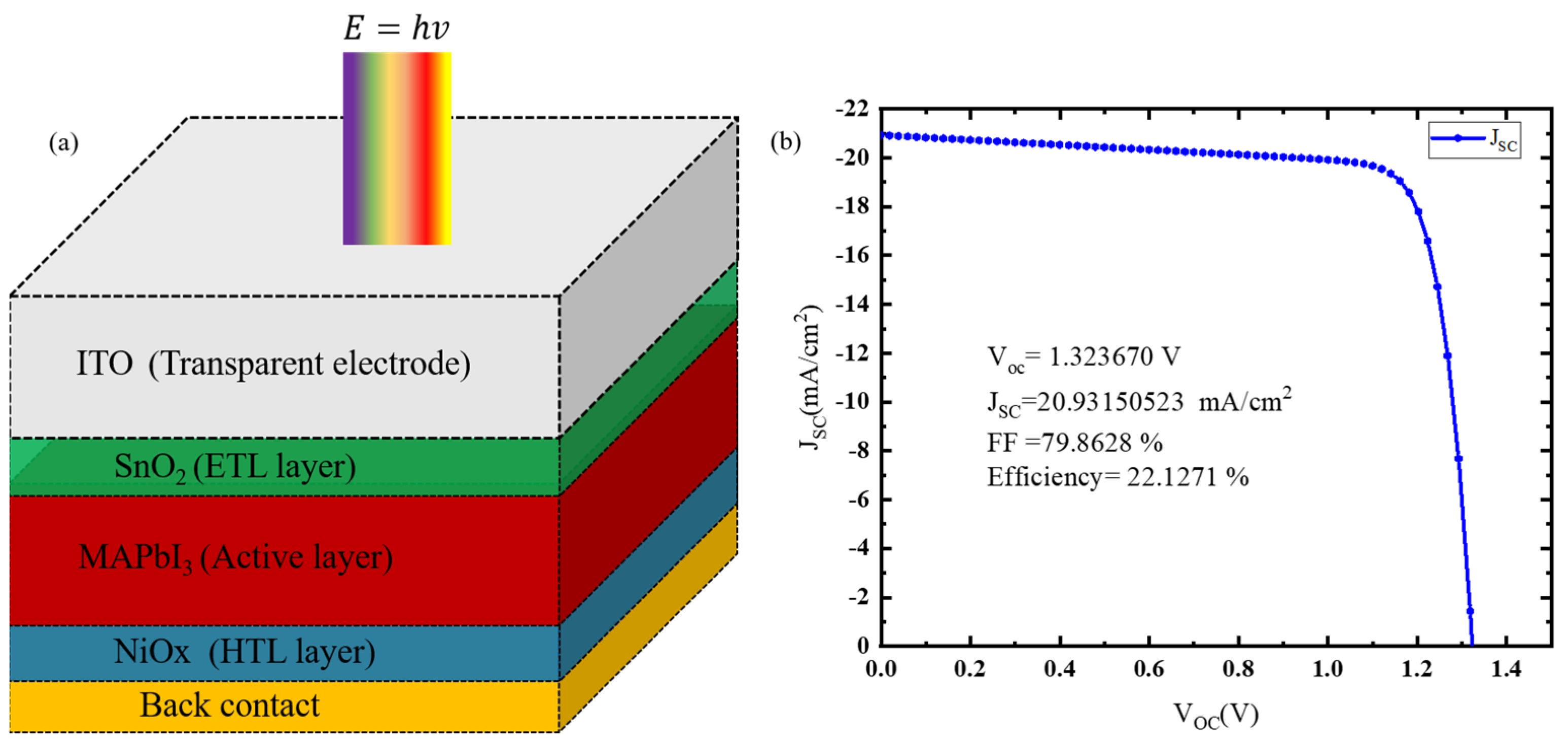
3. Proposed Device Model

The proposed Perovskite solar cell (PSC) layer configuration is shown in Figure 1a. The various electrical parameters of the material used in PSC simulation are shown in Table 1, while Table 2 display parameters taken for interference defects. The framework of the cell consists of ITO/SnO2/CH3NH3PbI3/NiOX/Back contact. The transparent electrode ITO serves two functions: anode collecting electron for an external load and passing light spectrum to the internal cell structure. SnO2 act as the ETL, which passes electrons easily while blocking the holes. The methylammonium lead iodide (CH3NH3PbI3) is a light-absorbing layer where electron-hole pairs are created under illumination. NiOX acts as the hole transport layer medium while blocking the electron. The overall device exhibits NIP configuration in which SnO2 is an n-type material, CH3NH3PbI3 as an intrinsic semiconductor, and NiOX is a p-type material. The selection of CTL materials in PSC design is crucial for the device’s performance, as efficient CTL layers provide higher conductivity and reduce recombination losses of carriers. The material used for the ETL typically has a LUMO (lowest un-occupied molecular orbital) energy lower than or equal to the LUMO energy of the active layer. The natural tendency of electrons to move from high to low energy levels facilitates electron transport while hindering the movement of holes. Similarly, HTL material should have a HOMO (highest occupied molecular orbital) energy equal to or higher than that of the active material. Holes always tend to move from low to higher energy levels. This mechanism ensures efficient hole transport while blocking electrons. The band alignment diagram of our proposed device is shown in Figure S1. All the simulations were performed at a standard test temperature of 300 K and a standard test illumination condition of 100 w/m2. The series and shunt resistance are considered 1 Ω.cm2 and 1.0 × 10³ Ω.cm2, respectively. The optimum thickness of the PSC was founded 300 nm/50 nm/400 nm/50 nm at which the cell recorded an efficiency of around 22.1%. In addition, the proper thickness of the CTL is required to avoid the short circuit effect in the cell structure due to sputtering damage.
Table 1. Material parameter used for simulation.
ParametersMaterials
ITO [34]NiOXCH3NH3PbI3SnO2
Thickness (nm)30050–200100–160050–200
Dielectric constant9.0010.7 [35]10.0 [35]8.00 [35]
Electron affinity (, χ (eV))4.002.1 [36]4.1 [37]3.93 [38]
Bandgap, Eg (eV)3.53.7 [39]1.6 [40,41]3.6 [38]
Effective conduction band density, Nc (cm−3)2.2 × 10182.8 × 1019 [42]2 × 10183.1 × 1018 [43]
Effective valence band density, Nv (cm−3)1.8 × 10191.8 × 1019 [42]1 × 10182.5 × 1019 [43]
Mobility of electron, μn (cm2/(V s))2012.0 [44]10015 [45]
Mobility of hole, μp (cm2/(V s))1025.0 [44]1000.1 [45]
Donor concentration ND (cm−3)1.0 × 10210.01 × 1091019
Acceptor concentration NA (cm−3)01 × 10151 × 1090.0
Defect density (1/cm3)1 × 10151 × 10141 × 10141 × 1014
Absorption coefficients (α)[46][47][47][47]
Table 2. Parameter used for interface defects [48].
ParametersETL/MAPbI3HTL/MAPbI3
Defect typeNeutralNeutral
Capture cross section of electrons (cm−2)1 × 10191 × 1019
Capture cross section of holes (cm−2)1 × 10−191 × 1019
Energetic distributionSingleSingle
Reference for defect energy level EtAbove the highest EV Above the highest EV
Reference energy (eV)0.60.6
Total density (1/cm2)1 × 1010–1 × 10201 × 1010–1 × 10²⁰

4. Result and Discussion

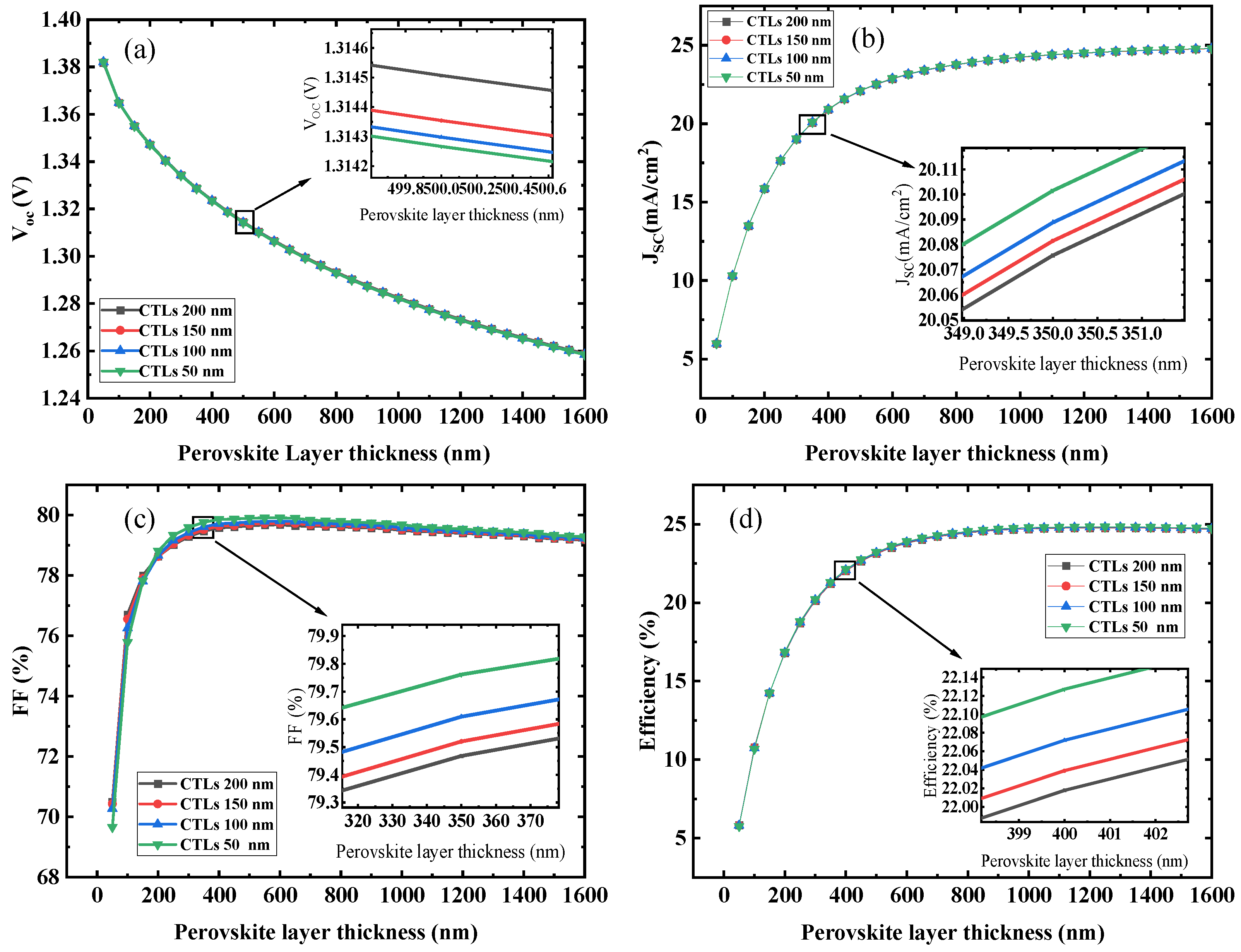
4.1. Effects of Layer Thickness

The thickness of the active or photon-absorbing layer (MAPbI3) has significant impacts on the PSC’s performance. A very thin absorbing layer harvesting a small portion of the photons create a smaller number of electron-hole pairs which directly reduce the efficiency of the solar cell. In contrast, a very thick absorber layer lowers the cell’s efficiency due to recombination losses [49,50]. Thus, it is essential to find the optimum thickness of MAPbI3. To determine the optimum thickness of the perovskite material layer, the thickness of the MAPbI3 is varied from 100 nm to 1600 nm, while in parallel, the thickness of the CTL layer is from 50 nm to 200 nm in four steps. The cell is simulated under standard test conditions (STCs) of 1000 w/m2 (A.M 1.5 G) and a standard test temperature (STT) of 300 K. The cell performance parameter such as VOC, η, FF, and JSC in response to layer thickness is shown in Figure 2. We observed VOC (Figure 2a) is directly affected by the increase in thickness due to the increase in parasitic resistance. The FF increases from 100 to 400 nm and then starts to decrease, which is also caused by the parasitic resistance. The increase in thickness ensures a larger area for photon absorption and hence a high number of electron-hole pairs resulting in high efficiency, above 400 nm the efficiency is slowly increased because of the low extraction rate of the carriers. The fundamental cause of the cell efficiency improvement with the thickness is due to the increase in optical density. However, when the diffusion length of the carrier is less than the active layer thickness, the carriers will recombine before crossing the CTL layer [23]. The other parameters, JSC and cell efficiency, increase logarithmically; at 400 nm MAPbI3 and 50 nm CTL thickness, the PSC efficiency reached 22.13%. It may be deduced that an increase in thickness beyond 400 nm can reduce the FF of the PSC. In addition to this, insubstantial improvements in efficiency come at the expense of material quantity, which is economically unacceptable. The optimal layer thicknesses for MAPbI3 and CTL are 400 nm and 50 nm, respectively. The J–V curve and the performance parameter of the cell at the optimum size is shown in Figure 1b.

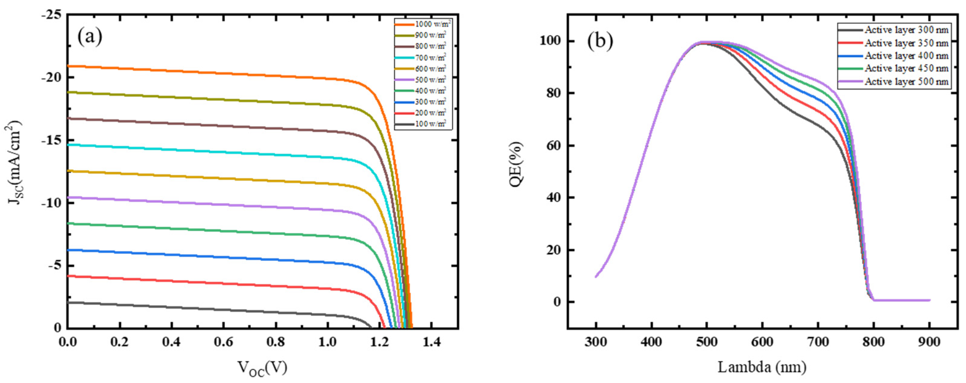
4.2. Effects of Light Intensity and Quantum Efficiency

The primary input source of energy that activates the solar cell is sunlight, and the intensity of the sunlight is not fixed and varies from 0 to 1 kw/m2 due to the continuous changing of the sun’s position. This illumination fluctuation greatly affects the solar cell’s performance [51]. To counter this problem, a solar tracking mechanism is introduced that allows solar module to track the sun’s daily passage from east to west or MPPT electrical device that manipulate the electrical parameter (voltage or current) to ensure high power is obtained from the solar cell [52]. The solar cell integrated with such an intriguing gadget offers continuous peak power throughout the daytime. AM1.5 G or 1 kw/m2 (equal to one sun) is a STC at which a commercial solar cell performance is measure before finalizing the product. Similarly, the value of 10 kw/m2 indicates that the cell is exposed to 10 suns. Although the number of 10 suns is technically impossible, it is indirectly employed for concentrated solar cells. The designed PSC is also tested under such circumstances. The light intensity is varied from 100 w/m2 to 1000 w/m2 at STC of 300 K. The J–V curve of the PSC’s various illumination intensities are shown in Figure 3a. We noticed that VOC and JSC are directly proportional to the intensity of light, which directly affects the output power and efficiency of the solar cell.
Similarly, quantum efficiency (QE) of the PV cell can be described by the ratio of the numbers of carrier captured by the cell to the incident number of photons of a given energy. It specifies how the device reacts to the various illumination wavelengths [53]. When photons of a given energy or wavelength are absorbed and the resultant minority’s carrier are accumulated, the QE is said to be at unity with that wavelength. QEs with different active layer thicknesses are shown in Figure 3b. QE as a function of lambda is investigated within the range of 300 nm to 900 nm. The QE rise from 300 nm to 800 nm, and the highest peak is observed between 450 nm to 550 nm, following the reduction in the QE and reaching zero. The square shape of the QE curve (ideal condition) is also affected by the active layer thickness of the solar cell, which is observed.

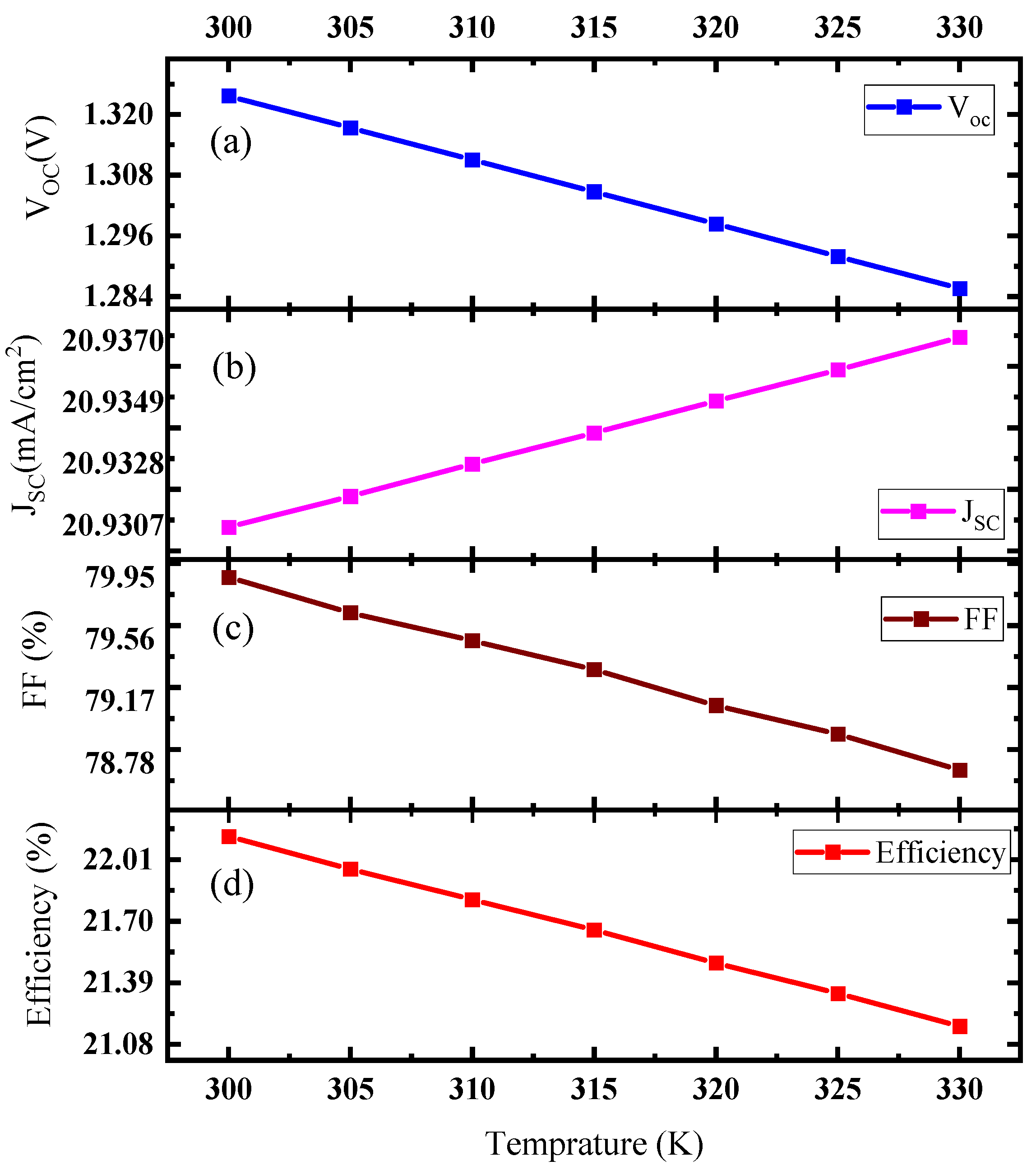
4.3. Effects of Temperature

The PSC performance is substantially affected by the operating temperature. Generally, STT 300 K is employed for simulation purposes. However, in natural environments, this number is not constant and changes over the year. High temperatures cause deformations in the cell structure, introducing interfacial defects between the composite layers of the cell [54]. These defects limit the interconnectivity of the PSC layer, resulting in a higher rate of recombination and a rise of parasitic resistance (RS) which decrease the PSC efficiency. Higher temperatures also affect electron-hole concentration, carrier mobility, and semiconductor bandgap [55]. The atomic vibration of the semiconductor is sensitive to the temperature. The increase in temperature speeds up atomic vibrations in the semiconductor, which causes an increase in inter-atomic separation. The linear temperature coefficient of a material is used to quantify this effect. As the interatomic space increases, the average electric potential perceived by the electron decreases, eliminating the bandgap size. The interatomic distance can also be changed by applying mechanical stress, resulting in a decrease or increase in the bandgap of the material. Vershni’s relation states that the bandgap of a material is temperature dependent and is given by
E g ( T ) = E g ( 0 ) α T 2 β + T
where T is the temperature, and E g ( 0 ) (bandgap at 0 K), β, and α are the material constants. In this simulation, we varied the temperature from 300 K to 330 K while keeping light intensity, parasitic resistance, and thickness of the layers constant. The influence of temperature on the solar cell’s performance, as illustrated in Figure 4, is of significance. At an operating temperature of 300 K, the VOC and FF measures at 1.323 V and 79.86%, respectively. However, as the temperature increases, there is a corresponding decrease in both VOC and FF, as depicted in Figure 4a,c, eventually resulting in values of 1.285 V and 78.65%, respectively. The JSC remains relatively constant around 20.93 mA/m2 (see Figure 4b). However, there is a slight increase from 0.0007 mA/m2 to 0.0070 mA/m2 due to the contribution of thermally generated carriers in addition to the light-generated carriers. The VOC and FF are directly influenced by the adverse effects of temperature, which consequently impacts the overall efficiency of the solar cell. Figure 4d illustrates a decline in efficiency from 22.12% to 21.17%, underscoring the temperature’s detrimental impact.

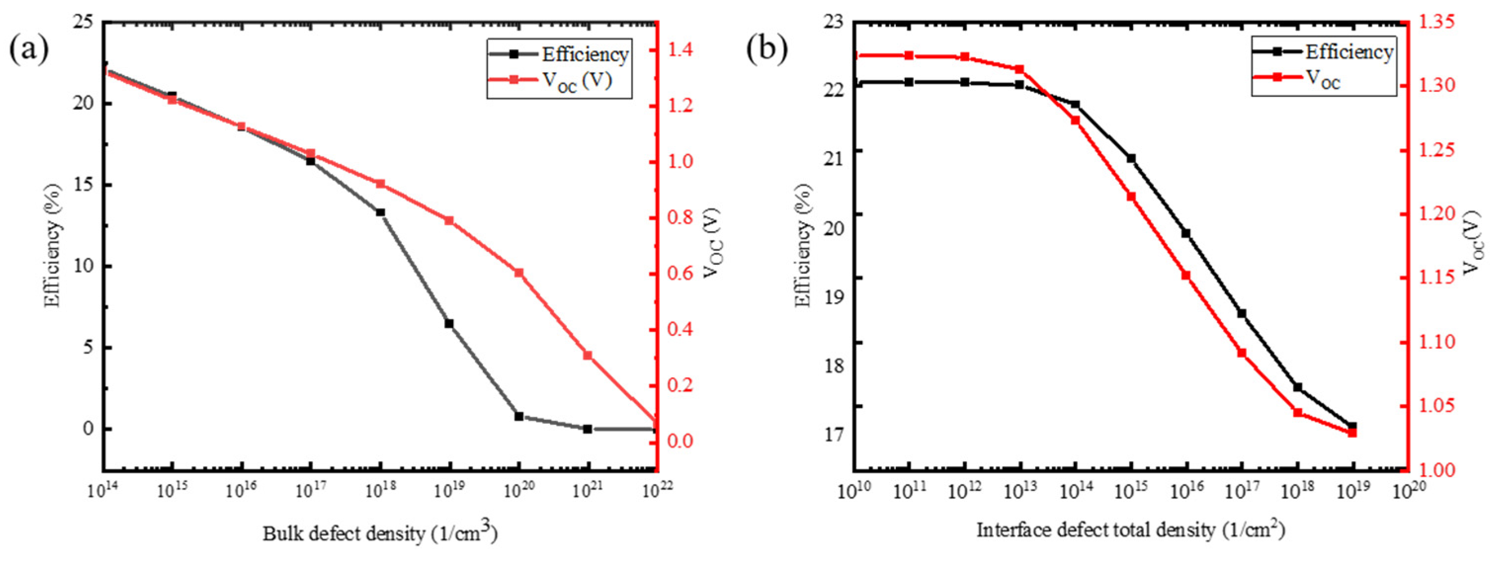
4.4. Effects of Bulk Defects and Interface Defects Density

SCAPS-1D uses the thermionic emission model (TEM) to explore heterojunction layers. Interface defects are analyzed in the same way as bulk defects, and a recombination in these states is assessed by an extension of the SRH theory known as the Pauwels–Vanhoutte theory [56]. These traps facilitate recombination losses, enhancing dark current and hence lowering efficiency. The carrier capture cross-section, energy level, and trap density are basic physical properties that determine how a certain trap impacts the non-radiative recombination rate. The carrier capture cross-section is mostly determined by the material’s dielectric constant, while trap density can be technically controlled by eliminating crystallographic defects such as surface and grain boundary imperfections throughout the fabrication process [57].
Elementary and neutral vacancy pair defects do not generate deep energy levels within the bandgap; only shallow traps are likely produced, which are not expected to act as potent recombination centers [57]. Furthermore, some contaminants in the PbI2 reactant, as well as Au residues absorbed in the active layer due to contact deposition, greatly affect the performance of the cell [58]. To prevent such defects that may result in deep traps, precise manufacturing techniques are required.
PSCs consist of different thin-film materials which are arranged in a sandwich-like structure. Poor deposition of thin-films leaves defects in the materials which greatly affect the performance of the cell [59]. Especially perovskite material exhibits distinct characteristics regarding longer diffusion lengths for electrons and holes (Ln and Lp) in a single crystal. However, this diffusion length significantly fluctuates in thin-film materials, depending upon the quality of the film [35]. In order to examine the impact of defects densities, we introduce defects ranging from 1 × 10¹⁴ to 1 × 1022 cm−3 in all layers of the PSC, including ETLs, HTLs, and perovskite layers.
Figure S2 shows variation in performance parameters such as JSC, VOC, FF, and efficiency follow the expected trend, with a visible reduction as the quality of the layer deteriorates (or defects density increase in thin-films). The VOC and JSC decrease from 1.313 V to 0.057 V and 20.77 to 0.06 mA/cm2, respectively. Similarly, FF and efficiency decrease from 79.55% to 24.96% and 22.03 to 0.72%, correspondingly, because of leakage current and parasitic resistance, the light-generated power is dissipated in the cell structure. The defects density of 1 × 10¹⁴ has a negligible impact, while above 1 × 10¹⁸, an abrupt decrease is noticed in the cell performance parameters. Defect concentrations in the range of 1 × 10¹⁴ to 1 × 10¹⁷ are considered acceptable for practical application. In our simulation, we chose a defect density of 1 × 10¹⁴, at which the efficiency and VOC of the cell is recorded 22.13% and 1.33 V, respectively. The impact of bulk defects on VOC efficiency are combinedly displayed in Figure 5a.
The junction quality plays a crucial role in the device’s performance. The presence of defects at the interface increases the recombination rate, resulting in inefficient performance [59,60]. Modeling recombination at the interface is a complex task, and the ideal approach is to introduce a thin defective layer between the junctions to study the effect of the defect at the interface. Here are two thin defective interface layers (DILs) at both sides of the perovskite material layer. The configuration of the cell becomes HTL/DIL/MAPbI3/DIL/ETL. The defect density is varied from 1010 cm−2 to 1020 cm−2. Figure 5b shows the parameter VOC and efficiency decrease with the increase in defect density at the interface. The DILs inserted between the HTL/MAPbI3 junction, ETL/MAPbI3 junction, or placed at both sides of the active layer give the same simulation results. However, the actual performance of the device will be disclosed upon the device fabrication and testing.

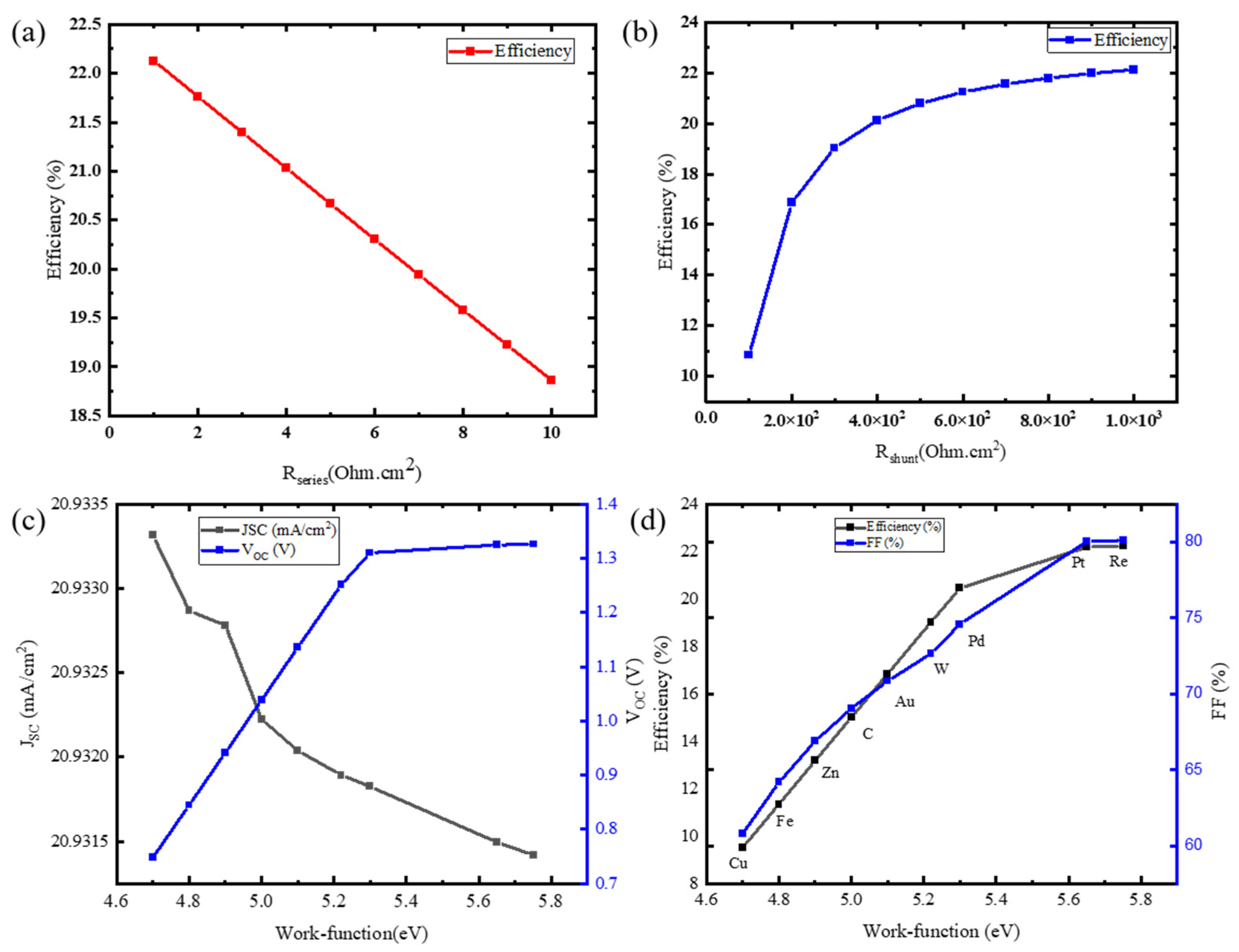
4.5. Effects of Parasitic Resistance and Work Function of Back Contact

Resistive effects within solar cells lead to a significant decrease in their efficiency. Some percentage of the light-generated power is dissipated in the cell structure due to these internal resistances. Series and shunt resistances (RS and RSH) are the two primary types of parasitic resistances (RP) [12,13]. The primary factors responsible for series resistance (RS) comprise the semiconductor material’s bulk resistance, interconnection of composite material layers between each other, metal/semiconductor ohmic contact, and the resistance of the electrode’s materials. The shunt resistance is due to the manufacturing defects in the solar cell structure which dissipate a significant amount of light power. Low RSH provides an alternate path to the carriers’ resulting loss of power and lowers the overall efficiency of the device [13]. The researcher tries to keep RS and RSH values at minimum and maximum values, respectively, for optimum design.
We investigated various RP values and their impacts on solar cell performance. We noticed that increasing RS from 1 to 10 Ω.cm2 has no effect on VOC and minimal influence on JSC. Other solar cell metrics such as efficiency and FF are constantly dropping with the increase in series resistance (see Figure S3). Similarly, the RSH is varied from 0.1 × 10³ to 1.0 × 10³ Ω.cm2 (see Figure S4), which shows that VOC, FF, JSC, and efficiency are improving. The corresponding graph pattern of various parameters shows a significant rise with the increase in shunt resistance. A sharp rise up to 0.4 × 10³ is visible, followed by a gradual gain with each further increment in RSH. In our simulation, the values for RS and RSH are considerd 1 Ω.cm2 and 1.0 × 10³ Ω.cm2, respectively, at which point the efficiency reached 22.13% (Figure 6a,b).
The work function and material of the back electrode have a considerable impact on built-in voltage (Vbi) of a PV cell, resulting in an increase in RS of the cell and a decrease in efficiency [61]. A number of materials with different work functions are investigated for the backend electrode to see how they affect the solar cell characteristics, while keeping the front transparent electrode constant. Various materials with different work functions were investigated, including Cu, Fe, Zn, C, Au, W, Pd, Pt, and Re [61,62,63], to determine how the work function influences solar cell performance. The impact of various materials and their associated work functions on JSC and VOC is depicted in Figure 6c. This shows that the work function has little effect on JSC but a substantial impact on VOC. Similarly, as the work function increases from 4.7 eV to 5.65 eV, efficiency and FF (Figure 6d) improve significantly. This enhancement is due to a reduction in the Schottky barrier height between the anode and the HTL, which allows holes to travel more easily from the HTL to the backside of the electrode. Although gold has a reasonable work function for simulation, silver and aluminum are more cost-effective options for the experimentation and commercialization of the solar cell.

5. Conclusions

In this research, MAPbI3-based PSCs were arranged in NIP configurations of ITO/SnO2/CH3NH3PbI3/NiOX/Back contact and simulated under standard test conditions of 300 K and A.M 1.5 G. The primary goal is to investigate PSCs with inorganic CTL layers that are easily deposited though the ALD method in order to enhance the efficiency and stability of the cell. We optimized the device using a comprehensive layer-by-layer methodology, including a MAPbI3 and CTL layer. The optimum thickness of the active and CTL layer was found to be 400 nm and 50 nm, respectively, while taking the bulk defect density of 1 × 1014 cm−3 in all layers as a constant. In this arrangement, the PSC obtained showed an efficiency of 22.13%, VOC of 1.32, JSC of 20.93 mA/m2, and FF of 79.89%. We also introduced interface defects (1010 cm−2 to1020 cm−2) between the CTL and perovskite layer; the increase in interface defects can cause poor efficiency of the device which can be eliminated with ALD deposition. Similarly, the influence of parasitic resistance indicates the significance of small RS and high values of RSH. The design cell’s RS and RSH values are taken to be 1.0 Ω.cm2 and 1.0 × 10³ Ω.cm2, respectively. The work function of ITO is set constant of 4.13 eV, while the different materials have different work functions being tested for back contact at 5.65 eV, and the PSC shows the highest efficiency of 22.13%. In addition, cell parameters are also examined under various practical operating conditions, such as the impact of temperature and light intensity. The design cell’s possible parameter aspects are numerically tested and analyzed; however, it is necessary to disclose the stability of the cell structure’s with ALD fabrication.

Supplementary Materials

The following supporting information can be downloaded at: https://www.mdpi.com/article/10.3390/en16217438/s1, Figure S1: PSC band alignment diagram; Figure S2: Effect of bulk defects in the cell structure; Figure S3: Effect of series resistance; Figure S4: Effect of shunt resistance.

Author Contributions

Conceptualization, S.M. and Y.X.; methodology, S.M., F.Q. and Y.X.; software, S.M.; validation, S.M., F.Q. and M.H.; formal analysis, S.M.; investigation, Y.X. and F.Q.; writing—original draft preparation, S.M., F.Q. and Y.X.; writing—review and editing, S.M. and F.Q.; supervision, Y.X.; project administration, Y.X. and F.Q.; funding acquisition, M.H. All authors have read and agreed to the published version of the manuscript.

Funding

This work was supported in part by Key Research and Development Program of the Chinese Ministry of Science and Technology under Contract 2018YFA0704800, Research and Development Project of Scientific Instruments and Equipment of the Chinese Academy of Sciences under Contract ZDKYYQ20220001 and Research and Development Projects of the Northern Integrated Circuit Technology Innovation Center under contract QYJS-2022-1802-B.

Informed Consent Statement

Not applicable.

Data Availability Statement

Not applicable.

Conflicts of Interest

The authors declare no conflict of interest.

References

  1. Gagliardi, A.; Abate, A. Mesoporous Electron-Selective Contacts Enhance the Tolerance to Interfacial Ion Accumulation in Perovskite Solar Cells. Am. Chem. Soc. 2018, 3, 163–169. [Google Scholar] [CrossRef]
  2. Seo, S.; Jeong, S.; Park, H.; Shin, H.; Park, N.G. Atomic layer deposition for efficient and stable perovskite solar cells. Chem. Commun. 2019, 55, 2403–2416. [Google Scholar] [CrossRef] [PubMed]
  3. Ma, T.; Song, Q.; Tadaki, D.; Niwano, M.; Hirano-Iwata, A. Unveil the Full Potential of Integrated-Back-Contact Perovskite Solar Cells Using Numerical Simulation. ACS Appl. Energy Mater. 2018, 1, 970–975. [Google Scholar] [CrossRef]
  4. Zhao, P.; Lin, Z.; Wang, J.; Yue, M.; Hao, Y. Numerical simulation of planar heterojunction perovskite solar cells based on SnO2 electron transport layer. ACS Appl. Energy Mater. 2019, 2, 4504–4512. [Google Scholar] [CrossRef]
  5. Bisquert, J.; Qi, Y.; Ma, T.; Yan, Y. Advances and Obstacles on Perovskite Solar Cell Research from Material Properties to Photovoltaic Function. ACS Energy Lett. 2017, 2, 520–523. [Google Scholar] [CrossRef]
  6. Cameron, J.; Skabara, P.J. The damaging effects of the acidity in PEDOT:PSS on semiconductor device performance and solutions based on non-acidic alternatives. Mater. Horiz. 2020, 7, 1759–1772. [Google Scholar] [CrossRef]
  7. Kim, H.S.; Seo, J.Y.; Park, N.G. ChemInform Abstract: Material and Device Stability in Perovskite Solar Cells. ChemInform 2016, 9, 2528–2540. [Google Scholar] [CrossRef]
  8. Lee, S.W.; Kim, S.; Bae, S.; Cho, K.; Chung, T.; Mundt, L.E.; Lee, S.; Park, S.; Park, H.; Schubert, M.C. UV Degradation and Recovery of Perovskite Solar Cells. Sci. Rep. 2016, 6, 38150. [Google Scholar] [CrossRef]
  9. Hossain, M.A.; Khoo, K.T.; Cui, X.; Poduval, G.K.; Zhang, T.; Li, X.; Li, W.M.; Hoex, B. Atomic layer deposition enabling higher efficiency solar cells: A review. Nano Mater. Sci. 2020, 2, 204–226. [Google Scholar] [CrossRef]
  10. Lee, Y.; Jeon, N.; Kim, B.; Shim, H.; Yang, T.Y.; Seok, S.I.; Seo, J.; Im, S.G. A Low-Temperature Thin-Film Encapsulation for Enhanced Stability of a Highly Efficient Perovskite Solar Cell. Adv. Energy Mater. 2018, 8, 1701928. [Google Scholar] [CrossRef]
  11. Lübke, D.; Hartnagel, P.; Hülsbeck, M.; Kirchartz, T. Understanding the Thickness and Light-Intensity Dependent Performance of Green-Solvent Processed Organic Solar Cells. ACS Mater. Au 2023, 3, 215–230. [Google Scholar] [CrossRef]
  12. Saikrishna, G.; Parida, S.; Behera, R. Effect of parasitic resistance in solar photovoltaic panel under partial shaded condition. In Proceedings of the 2015 International Conference on Energy Systems and Applications, Pune, India, 30 October–1 November 2015; IEEE: Piscataway, NJ, USA, 2015; pp. 396–401. [Google Scholar]
  13. Van Dyk, E.; Meyer, E.L. Analysis of the effect of parasitic resistances on the performance of photovoltaic modules. Renew. Energy 2004, 29, 333–344. [Google Scholar] [CrossRef]
  14. Wen, L.; Zhou, M.; Wang, C.; Mi, Y.; Lei, Y. Energy Storage: Nanoengineering Energy Conversion and Storage Devices via Atomic Layer Deposition. Adv. Energy Mater. 2016, 6, 1600468. [Google Scholar] [CrossRef]
  15. Hossain, M.K.; Ishraque Toki, G.; Samajdar, D.; Rubel, M.; Mushtaq, M.; Islam, M.R.; Rahman, M.F.; Bhattarai, S.; Bencherif, H.; Mohammed, M.K. Photovoltaic performance investigation of Cs3Bi2I9-based perovskite solar cells with various charge transport channels using DFT and SCAPS-1D frameworks. Energy Fuels 2023, 37, 7380–7400. [Google Scholar] [CrossRef]
  16. Saha, N.; Brunetti, G.; Armenise, M.N.; Carlo, A.D.; Ciminelli, C. Modeling Highly Efficient Homojunction Perovskite Solar Cells With Graphene-TiO2 Nanocomposite as the Electron Transport Layer. IEEE J. Photovolt. 2023, 13, 705–710. [Google Scholar] [CrossRef]
  17. Mushtaq, S.; Tahir, S.; Ashfaq, A.; Sebastian Bonilla, R.; Haneef, M.; Saeed, R.; Ahmad, W.; Amin, N. Performance optimization of lead-free MASnBr3 based perovskite solar cells by SCAPS-1D device simulation. Sol. Energy 2023, 249, 401–413. [Google Scholar] [CrossRef]
  18. Hussain, C.; Hassan, Y.; Abed, F. Optimization of Organic-Inorganic Perovskite Solar Cell Layers. In Research Square. 2022. Available online: https://www.researchsquare.com/article/rs-2084341/v1 (accessed on 23 September 2023).
  19. Sunny, A.; Rahman, S.; Khatun, M.M.; Ahmed, S.R.A. Numerical study of high performance HTL-free CH3NH3SnI3-based perovskite solar cell by SCAPS-1D. AIP Adv. 2021, 11, 065102. [Google Scholar] [CrossRef]
  20. Ibrahim, H.K.; Sabaawi, A.M.A.; Algwari, Q.T. Study of defects in CH3NH3PbI3-based perovskite solar cells. IOP Conf. Ser. Mater. Sci. Eng. 2021, 1152, 012032. [Google Scholar] [CrossRef]
  21. Samiul Islam, M.; Sobayel, K.; Al-Kahtani, A.; Islam, M.A.; Muhammad, G.; Amin, N.; Shahiduzzaman, M.; Akhtaruzzaman, M. Defect Study and Modelling of SnX3-Based Perovskite Solar Cells with SCAPS-1D. Nanomaterials 2021, 11, 1218. [Google Scholar] [CrossRef]
  22. Basyoni, M.S.S.; Salah, M.M.; Mousa, M.; Shaker, A.; Zekry, A.; Abouelatta, M.A.; Alshammari, M.T.; Al-Dhlan, K.A.; Gontrand, C. On the Investigation of Interface Defects of Solar Cells: Lead-Based vs Lead-Free Perovskite. IEEE Access 2021, 9, 130221–130232. [Google Scholar] [CrossRef]
  23. Mehmood, S.; Kaleem, M.; Nazir, S.; Israr, A.; Mirza, H.T. Numerical Analysis of Stable and Low Cost Perovskite Solar Cell with an Enhanced Inorganic Electron and Hole Transport Layers. J. Nanoelectron. Optoelectron. 2020, 15, 725–733. [Google Scholar] [CrossRef]
  24. Islam, M.B.; Yanagida, M.; Shirai, Y.; Nabetani, Y.; Miyano, K. NiOx Hole Transport Layerfor Perovskite Solar Cells with Improved Stability and Reproducibility. ACS Omega 2017, 2, 2291–2299. [Google Scholar] [CrossRef] [PubMed]
  25. Hsu, C.-C.; Yu, S.-M.; Lee, K.-M.; Lin, C.-J.; Liou, B.-Y.; Chen, F.-R. Oxidized nickel to prepare an inorganic hole transport layer for high-efficiency and stability of CH3NH3PbI3 perovskite solar Cells. Energies 2022, 15, 919. [Google Scholar] [CrossRef]
  26. Li, Y.; Zhu, J.; Huang, Y.; Liu, F.; Lv, M.; Chen, S.; Hu, L.; Tang, J.; Yao, J.; Dai, S. Mesoporous SnO2 nanoparticle films as electron-transporting material in perovskite solar cells. RSC Adv. 2015, 5, 28424–28429. [Google Scholar] [CrossRef]
  27. Ke, W.; Fang, G.; Liu, Q.; Xiong, L.; Qin, P.; Tao, H.; Wang, J.; Lei, H.; Li, B.; Wan, J. Low-temperature solution-processed tin oxide as an alternative electron transporting layer for efficient perovskite solar cells. J. Am. Chem. Soc. 2015, 137, 6730–6733. [Google Scholar] [CrossRef] [PubMed]
  28. Kavan, L.; Steier, L.; Grätzel, M. Ultrathin buffer layers of SnO2 by atomic layer deposition: Perfect blocking function and thermal stability. J. Phys. Chem. C 2017, 121, 342–350. [Google Scholar] [CrossRef]
  29. Ke, W.; Zhao, D.; Cimaroli, A.J.; Grice, C.R.; Qin, P.; Liu, Q.; Xiong, L.; Yan, Y.; Fang, G. Effects of annealing temperature of tin oxide electron selective layers on the performance of perovskite solar cells. J. Mater. Chem. A 2015, 3, 24163–24168. [Google Scholar] [CrossRef]
  30. Qin, X.; Zhao, Z.; Wang, Y.; Wu, J.; Jiang, Q.; You, J. Recent progress in stability of perovskite solar cells. J. Semicond. 2017, 38, 011002. [Google Scholar] [CrossRef]
  31. Lin, S.; Yang, B.; Qiu, X.; Yan, J.; Shi, J.; Yuan, Y.; Tan, W.; Liu, X.; Huang, H.; Gao, Y. Efficient and stable planar hole-transport-material-free perovskite solar cells using low temperature processed SnO2 as electron transport material. Org. Electron. 2018, 53, 235–241. [Google Scholar] [CrossRef]
  32. Wu, P.; Wang, S.; Li, X.; Zhang, F. Advances in SnO2-based perovskite solar cells: From preparation to photovoltaic applications. J. Mater. Chem. A 2021, 9, 19554. [Google Scholar] [CrossRef]
  33. Burgelman, M.; Decock, K.; Khelifi, S.; Abass, A. Advanced electrical simulation of thin film solar cells. Thin Solid Film. 2013, 535, 296–301. [Google Scholar] [CrossRef]
  34. Abdelaziz, S.; Zekry, A.; Shaker, A.; Abouelatta, M. Investigating the performance of formamidinium tin-based perovskite solar cell by SCAPS device simulation. Opt. Mater. 2020, 101, 109738. [Google Scholar] [CrossRef]
  35. Rahman, M.S.; Miah, S.; Marma, M.S.W.; Sabrina, T. Simulation based investigation of inverted planar perovskite solar cell with all metal oxide inorganic transport layers. In Proceedings of the 2019 International Conference on Electrical, Computer and Communication Engineering (ECCE), Chittagong, Bangladesh, 7–9 February 2019; IEEE: Piscataway, NJ, USA, 2019; pp. 1–6. [Google Scholar]
  36. Ratcliff, E.L.; Meyer, J.; Steirer, K.X.; Armstrong, N.R.; Olson, D.; Kahn, A. Energy level alignment in PCDTBT: PC70BM solar cells: Solution processed NiOx for improved hole collection and efficiency. Org. Electron. 2012, 13, 744–749. [Google Scholar] [CrossRef]
  37. Goje, A.; Ludin, N.; Teridi, M.M.; Syafiq, U.; Ibrahim, M.; Nawab, F.; Syakirin, A. Design and Simulation of Lead-Free Flexible Perovskite Solar cell Using SCAPS-1D. In Proceedings of the International Conference on Sustainable, Renewable & Energy Efficiency, Bangi, Malaysia, 7–8 November 2022; IOP Conference Series: Materials Science and Engineering. IOP Publishing: Bristol, England, 2023; p. 012004. [Google Scholar]
  38. Baena, J.P.C.; Steier, L.; Tress, W.; Saliba, M.; Neutzner, S.; Matsui, T.; Giordano, F.; Jacobsson, T.J.; Kandada, A.R.S.; Zakeeruddin, S.M. Highly efficient planar perovskite solar cells through band alignment engineering. Energy Environ. Sci. 2015, 8, 2928–2934. [Google Scholar] [CrossRef]
  39. Tian, H.; Fan, H.; Dong, G.; Ma, L.; Ma, J. NiO/ZnOp–n heterostructures and their gas sensing properties for reduced operating temperature. RSC Adv. 2016, 6, 109091–109098. [Google Scholar] [CrossRef]
  40. Eom, K.; Kwon, U.; Kalanur, S.S.; Park, H.J.; Seo, H. Depth-resolved band alignments of perovskite solar cells with significant interfacial effects. J. Mater. Chem. A 2017, 5, 2563–2571. [Google Scholar] [CrossRef]
  41. Castro, E.; Cerón, M.R.; Garcia, A.H.; Kim, Q.; Etcheverry-Berríos, A.; Morel, M.J.; Díaz-Torres, R.; Qian, W.; Martinez, Z.; Mendez, L. A new family of fullerene derivatives: Fullerene-curcumin conjugates for biological and photovoltaic applications. RSC Adv. 2018, 8, 41692–41698. [Google Scholar] [CrossRef] [PubMed]
  42. Rödl, C.; Schleife, A. Photoemission spectra and effective masses of n-and p-type oxide semiconductors from first principles: ZnO, CdO, SnO2, MnO, and NiO. Phys. Status Solidi A 2014, 211, 74–81. [Google Scholar] [CrossRef]
  43. Olson, D.C.; Ginley, D.S. Nanostructured TCOs (ZnO, TiO2, and Beyond). In Handbook of Transparent Conductors; Springer: Berlin/Heidelberg, Germany, 2011; pp. 425–457. [Google Scholar]
  44. Shan, F.; Liu, A.; Zhu, H.; Kong, W.; Liu, J.; Shin, B.; Fortunato, E.; Martins, R.; Liu, G. High-mobility p-type NiOx thin-film transistors processed at low temperatures with Al2O3 high-k dielectric. J. Mater. Chem. C 2016, 4, 9438–9444. [Google Scholar] [CrossRef]
  45. Farahani, S.V.; Veal, T.D.; Mudd, J.J.; Scanlon, D.O.; Watson, G.; Bierwagen, O.; White, M.; Speck, J.S.; McConville, C.F. Valence-band density of states and surface electron accumulation in epitaxial SnO2 films. Phys. Rev. B 2014, 90, 155413. [Google Scholar] [CrossRef]
  46. Holman, Z.C.; Filipič, M.; Descoeudres, A.; De Wolf, S.; Smole, F.; Topič, M.; Ballif, C. Infrared light management in high-efficiency silicon heterojunction and rear-passivated solar cells. J. Appl. Phys. 2013, 113, 013107. [Google Scholar] [CrossRef]
  47. Manzoor, S.; Häusele, J.; Bush, K.A.; Palmstrom, A.F.; Carpenter, J.; Zhengshan, J.Y.; Bent, S.F.; Mcgehee, M.D.; Holman, Z.C. Optical modeling of wide-bandgap perovskite and perovskite/silicon tandem solar cells using complex refractive indices for arbitrary-bandgap perovskite absorbers. Opt. Express 2018, 26, 27441–27460. [Google Scholar] [CrossRef] [PubMed]
  48. Jimoh, O.M.; Florence, I.N.; Akinbolati, A.; Nnachi, C.; Ajani, C.; Gyuk, P.M.; Magaji, S.; Danladi, E. Investigating the Performance of Perovskite Solar Cells Using Nickel Oxide and Copper Iodide as P-type Inorganic layers by SCAPS-1D Simulation. Phys. Access 2022, 37–50. [Google Scholar] [CrossRef]
  49. Sajid, S.; Elseman, A.M.; Ji, J.; Dou, S.; Wei, D.; Huang, H.; Cui, P.; Xi, W.; Chu, L.; Li, Y. Computational study of ternary devices: Stable, low-cost, and efficient planar perovskite solar cells. Nano-Micro Lett. 2018, 10, 51. [Google Scholar] [CrossRef]
  50. Yasodharan, R.; Senthilkumar, A.; Ajayan, J.; Mohankumar, P. Effects of layer thickness on Power Conversion Efficiency in Perovskite solar cell: A numerical simulation approach. In Proceedings of the 2019 5th International Conference on Advanced Computing & Communication Systems (ICACCS), Coimbatore, India, 15–16 March 2019; IEEE: Piscataway, NJ, USA, 2019; pp. 1132–1135. [Google Scholar]
  51. Stockhausen, V.; Andrade, L.; Ivanou, D.; Stannowski, B.; Mendes, A. Incident angle and light intensity variation: A comparative impact study on perovskite, Dye-sensitized and silicon heterojunction solar cells towards building-integrated applications. Sol. Energy Mater. Sol. Cells 2019, 191, 451–458. [Google Scholar] [CrossRef]
  52. Katche, M.L.; Makokha, A.B.; Zachary, S.O.; Adaramola, M.S. A comprehensive review of maximum power point tracking (mppt) techniques used in solar pv systems. Energies 2023, 16, 2206. [Google Scholar] [CrossRef]
  53. Gholami-Milani, A.; Ahmadi-Kandjani, S.; Olyaeefar, B.; Kermani, M.H. Performance analyses of highly efficient inverted all-perovskite bilayer solar cell. Sci. Rep. 2023, 13, 8274. [Google Scholar] [CrossRef]
  54. Schwenzer, J.A.; Rakocevic, L.; Gehlhaar, R.; Abzieher, T.; Gharibzadeh, S.; Moghadamzadeh, S.; Quintilla, A.; Richards, B.S.; Lemmer, U.; Paetzold, U.W. Temperature variation-induced performance decline of perovskite solar cells. ACS Appl. Mater. Interfaces 2018, 10, 16390–16399. [Google Scholar] [CrossRef]
  55. Varshni, Y.P. Temperature dependence of the energy gap in semiconductors. Physica 1967, 34, 149–154. [Google Scholar] [CrossRef]
  56. Pauwels, H.J.; Vanhoutte, G. The influence of interface state and energy barriers on the efficiency of heterojunction solar cells. J. Phys. D Appl. Phys. 1978, 11, 649–667. [Google Scholar] [CrossRef]
  57. Haider, S.Z.; Anwar, H.; Wang, M. A comprehensive device modelling of perovskite solar cell with inorganic copper iodide as hole transport material. Semicond. Sci. Technol. 2018, 33, 035001. [Google Scholar] [CrossRef]
  58. Tress, W. Perovskite Solar Cells on the Way to Their Radiative Efficiency Limit—Insights Into a Success Story of High Open-Circuit Voltage and Low Recombination. Adv. Energy Mater. 2017, 7, 1602358. [Google Scholar] [CrossRef]
  59. Jamal, M.; Shahahmadi, S.; Wadi, M.A.A.; Chelvanathan, P.; Asim, N.; Misran, H.; Hossain, M.; Amin, N.; Sopian, K.; Akhtaruzzaman, M. Effect of defect density and energy level mismatch on the performance of perovskite solar cells by numerical simulation. Optik 2019, 182, 1204–1210. [Google Scholar] [CrossRef]
  60. Chouhan, A.S.; Jasti, N.P.; Avasthi, S. Effect of interface defect density on performance of perovskite solar cell: Correlation of simulation and experiment. Mater. Lett. 2018, 221, 150–153. [Google Scholar] [CrossRef]
  61. Jan, S.T.; Noman, M. Influence of layer thickness, defect density, doping concentration, interface defects, work function, working temperature and reflecting coating on lead-free perovskite solar cell. Sol. Energy 2022, 237, 29–43. [Google Scholar]
  62. Lakhdar, N.; Hima, A. Electron transport material effect on performance of perovskite solar cells based on CH3NH3GeI3. Opt. Mater. 2020, 99, 109517. [Google Scholar] [CrossRef]
  63. Ngoupo, A.T.; Ouédraogo, S.; Zougmoré, F.; Ndjaka, J. Numerical analysis of ultrathin Sb2Se3-based solar cells by SCAPS-1D numerical simulator device. Chin. J. Phys. 2021, 70, 1–13. [Google Scholar] [CrossRef]
Figure 1. (a) Proposed PSC layer configuration; (b) optimum J-V curve.
Energies 16 07438 g001
Figure 2. Optimization of MAPbI3 and CTLs layer thickness on solar cell parameters:(a) Open-circuit voltage (b) Short-circuit current density (c) Fill factor (d) Efficiency.
Energies 16 07438 g002
Figure 3. (a) Impact of light intensity on VOC and JSC; (b) quantum efficiency in response to wave-length.
Energies 16 07438 g003
Figure 4. Effect of temperature on PSC performance parameter:(a) Open-circuit voltage (b) Short-circuit current density (c) Fill factor (d) Efficiency.
Energies 16 07438 g004
Figure 5. Effects of defects density: (a) bulk defects density; (b) interface defects density.
Energies 16 07438 g005
Figure 6. (a) Influence of shunt resistance on efficiency; (b) efficiency of PSC increases with the increase in shunt resistance; (c) impact of work function on VOC and JSC; (d) impact of work function on FF and efficiency.
Energies 16 07438 g006
Disclaimer/Publisher’s Note: The statements, opinions and data contained in all publications are solely those of the individual author(s) and contributor(s) and not of MDPI and/or the editor(s). MDPI and/or the editor(s) disclaim responsibility for any injury to people or property resulting from any ideas, methods, instructions or products referred to in the content.

