Article

Differential Power Processing Converter with an Integrated Transformer and Secondary Switch for Power Generation Optimization of Multiple Photovoltaic Submodules

1
Department of Electrical Engineering, Incheon National University, Incheon 22012, Korea
2
Advanced Electrification Engineering Design Team, Hyundai Motor Company, Hwaseong 18280, Korea
*
Author to whom correspondence should be addressed.
Energies 2022, 15(3), 1210; https://doi.org/10.3390/en15031210
Submission received: 13 January 2022 / Revised: 30 January 2022 / Accepted: 3 February 2022 / Published: 7 February 2022
(This article belongs to the Collection "Electric Vehicles" Section: Review Papers)

Abstract

:
In recent years, to increase the fuel efficiency of environment-friendly vehicles, a large volume of research is ongoing regarding applying photovoltaic (PV) systems. However, in PV systems, a power imbalance between submodules is common due to shading or pollution, and this degrades the power generation efficiency of the system. To solve this problem, various differential power processing (DPP) converters have been developed. In order to adopt the DPP converter to environment-friendly vehicles, the DPP converter must have a small volume, high efficiency, and high price competitiveness. In this regard, we propose a DPP converter with a single multi-winding transformer by integrating multiple transformers and secondary sides of the conventional flyback DPP converter. Since the proposed DPP converter can be applied to battery balancing circuits as well as photovoltaic systems, the proposed circuit is a valuable converter. In the PV system, the maximum output power of each submodule is 60 W, and the total PV system is 240 W by connecting four submodules in series. To verify the validity of the proposed DPP converter, a prototype with 8 V input and 60 W/30 V output specification was built and tested, and the effectiveness of the proposed converter is supported by the experimental results.

1. Introduction

Owing to their ability to improve fuel-efficiency, photovoltaic (PV) systems have been extensively applied in a wide range of environment-friendly vehicles, from Hybrid Electric Vehicles (HEVs) and Electric Vehicles (EVs) to mass-produced ones [1]. In addition, large-capacity PV systems have also been installed on the roofs of electric buses and trucks. In these PV systems, the PV submodules are connected in both series and parallel to generate high voltage and sufficient power. However, due to partial shading and contamination of the PV submodules, variations in power and current occur in the submodules, which, in turn, results in limited output power and small current in submodules. The power generation efficiency, thus, becomes considerably degraded [2]. In the PV system, excessive power dissipation, known as hot spotting, occurs due to cell reverse biasing [3].
To overcome the drawbacks of the PV system, various converters, such as DC optimizer [4,5] and cascaded converters [6,7], have been introduced, which can improve the power generation efficiency and solve the hot spot problem of the PV system. However, since these converters have to handle the rated power of each submodule or total system, other problems, such as bulky volume of the converter and the loss of the entire system creep in [8]. For small volume and low loss of converters, a differential power processing (DPP) converter that can only handle power differences between the submodules was proposed [9]. These DPP converters have a variety of architectures, such as PV–Bus [10,11,12,13], PV–PV [14,15,16], and PV–isolated port (IP) [17,18]. For the PV–PV converter topology, the bidirectional buck-boost converter is commonly used, and for the PV–IP and PV–Bus converter topology, the bidirectional flyback converter is widely applied as the DPP converter.
The DPP converters with the PV–IP architecture are installed between the PV submodules and the IP to achieve maximum power out of the total system via distributing the excessive power to the low-power submodules and thereby mitigating any current differences between submodules [19]. Figure 1a shows the PV–IP architecture, and Figure 1b shows the circuit diagram when the bidirectional flyback DPP converters are utilized with the PV–IP architecture. Assuming that the number of submodules in the conventional DPP converters are N, then N transformers, N primary and secondary side switches, and 2 N driving circuits are required, and due to these several components, the volume of magnetics and switches also increases.
Moreover, assuming that there is an imbalance in the power and energy of submodules in the PV system, since a transformer of the conventional flyback DPP converter stores and transmits imbalanced energy, the magnetizing current of the transformer has an offset that causes a large volume. Thus, conventional DPP converters are difficult to use in applications that require small volume and high price competitiveness, such as environmentally friendly vehicles. To address this issue, the current research aimed to introduce a new DPP converter with a single integrated transformer with PV–IP architecture.
The proposed DPP converter achieved high power density by integrating the transformer and secondary side switches. Thus, the proposed converter can improve the price competitiveness by reducing components. Moreover, it also improved efficiency by reducing conduction loss and switching loss. In addition, the compensation of power generation imbalance among PV submodules is possible since the imbalanced power is transferred and delivered through the transformer when all primary switches are turned on at the same time. Moreover, the proposed DPP converter can be used as the battery cell balancing circuit because it can equalize the power difference [20].
This paper is organized as follows. In Section 2, the characteristics and operation principle of the proposed DPP converter are explained, and the design method of the proposed DPP converter is presented via Section 3. The effectiveness of the proposed converter is supported by the experimental results with a 8 V input, 60 W and 30 V output prototype.

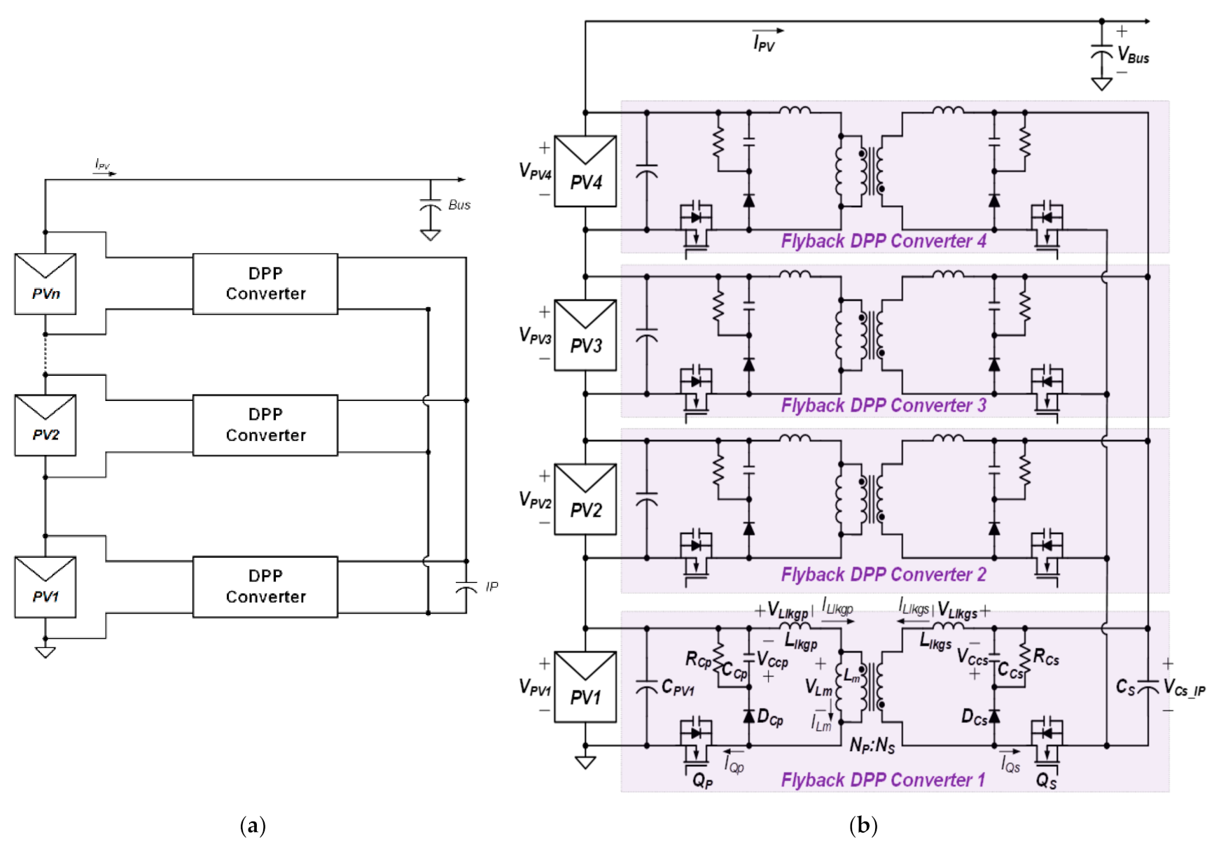
2. The Proposed DPP Converter

2.1. Characeristics of the Proposed DPP Converter

As shown in Figure 1, a conventional flyback DPP converter has several transformers. However, our proposed DPP converter has a single multi-winding transformer and is illustrated in Figure 2. The proposed DPP converter has the disadvantage of causing breakdown in all converters if a secondary circuit is at fault. However, since components of the proposed converter are considerably reduced compared with the conventional flyback DPP converters, high power density and high price competitiveness can be achieved in the former.
In the proposed DPP converter, the excessive energy induced by high power submodule is stored in the leakage inductor of the integrated transformer, and this energy is transferred to the other submodules through the primary winding and switches. Accordingly, the magnetizing inductor does not store energy but only serves in power transfer. Therefore, the integrated transformer can be designed with zero offset magnetizing current so that the volume of the transformer can be reduced.
Moreover, since all switches are capable of zero voltage switching (ZVS), it is possible to reduce the switching losses too. As a result, the proposed DPP converter not only has a small volume and thus low price but also has high efficiency. Hence, the proposed DPP converter is very suitable for environment-friendly vehicle systems that require high power density for limited space and high price competitiveness for mass production.

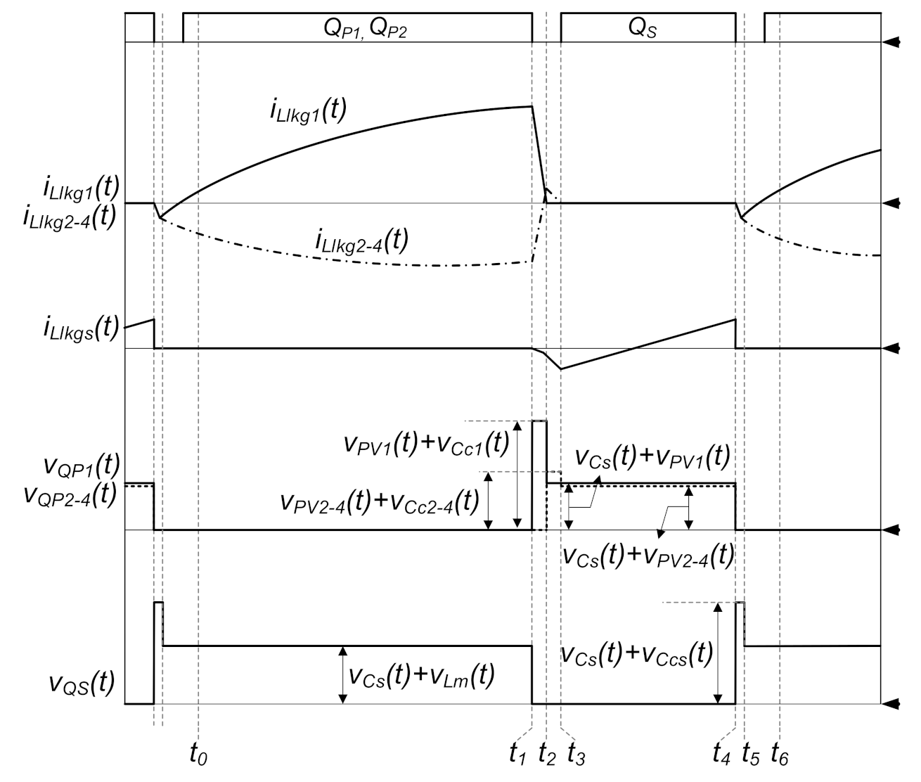
2.2. Operation Principle of the Proposed DPP Converter

Figure 3 and Figure 4 illustrate the key waveforms and operational principle of the proposed converter. Furthermore, two PV submodules were configured and the analysis of the proposed DPP converter was performed with respect to six modes.
In addition, the following assumptions are made:
  • Power generation of the PV1 submodule is greater than that of the PV2 submodule due to shading and failure of the PV2 submodule (PPV1 > PPV2).
  • All leakage inductances of the integrated transformer are equal (Llkg1 = Llkg2 = Llkgs).
  • The capacitance of the secondary side IP port is large enough, and it is assumed to be a voltage source.
  • All transformer windings have the same number of turns (NP1:NP2:NS = 1:1:1).
As can be seen in Figure 3 and Figure 4, the primary side switches QP1 and QP2 are turned on and off at the same time, and switch QS operates opposite to QP1 and QP2. The operating waveforms in Figure 3 represent leakage inductor voltage vLlkg1(t), vLlkg2(t), magnetizing inductor voltage vLm(t), leakage inductor current iLlkg1(t), iLlkg2(t), magnetizing inductor current iLm(t), primary side the switch voltages vQP1(t), vQP2(t), the secondary side switch current iQS(t), and the secondary side switch voltage vQS(t) are shown, and the circuit in Figure 4 consists of the input and output capacitors CPV1, CPV2, and CS; leakage inductors Llkg1, Llkg2, and Llkgs; snubber resistors RC1, RC2, and RCS; snubber capacitors CC1, CC2, and CCs; snubber diodes DC1, DC2, and DCS; magnetizing inductor Lm, and 1:1:1 transformers.
Mode 1 (t0t1): Both QP1 and QP2 remain turned on, and the PV1 voltage (vPV1(t)) is greater than the PV2 voltage (vPV2(t)) as mentioned in the above assumptions. Therefore, the voltage applied to the Lm (vLm(t)) has a value between vPV1(t) and vPV2(t). As a result, the voltages of Llkg1 and Llkg2 are as shown below.
v L l k g 1 t = v P V 1 t v L m t ,
v L l k g 2 t = v P V 2 t v L m t ,
From (1) and (2), iLlkg1(t) increases and iLlkg2(t) decreases. For iLlkg2(t), since the transformer windings NP1 and NP2 are the same, it can be expressed as (3). Therefore, it can be seen that the current of the PV1 submodule flows to the PV2 submodule and vLm(t) can be obtained using (1)–(3) and represented as (4)
i L l k g 2 t = i L m t i L l k g 1 t ,
v L m t = v P V 1 t + v P V 2 t · L m L l k g + 2 L m ,
Mode 2 (t1t2): Both QP1 and QP2 are turned off, and the body diodes of QP2 and QS conduct. The magnetizing current iLm(t) decreases when an output voltage −VCs_IP · NP1/NS is applied at the primary side. The energy stored in the leakage inductor Llkg1 is consumed through an RCD snubber.
Mode 3 (t2t3): In Mode 2, both QP1 and QP2 maintain a turn-off state, while the primary and secondary sides of the PV2 submodule are commutated to reduce the current flowing through the primary side and increase the current flowing through the secondary. In addition, since the QS switch is turned off, the current flowing through the secondary side continues to flow through the body diode. At this time, the energy stored in Llkg2 is consumed by the RCD snubber. Since the voltage of the magnetizing inductor is −VCs_IP · NP1/NSVLlkgs(t), iLm(t) continues to decrease. Furthermore, the voltage, Llkg1 becomes zero, and therefore, iLlkg1 also remains zero.
Mode 4 (t3t4): In Mode 2 and Mode 3, ZVS is possible because the secondary side body diode conducted current. For Lm, since −VCs_IP · NP1/NS is reflected, the magnetizing current iLm(t) decreases from a positive value to a negative value, as shown in Figure 3. At the same time, at the secondary side, both charge and discharge occur, which, in turn, resets the transformer. As a result, the average value of the secondary side current becomes zero, and thus the magnetizing current offset becomes zero.
Mode 5 (t4t5): The QS switch is turned off, and the energy stored in the leakage inductance Llkgs is consumed by the RCD snubber resistance. At this time, the leakage inductor current is reflected to the primary side, resulting in commutation on the primary and secondary sides.
Mode 6 (t5t6): It starts when the primary and secondary sides commutation is finished. Since the voltages reflected to Llkg1 and Llkg2 are the same as (1) and (2), iLlkg1(t) increases and iLlkg2(t) decreases. In addition, since iLlkg1(t) and iLlkg2(t) are conducting through the switch body diode, ZVS turn-on is performed when both QP1 and QP2 are turned on.

3. Proposed DPP Converter Design Method

3.1. Bus Voltage and IP Port Voltage

The bus voltage of the proposed DPP converter is shown in Figure 2, and the PV submodules are connected in series, so the bus voltage can be represented by (5). The IP port voltage can be expressed as (6) because it is same as the input–output.
V B u s 4 · V P V , m o d u l e ,
V C s _ I P n D 1 D V P V , m o d u l e ,
where n = Ns/NP is the turn ratio.

3.2. Primary Side Current of the Proposed DPP Converter

Since the primary side current is same as the switch current, it is proportional to the switch turn-off loss and the RCD snubber loss. Figure 5 shows the equivalent circuit of the primary switch turned-on state when two PV submodules are connected in series. In this equivalent circuit the magnetizing inductor was ignored because the magnetizing inductance is much larger than the leakage inductance. In addition, since the leakage inductance is very small, it is simply shown in Figure 5 considering the wire resistance (Rwire) and the switch-on resistance (Rds(on)). The PV1 input capacitor voltage vCPV1(t) can be obtained through the equivalent circuit in Figure 5, and it can be expressed by (7) using a Laplace transformation. The voltage vCPV1(t) of the input capacitor can be obtained by the inverse Laplace transform of (7), and this is shown in (8).
V C P V 1 S = V C P V 1 0 S + 1 S C P V 1 R e q + S L e q + 1 S C e q × V C P V 2 0 S V C P V 1 0 S + L l k g 2 I L l k g 2 0 I L l k g 1 0 ,
v C P V 1 t = V C P V 1 0 + C e q C P V 1 × V C P V 1 0 V C P V 2 0 · e ω 2 Q t sin ( ω β t + θ ) β 1 + L l k g 2 I L l k g 2 0 L l k g 1 I L l k g 1 0 · ω β e ω 2 Q t sin ω β t ,
where Req is the equivalent resistance of Rwire and Rds(on), Leq is the equivalent leakage inductance of Llkg1 and Llkg2, and Ceq is the equivalent capacitance of CPV1 and CPV2, ω = 1 / L e q C e q , Q = L e q / R e q C e q , β = 1 1 / 4 Q 2 , θ = cos 1 1 / 2 Q , and vCPV1(0), vCPV2(0), iLlkg1(0), and iLlkg2(0) are the initial values. iLlkg1(t) can be obtained by (9)
i L l k g 1 t = C P V 1 d V C P V 1 t d t + I P V 1 , i n ,
where IPV1,in signifies the input current induced by the PV submodule. It can be seen that, in (9), the leakage inductor current is affected by a small variation in the input capacitor voltage. In addition, since a small voltage is applied to the leakage inductor because of the voltage of the equivalent resistor, the leakage inductor current performs a Quasi-resonance operation. Therefore, due to the Quasi-resonant leakage current, a low leakage current at switch turn-off can be achieved resulting in a low snubber loss and switch turn-off loss.

3.3. Switch Loss and RCD Snubber Loss of Proposed DPP Converter

The root-mean-square (RMS) currents at the primary and secondary sides of the DPP converter are shown in Table 1. The losses of the conventional flyback DPP converter and the proposed DPP converter are shown in Figure 6.
The RCD snubber design should set the RCD snubber capacitor voltage VCc in consideration of the switch voltage. In the case of the RCD snubber resistance, it can be obtained by (10)
1 2 L l k g × i L l k g 2 × f s = V C c 2 R C
As the frequency increaes, VCc increases, and the switch voltage rating should increase. That is, when desinging an RCD snubber, appropriate frequency selection is required. The proposed DPP converter can be obtained using the equivalent circuit of Figure 5.
The proposed DPP converter reduces the number of switches by integrating the secondary side. In addition, since the entire switch performs a ZVS turn on, as shown in Figure 4 and Figure 7, the switching loss of the proposed DPP converter is decreased. Figure 6 presents a loss analysis diagram and shows that the switching loss of the proposed DPP converter is smaller than that of the conventional flyback DPP converter. The switch loss can be obtained as [21,22]:
P Q o n = 0.5 V D S · I D S m i n · t o n · f S + V D S ·   f S × I D S m i n · t r r + Q r r ,
P Q o f f = 0.5 V D S · I D S m a x · t o f f · f S ,
P Q , c o s s = 0.5 C O S S · V D S 2 · f S ,
P Q , c o n d = R d s o n · I r m s 2 ,
For the conventional flyback DPP converter, the leakage inductance is larger than the proposed DPP converter because the number of windings is large. In addition, the RCD snubber loss increases due to large leakage inductance and large number of RCD snubbers. The RCD snubber loss of the proposed DPP converter is relatively low compared with that of the conventional converter. This is because a low leakage inductance is induced by a low turn-number of the integrated transformer, and a quasi-resonant leakage inductor current induces a small amount of energy in the leakage inductor at the switch turn-off instant.

3.4. Transformer Design and Loss

Table 2 shows the transformer area product (AP) values of the conventional flyback DPP converter and the proposed DPP converter. Since the transformer in a conventional DPP converter stores energy, a magnetizing current offset occurs. Therefore, the transformer should be designed with high number of transformer windings. As a result, not only would the volume of the transformer be large but also multiple transformers are required. This makes the size of the conventional DPP converter considerably large.
On the other hand, the proposed DPP converter stores and transmits energy through the leakage inductor. Thus, it is possible to reduce the number of windings by removing the magnetizing current offset and increasing flux variation of the transformer. As a result, despite the multi-winding structure of the integrated transformer, the proposed integrated transformer has a reduced volume of up to 44% of the multiple transformers in the conventional flyback DPP converter. The transformer AP of the proposed DPP converter can be expressed by (14) considering the number of multi-windings (Nmw) on the primary side in the transformer core window area (Aw).
A P = A e · A w = L m I L m , p e a k N P B m · N m w · I p , r m s N P + I s , r m s N s K u J .
A conventional flyback DPP converter uses four transformer cores, and even if core loss is small due to low peak-to-peak flux density (ΔB), the number of windings is large; thus, the conduction loss increases. By contrast, the proposed DPP converter comprises only one transformer, and even if the core loss increases due to the high ΔB, the conduction loss decreases, and therefore the transformer loss is lower than that of the conventional flyback DPP converter as shown in Figure 6.
Figure 8 shows the relationship between duty and loss when the magnetizing current is constant. As the duty increases, the conduction loss decreases and core loss increases. In addition, the total loss, which is the sum of the conduction loss and the core loss, becomes the smallest around 0.5 duty. Accordingly, the proposed DPP converter was designed to operate at about 0.5 duty.
In the proposed DPP converter, the volume of the transformer was reduced by removing the magnetizing current offset of the transformer despite the integration of multiple transformers. The number of components and volume of the transformer were also decreased by integrating the secondary side switches. Moreover, since all the switches perform ZVS turn on, the efficiency is improved by reducing the switching loss. Therefore, the proposed DPP converter is a promising converter in regard to its wide range of application, such as a battery cell balancing circuit and PV.

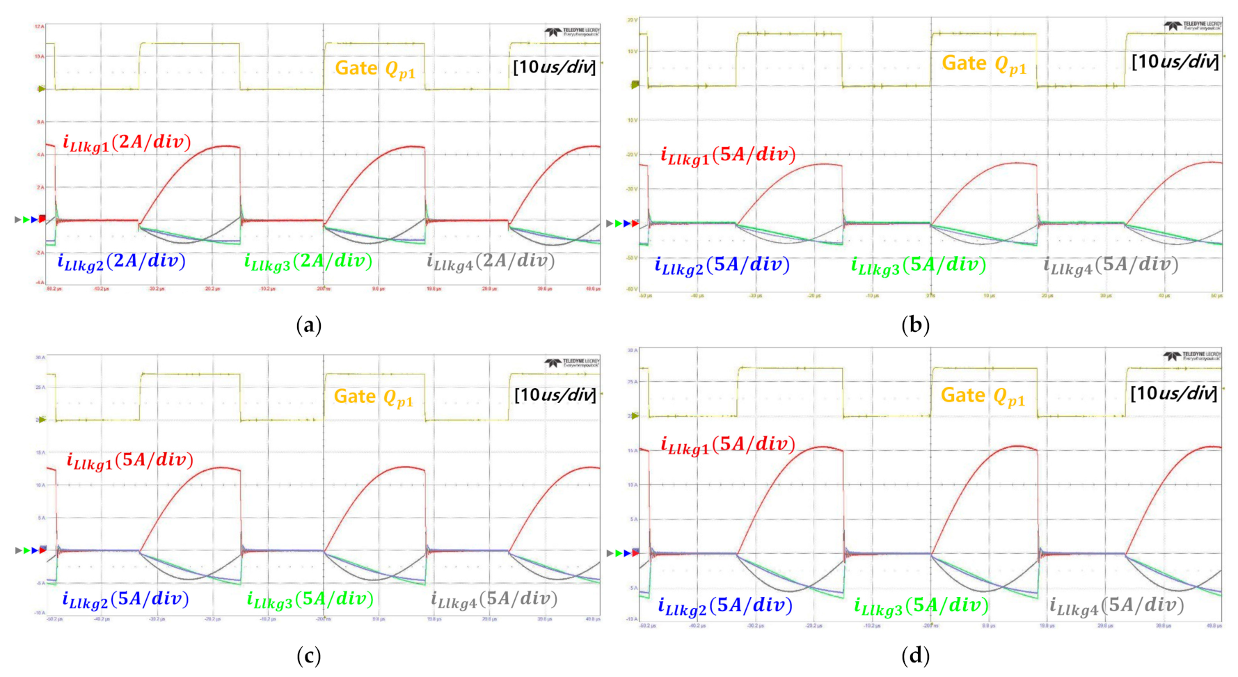
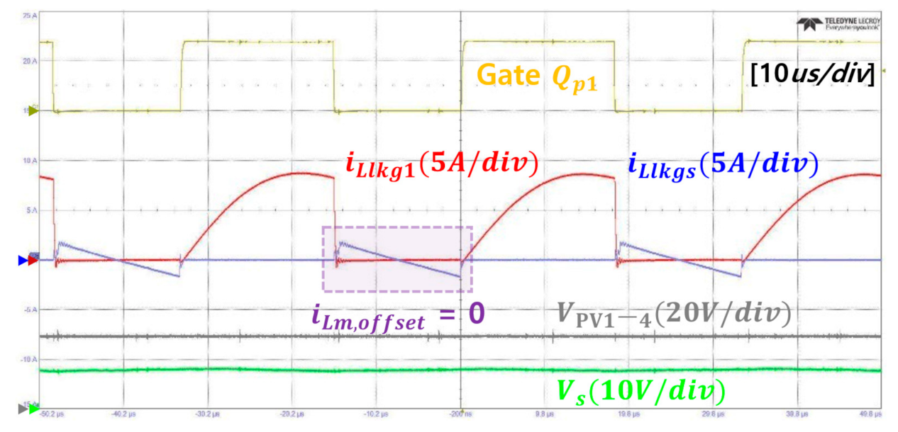
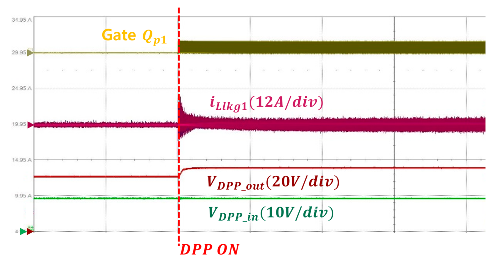
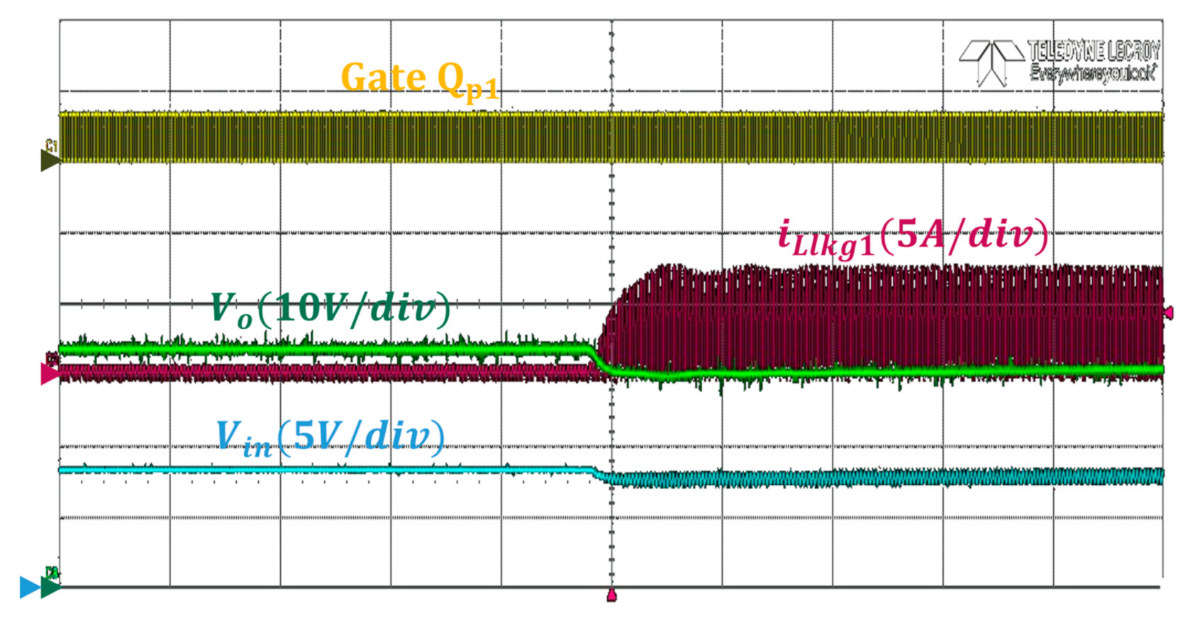
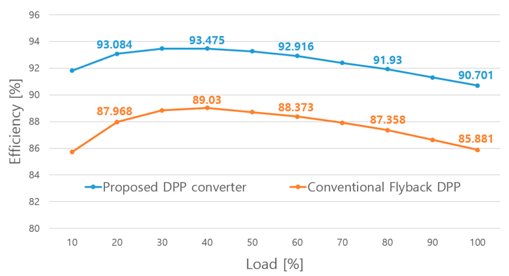
4. Experimental Results

The prototype was tested using power analyzer (WT5000), DC power supply (DSP1500WS), oscilloscope (WaveRunner 8058HD), and electronic load (PRODIGIT 34105A) and used the PV Simulator function of DC power supply.
Figure 9 illustrates a prototype of the proposed DPP converter, and it was built to solve the power imbalance when PV submodules are connected in series. The design specifications of the proposed and conventional flyback DPP converters are represented in Table 3 and Table 4. Table 4 represents conventional flyback specification, and since the switching frequency is larger than the proposed DPP converter, the transformer core volume may be designed to be smaller.
The proposed DPP converter was designed at 45 kHz, which further reduced the transformer volume. However, the snubber voltage and snubber loss are proportional to the frequency, and thus the switching frequency must be limited. The proposed converter as designed at 30 kHz to reduce snubber loss. Even if the switching frequency is designed to be 30 kHz, the transformer is small, and thus efficiency and power density can be simultaneously improved.
To verify the performance of the proposed converter, various experiments were conducted considering the worst-case condition as shown in Figure 10. The worst-case condition means that the PV1 submodule generates 60 W power while the other submodules generate 0 W. As a result, the DPP converter absorbs the 45 W surplus power from the PV1 submodule and supplies 15 W power to each submodule to mitigate the power imbalance among submodules.
Figure 11 shoes experimental waveforms of the proposed converter with respect to load variation. As shown in Figure 11, through the proposed DPP converter, the surplus current of the PV1 submodule is injected to other submodules to reduce the power difference. Meanwhile, as presented in Figure 7 and Figure 11, the deviation of the leakage inductor currents of submodules occur.
This is because the leakage inductor of the proposed DPP converter is too small; the small voltage variation in the leakage inductor, resulting from the input capacitor voltage ripple, leads to a large current variation similar to quasi-resonant current. Due to this quasi-resonant current, the switch turn-off current of the proposed converter can be reduced, which leads to small switching loss and snubber loss. Consequently, the proposed converter is able to provide high efficiency compared with the conventional DPP converter.
Figure 12 shows the magnetizing current waveform of integrated transformer. As shown in Figure 12, the magnetizing current shows zero offset current due to the current second balance of IP port capacitor, which signifies zero DC bias of the transformer.
Moreover, it is possible to design the integrated transformer with relatively large flux variation inducing low turn numbers compared with the conventional flyback DPP converter. Thus, in spite of primary multi-windings, the integrated transformer significantly reduces the volume of the magnetic components.
Figure 13 presents the ZVS characteristics of the proposed DPP converter under the worst-case conditions. Since the ripple of the magnetizing current is constant and the magnetizing current shows a zero offset, the conduction period of the body diode of the switch reduces as the load increases. Therefore, the 100% load condition is the worst-case condition for the ZVS operation. As represented in Figure 13, we confirmed that the ZVS performed well under full-load conditions, i.e., the worst-case conditions.
Figure 14 presents the voltages of the PV submodules before and after the DPP converter is used. Prior to the operation of the DPP converter, the input voltage was applied only to PV1. However, after complete operation of the DPP converter, the voltages of the PV submodules became balanced since the power difference between the submodules was mitigated.
Figure 15 shows the key waveform at the soft start-up region that can start the converter without excessive inrush current. It can be seen that the output voltage is charged compared with the proposed DPP converter through soft start up. As a result, it is possible to operate stably.
Figure 16 shows the load transient waveform. When partial shading occurs in the PV module, the dynamic of proposed converter can be checked.
Figure 17 shows the efficiencies of the proposed DPP converter and the conventional flyback DDP converter. It can be seen that the efficiency of the proposed DPP converter is about 5% higher than that of the conventional converter under entire load conditions. For the proposed DPP converter, more than 93% efficiency under 20–50% load and maximum 93.475% efficiency about 40% load were achieved. Since the proposed DPP converter provides high power density and efficiency, the DPP converter can be applied to various applications with power imbalance, such as a battery equalizer.

5. Conclusions

The current research developed a DPP converter with single multi-winding transformer by integrating multiple transformers and secondary sides of the conventional flyback DPP converter. The integrated transformer has a reduced volume and can maximize the power density because the magnetizing current offset is removed. Therefore, the proposed DPP converter can decrease both the conduction loss and core loss because of the zero magnetizing current offset and integrated transformer.
In addition, since ZVS is possible, the efficiency can be maximized. Moreover, since the gate signal of the primary side switch is driven by a single PWM signal, the control and driving circuits can be simplified. Therefore, the proposed converter is suiFigure for a DPP converter and can be applicable to battery balancing circuits. In the future, we plan to conduct research that further optimizes the power density eliminating the secondary side and using a planar transformer instead of a PQ core.

Author Contributions

Conceptualization, J.-H.L. and H.-S.Y.; Data curation, J.-H.L., D.-I.L., Y.-J.H. and H.-S.Y.; Formal analysis, J.-H.L., D.-I.L., Y.-J.H. and H.-S.Y.; Project administration, J.-H.C.; Supervision, J.-H.C. and H.-S.Y.; Writin—original draft, J.-H.L. and H.-S.Y.; Writing—review & editing, J.-H.L. and H.-S.Y. All authors have read and agreed to the published version of the manuscript.

Funding

Research Assistance Program (2021) of Incheon National University. National Research Foundation of Korea: NRF-2020R1C1C1010268.

Acknowledgments

This work was supported by Research Assistance Program (2021) of Incheon National University. This work was supported by the National Research Foundation of Korea (NRF) grant funded by the Korea government (MSIT) (NRF-2020R1C1C1010268).

Conflicts of Interest

The authors declare no conflict of interest.

References

  1. Chmielewski, A.; Szulim, P.; Gregorczyk, M.; Gumiński, R.; Mydłowski, T.; Mączak, J. Model of an electric vehicle powered by a PV cell—A case study. In Proceedings of the 2017 22nd International Conference on Methods and Models in Automation and Robotics (MMAR), Miedzyzdrije, Poland, 28–31 August 2017; pp. 1009–1014. [Google Scholar]
  2. Mäki, A.; Valkealahti, S. Power Losses in Long String and Parallel-Connected Short Strings of Series-Connected Silicon-Based Photovoltaic Modules Due to Partial Shading Conditions. IEEE Trans. Energy Convers. 2012, 27, 173–183. [Google Scholar] [CrossRef]
  3. Winston, D.P. Efficient Output Power Enhancement and Protection Technique for Hot Spotted Solar Photovoltaic Modules. IEEE Trans. Device Mater. Rel. 2019, 19, 664–670. [Google Scholar] [CrossRef]
  4. Chen, S.M.; Liang, T.J.; Hu, K.R. Design, analysis, and implementation of solar power optimizer for DC distribution system. IEEE Trans. Power Electron. 2013, 28, 1764–1772. [Google Scholar] [CrossRef]
  5. Kim, N.; Parkhideh, B. PV-battery series inverter architecture: A solar inverter for seamless battery integration with partial power dc-dc optimizer. IEEE Trans. Energy Convers. 2018, 34, 478–485. [Google Scholar] [CrossRef]
  6. Walker, G.R.; Sernia, P.C. Cascaded dc-dc converter connection of photovoltaic modules. Proc. IEEE Power Electron. Spec. Conf. 2022, 1, 24–29. [Google Scholar]
  7. Kashani, M.G.; Mobarrez, M.; Bhattacharya, S. Variable interleaving technique for photovoltaic cascaded DC–DC converters. In Proceedings of the 40th Annu. Conf. IEEE Ind. Electron. Soc. (IECON), Dallas, TX, USA, 29 October–1 November 2014; pp. 5612–5617. [Google Scholar]
  8. Khan, O.; Xiao, W. Review and qualitative analysis of submodule-level distributed power electronic solutions in PV power systems. Renew. Sustain. Energy Rev. 2017, 76, 516–528. [Google Scholar] [CrossRef]
  9. Olalla, C.; Hasan, M.N.; Deline, C.; Maksimovic, D. Mitigation of hot-spots in photovoltaic systems using distributed power electronics. Energies 2018, 11, 726. [Google Scholar] [CrossRef] [Green Version]
  10. Kim, K.A.; Shenoy, P.S.; Krein, P.T. Converter Rating Analysis for Photovoltaic Differential Power Processing Systems. IEEE Trans. Power Electron. 2015, 30, 1987–1997. [Google Scholar] [CrossRef]
  11. Jeong, H.; Cho, H.-T.; Kim, T.; Liu, Y.-C.; Kim, K.A. A scalable unit differential power processing system design for photovoltaic applications. In Proceedings of the IEEE Workshop Control Model Power Electron., Padova, Italy, 25–28 June 2018; pp. 1–8. [Google Scholar]
  12. Sun, K.; Qiu, Z.; Wu, H.; Xing, Y. Evaluation on High-Efficiency Thermoelectric Generation Systems Based on Differential Power Processing. IEEE Trans. Ind. Electron. 2018, 65, 699–708. [Google Scholar] [CrossRef]
  13. Jeon, Y.-T.; Park, J.-H. Unit-minimum least power point tracking for the optimization of photovoltaic differential power processing systems. IEEE Trans. Power Electron. 2019, 34, 311–324. [Google Scholar] [CrossRef]
  14. Ye, Z.; Wen, H.; Chu, G.; Li, X. Minimum-power-tracking for PV-PV differential power processing systems. In Proceedings of the 2017 IEEE 6th International Conference on Renewable Energy Research and Applications (ICRERA), San Diego, CA, USA, 5–8 November 2017; pp. 696–700. [Google Scholar]
  15. Shenoy, P.S.; Kim, K.A.; Johnson, B.B.; Krein, P.T. Differential power processing for increased energy production and reliability of photovoltaic systems. IEEE Trans. Power Electron. 2013, 28, 2968–2979. [Google Scholar] [CrossRef]
  16. Qin, S.; Cady, S.T.; Dominguez-Garcia, A.D.; Podgurski, R.C.N.P. A distributed approach to maximum power point tracking for photovoltaic submodule differential power processing. IEEE Trans. Power Electron. 2015, 30, 2024–2040. [Google Scholar] [CrossRef]
  17. Chu, G.; Wen, H. Design and Optimization of PV-Isolated-Port Photovoltaic Differential Power Porcessing System. In Proceedings of the 2018 IEEE International Conference on Power Electronics, Drives and Energy Systems (PEDES), Chennai, India, 18–21 December 2018; pp. 1–6. [Google Scholar]
  18. Olalla, C.; Deline, C.; Clement, D.; Levron, Y.; Rodriguez, M.; Maksimovic, D. Performance of power-limited differential power processing architectures in mismatched PV systems. IEEE Trans. Power Electron. 2015, 30, 618–631. [Google Scholar] [CrossRef]
  19. Jeong, H.; Lee, H.; Liu, Y.C.; Kim, K.A. Review of differential power processing converters techniques for photovoltaic applications. IEEE Trans. Energy Convers. 2019, 34, 351–360. [Google Scholar] [CrossRef]
  20. Jeon, Y.; Park, J.; Park, J. Differential Power Processing converter with cell balancing operation of multiple photovoltaic module systems. In Proceedings of the 2016 IEEE 8th International Power Electronics and Motion Control Conference (IPEMC-ECCE Asia), Hefei, China, 22–26 May 2016; pp. 736–740. [Google Scholar]
  21. Improving Efficiency of Synchronous Rectification by Analysis of the MOSFET Power Loss Mechanism. Available online: https://www.infineon.com/dgdl/Infineon-MOSFET_OptiMOS_improving_efficiency_of_synchronous_rectification_by_analysis_of_the_MOSFET_power_loss_mechanism-AN-v03_00-EN.pdf?fileId=db3a304320d39d590121a671f2d90c38 (accessed on 10 January 2022).
  22. Simple Design Techniques for Optimizing Efficiency and Efficiency and Overvoltage Spike of Synchronous Rectification in DC to DC Converters. Available online: https://www.infineon.com/dgdl/Infineon-MOSFET_OptiMOS_simple_design_techniques_for_optimizing_synchronous_rectification-AN-v01_00-EN.pdf?fileId=db3a304328c6bd5c0128da4cf0102cfe (accessed on 10 January 2022).
Figure 1. A conventional flyback Differential Power Processing converter (a) architecture and (b) circuit diagram.
Energies 15 01210 g001
Figure 2. Circuit configuration of the proposed Differential Power Processing converter.
Energies 15 01210 g002
Figure 3. Operational key waveforms of the DPP.
Energies 15 01210 g003
Figure 4. Operational mode of the DPP. (a) Mode 1 (t0t1). (b) Mode 2 (t1t2). (c) Mode 3 (t2t3). (d) Mode 4 (t3t4). (e) Mode 5 (t4t5). (f) Mode 6 (t5t6).
Energies 15 01210 g004
Figure 5. Equivalent circuit for the primary side turned-on state.
Energies 15 01210 g005
Figure 6. Loss analysis and comparison. (a) Switch, RCD snubber and transformer. (b) Conventional flyback DPP converter. (c) Proposed DPP converter. (d) Transformer.
Energies 15 01210 g006
Figure 7. Leakage inductor current and switch voltage waveforms.
Energies 15 01210 g007
Figure 8. Variation of Loss with duty.
Energies 15 01210 g008
Figure 9. The experimental prototype.
Energies 15 01210 g009
Figure 10. (a) Power flowchart of the proposed DPP converter. (b) Power flowchart of a conventional flyback DPP converter.
Energies 15 01210 g010
Figure 11. Experimental key waveform at 8 V input, 30 V output. (a) 20% load. (b) 50% load. (c) 80% load. (d) 100% load conditions.
Energies 15 01210 g011
Figure 12. Experimental key waveform of the magnetizing current of an integrated transformer.
Energies 15 01210 g012
Figure 13. ZVS waveform under 100% load conditions.
Energies 15 01210 g013
Figure 14. Experimental key waveform of submodule voltage with respect to the DPP operation.
Energies 15 01210 g014
Figure 15. Experimental key waveform of the DPP converter at the soft-start-up region.
Energies 15 01210 g015
Figure 16. Experimental key waveform of the DPP converter at the load transition.
Energies 15 01210 g016
Figure 17. Variation of measured efficiency with a load for 8 V input and 30 V output.
Energies 15 01210 g017
Table 1. RMS current of primary and secondary side of DPP converter.
ParameterConventional Flyback DPP Converter
IP,rms_PV17.78 A
IP,rms_PV2–42.73 A
IS,rms_PV15.51 A
IS,rms_PV2–41.93 A
ParameterProposed DPP Converter
IP,rms_PV18.49 A
IP,rms_PV2–42.7 A
IS,rms1.03 A
Table 2. Transformer AP.
ParameterConventional Flyback DPP Converter
AP13,736 mm4
Total AP54,944 mm4
ParameterProposed DPP Converter
AP24,085.6 mm4
Table 3. Proposed DPP converter parameters.
ParameterValue
Input voltage8 V
Output voltage30 V, 45 W
Switching frequency fs30 kHz
Transformer CorePQ3230
Turn ratio N P : N P n : N s 4:4:4
Magnetizing inductance L m 30 uH
Pri leakage inductance L l k g p 0.42 uH
Sec leakage inductance L l k g s 0.3 uH
Primary winding0.1 Φ/200 strands
Secondary winding0.5 Φ
RCD snubber resistance R C 2 kΩ
RCD snubber DiodeNRVTSA3100ET3G
Switch QIPD054N08
Hall SensorACS730KLCLU-30AB-T
Table 4. Conventional flyback DPP converter parameters.
ParameterValue
Input voltage8 V
Output voltage12 V, 45 W
Switching frequency fs45 kHz
Transformer CorePQ3220
Turn ratio N P : N P n : N s 6:8
Magnetizing inductance L m 22.2 uH
Pri leakage inductance L l k g p 0.378 uH
Sec leakage inductance L l k g s 0.669 uH
Primary winding0.1 Φ/160 strands
Secondary winding0.1 Φ/120 strands
RCD snubber resistance R C 1.1 kΩ
Switch QIPP057N08N3G
Publisher’s Note: MDPI stays neutral with regard to jurisdictional claims in published maps and institutional affiliations.

