Review

Comparative Study of DC-DC Converters for Solar PV with Microgrid Applications

by
Ingilala Jagadeesh
and
Vairavasundaram Indragandhi
*
School of Electrical Engineering, Vellore Institute of Technology, Vellore 632014, India
*
Author to whom correspondence should be addressed.
Energies 2022, 15(20), 7569; https://doi.org/10.3390/en15207569
Submission received: 29 August 2022 / Revised: 30 September 2022 / Accepted: 10 October 2022 / Published: 13 October 2022
(This article belongs to the Special Issue Smart Energy Management for Microgrid and Photovoltaic Systems)

Abstract

:
This review emphasizes the role and performance of versatile DC-DC converters in AC/DC and Hybrid microgrid applications, especially when solar (photo voltaic) PV is the major source. Here, the various converter topologies are compared with regard to voltage gain, component count, voltage stress, and soft switching. This study suggests the suitability of the converter based on the source type. The merits of a coupled inductor and interleaved converters in micro gird applications are elucidated. The efficiency and operating frequencies of converts for different operating modes are presented to determine the suitable converters for inductive and resistive loads. The drawbacks of converters are discussed. Finally, the mode of operation of different converts with different grid power sources and its stability and reliability issues are highlighted. In addition, the significance of the converter’s size and cost-effectiveness when choosing various PV source applications are discussed.

1. Introduction

The DC microgrid contains renewable energy sources and a hybrid energy storage unit. Hence, we are using Energy Management Methods to reduce power fluctuation on power quality [1]. We utilise many switching devices in renewable energy sources because high penetration occurs and switching losses or harmonics impact the utility grid’s system reliability [2]. This paper presents an overview of microgrids’ energy management strategies and grid integration technologies. To produce a clean energy future and minimize costs, renewable energy-based distributed generation is moving fast to meet the world’s vital needs of utilizing clean energy sources [3]. By converting solar energy into electrical energy without environmental contamination photovoltaic system provides a direct method. PV systems convert solar power to electric power integrated with the grid if it meets the grid code [4]. The DC microgrid consists of a battery energy storage system, wind turbine, grid-connected converter system, and dc loads. Solar PV is one of the renewable energy technologies best suited for islands, hills, and forest areas such as,
Minimal communication and transportation facilities.
Illiterate and Poor technical knowledge places.
Here power electronics blocks are required for grid integration to maximize the benefits of solar energy [5].
Solar PV and load require a suitable DC-DC converter to increase the system’s efficiency. Multiple converters are typically designed for high voltage gain of solar PV applications [6]. In addition, better dynamic response and less ripple are obtained by multiphase interleaved DC-DC converters, preserving their efficiency. This study presents a SEPIC, CUK combination converter-based interleaved converter for connecting distributed generation to bipolar DC micro grids and power architecture [7]. Finally, switched inductors and switched capacitors are used to provide a high gain. All semiconductor devices have the same voltage stress. Therefore, it is possible to utilize devices with uniform ratings and minimal internal resistance [8]. Finally, a multi-port isolated DC-DC converter replaced the traditional Buck/Boost circuit to ensure electrical isolation of the energy storage system’s micro sources [9]. The boost DC-DC converter topology has the following demerits: large capacitors are needed, there is a <4:1 voltage gain, parallel devices are required at high power levels, and there is a high ripple rate [10,11]. Due to their high conversion efficiency, minimal size, and low production costs, the described DC-DC converter topology a significant role in the power-generating industry, including microgrids. The DC-DC converters in are separated into isolated and non-isolated topologies [12,13]. The general classification of DC-DC converters are depicted in Figure 1.
When the traditional boost converter is preferred in PV systems, it has to be operated at a duty cycle of 0.88, making it difficult in practical application due to the limitation of semiconductor devices. Moreover, the boost converters suffer the drawback of high switching voltage stress and reverse recovery issues [14]. The applications of smart grid system are summarized in Figure 2.
The grid functions today are the same as when there were minor improvements, and the energy cost was relatively low. There is currently no heavy electricity storage technology available. Therefore, if we use this power during off-peak hours, we will build an effective system. However, we may adjust load consumption to increase grid efficiency, which is how the Smart grid differs from a traditional grid.
These converters require a higher power transformer, as higher power converters cannot use a single switch topology. For example, Half-bridge, push-pull and Full-bridge converters comes under another DC-DC isolated converters which use a minimum of multi-switch. Figure 3 represents a simplified hybrid microgrid charging station for battery-powered electric vehicles.
The PV technologies can be employed in various applications, including electric vehicles, domestic, and microgrid applications [15]. The different operating voltages of the DC-DC converters linked to the PV system are described. In addition, in grid-connected mode converters, suitable load types are identified along with their corresponding voltage gain and conversion efficiency. This review elucidates the operation of 14 types of DC-DC converters for grid-connected PV applications. This is followed by comparing the converters performance for different grid-connected PV systems operating modes along with discussed distributed energy sources. At last, each converters parametric analysis and components sizing comparison are critically examined to further identify the drawbacks in each converter for a particular source application for a specific mode of operation.

2. Requirements for the Selection of DC-DC Converter Topology

The DC-DC converter topologies that are to be used in a PV-based power supply should meet the conditions given in the subsequent paragraphs. A typical layout of DC microgid is depicted in Figure 4. Without increasing the stack size, we can obtain the desired DC voltage value with the help of the DC-DC converter. For example, the DC output from the polymer electrolyte membrane (PEM) FC stack is mostly around several tens of volts. Therefore, the ripple current value observed across the PV due to the DC-DC converter switching should be low. Most importantly, a sharp rise or a fall in the current and high-frequency current ripple of a large magnitude should be avoided [16].
An overview of the present-day technology in isolated DC-DC converters for PV-based power generation is presented in Table 1. The study includes an analysis of literature to understand current achievements and viewpoints. While many papers on the subject have been published, many of them do not include details on the achieved efficiency or the complexity of the converter when operating a greater number of devices, and issues with power density maximization are mentioned. Within the limited information available, a comparison of published literature for high voltage gain DC-DC converters is attempted, and an overview of each solution is provided.

3. Survey of DC-DC Converter Topologies

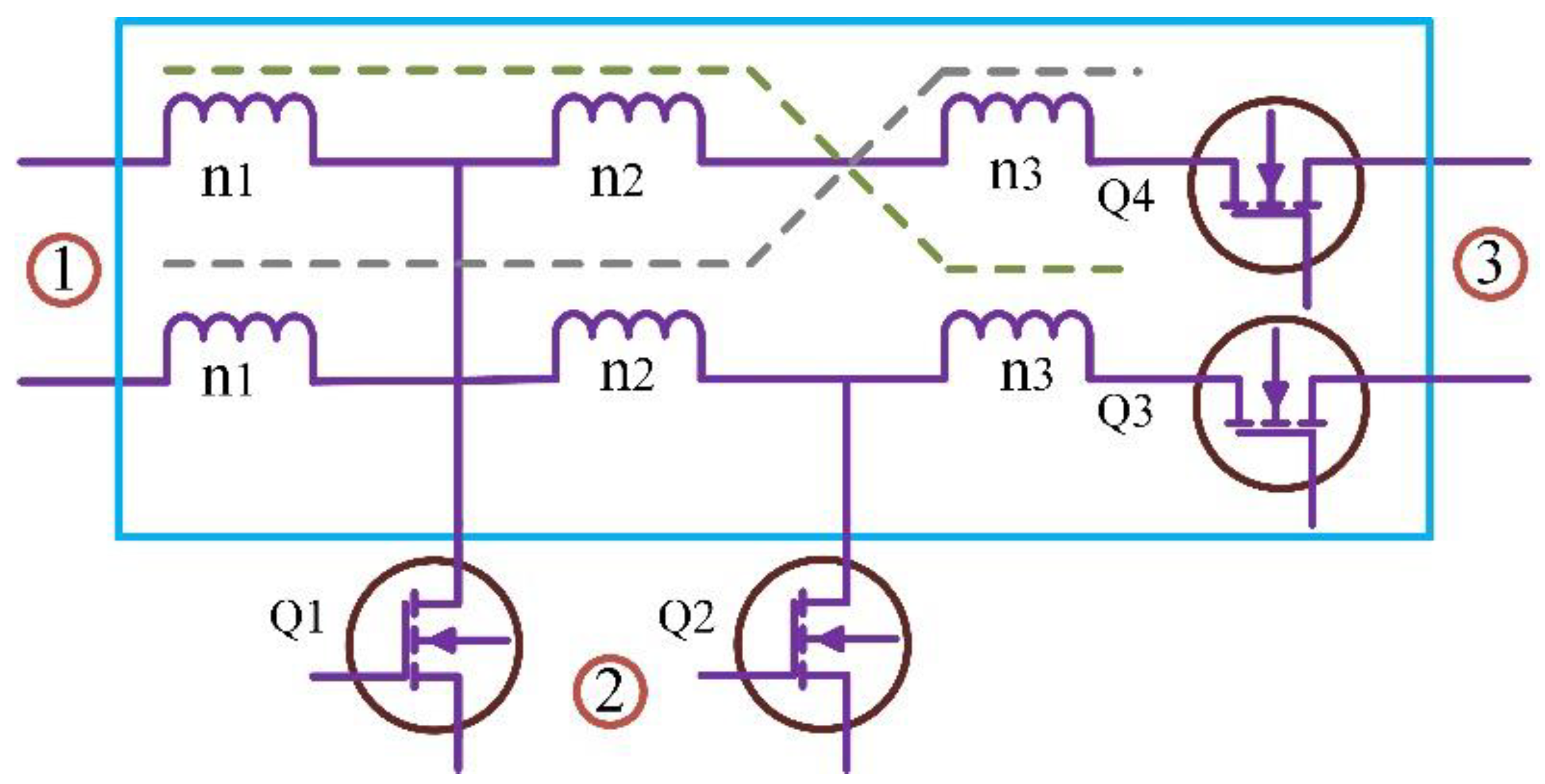
3.1. Coupled Inductor Converter Topology

This section enumerates the published solutions of coupled inductor topology DC-DC converters possess high gain, as shown in Figure 5, Figure 6, Figure 7 and Figure 8. Each published technique explains the topology used, the converter Vin and Vout range, and the power range of the experimental setup are given to validate the interfacing with FC for power generation. In [17] the authors proposed a DC-DC converter with soft switching exhibits continuous input current and a high voltage gain. Experimentally, a 200 W prototype having Vin = 24 V, and Vout = 360 V gives 96.4% efficiency at full load. The advantages of derived interleaved boost converter having Winding-Cross-Coupled Inductors (WCCIs) and passive-lossless clamp circuits are increased voltage gain, reduced switching voltage stress, and reduced reverse recovery problem due to the leakage inductance when compared with conventional interleaved boost converters [18]. An interleaved boost converter rated 1 kW, 40 V to 380 V experimental findings show an efficiency of 90.7% at full load, which is 5% better than a typical interleaved boost converter. [19]. A three-winding coupled inductor produced a high voltage gain. The energy in the leakage inductor is released to the output directly, reducing the switch stress. The output diode’s reverse recovery current is evaluated using a coupled inductor. A closed loop control method is used, which overcomes the power source voltage drift problem. The converter is used with a FC which gives a Po = 300 W Vout = 400 V, Vin = 27 V–36.5 V and Fs = 100 kHz. It gives a maximum efficiency of 95.2% at 220 W. A 200 W boost converter having coupled inductors, and buck-boost active clamps for low Vin applications is proposed in [20]. The Vin range is 25–40 V, Vout is 200 V and output current of 1A with a switching frequency of 66 kHz. ZVS turns on the main and auxiliary switches, and the boost diode is turned on DC-DC ZCS. Thus, the switching losses are chopped. The converter efficiency is 92%, and the output power is 200 W. A high voltage gains 250 W non-isolated DC-DC converter having a three-stage switching cell and voltage multiplier is proposed and demonstrates the Vin range is 30–45 V, and Vout is 400 V. The three-stage switching cells reduce the converter’s size and conduction losses while efficiency is 97% [20].
A high step-up DC-DC converter is required to boost the voltage value generated through the 400 V DC bus voltage PV. Passive loss clamped technology is used to improve efficiency and limit voltage stress. Recycling of leakage energy is possible with the help of passive losses clamped technology. The basic boost converters’ main disadvantages include problems with the electromagnetic interface, high voltage stress and hard switching on the semiconductor elements [21]. Coupled inductor DC-DC buck-boost converter is used for a step up and down by non-inverting voltage, this also offers high efficiency, control and regulation of input and output currents smoothly and immediately [22].
Table 1. Hybrid converters with observations.
RefType of ASDConverter TypeSupply DirectionObservations
[22]SupercapacitorBuck-boostBuck-boostThe construction and design are simple, using the same modules for all the positions in the system.
[23]Supercapacitor
and Batteries
Buck-boostBidirectional
buck-boost
The buck and boost modes of operation in the buck-boost converter connected with an FC, the operational dead-zone description, is not present in the system. It also consists of a design with complex control
[24]SupercapacitorBoostBidirectional
buck-boost
The experimental result of the boost converter is not present in the system, and the converter also has some start-up problems.
[25]SupercapacitorBoostBidirectional
buck-boost
The experimental load transient results of the boost converter are not present, and the converter has start-up problems.
[26]SupercapacitorBoostBidirectional
buck-boost
The converter consists of a design with complex control, and the converter has start-up problems.
[27]SupercapacitorBoostBidirectional
buck-boost
The boost converter consists of a design with complex control, and the converter has start-up problems.
The structure of the DC-DC boost converter consists of two hybrid, multiple voltage cells, and three winding coupled inductors. Using two multiple voltage cells, parallelly charged and discharged series, can provide very high voltage gain under the appropriate turns of ratio and duty cycle [28].

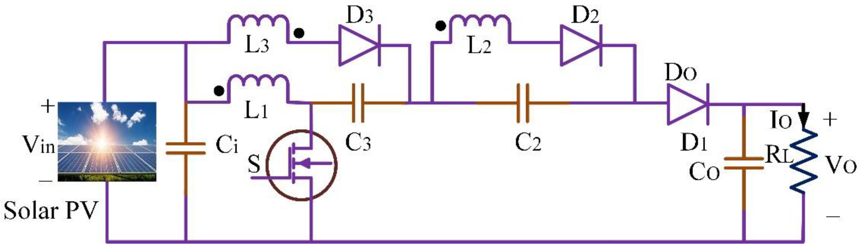
3.2. Interleaved Non-Isolated Topology

This section listed the published solutions of high gain interleaved non-isolated DC-DC converter topology. The voltage multiplier technique is used to the non-isolated DC-DC converters to possess a high step-up static gain, is presented in [29]. The Vin is 24 V, and the output Vout is 400 V. The output power is 400 W. The converter operated with a switching frequency of 40 kHz. The converter efficiency was 95%. Low electromagnetic interference production and commutation losses are attained. Without a power transformer, high static gain operation is possible. The Vin is 48 V and Vout is 380 V with an operating frequency of 100 kHz. The measured efficiency at 1 kW is 94.1%. The voltage doubler circuits increase the operating range of the converter by reducing the transformer’s parasitic capacitor’s effects. The interleaved Inductor-Inductor-Capacitor (LLC) converter for high gain is shown in Figure 9. This converter operates in two modes: independently and simultaneously. At the same frequency, both the interleaving converters are operated in the simultaneous mode. The single converter only operates in the independent mode.
The wider Vout range is possible only with frequency control and combined mode changing [30]. The phase-shedding technique is used to improve the efficiency of the interleaved switched capacitor DC-DC converter. The high voltage gain is achieved in the converter with modular characteristics and an interleaved configuration [31]. Using the lower voltage rating, the MOSFETs in the converter reduce the conduction losses [32]. The typical schematic layout is shown in Figure 10.
All diodes and switches operate on ZVS and ZCS techniques in the interleaved full soft-switching DC-DC converter. To reduce the power loss and to increase the efficiency of the DC-DC converters, the ZVS and ZCS are used. Finally, the auxiliary circuit is placed out of the main power path to avoid the switches’ high current and voltage stress [33]. The schematic circuit diagram of interleaved high step-up converter is depicted in Figure 11. A highly efficient power system always insists a reliable DC-DC converter. An interleaved boost converter is required to convert the high-current low-voltage to low-current high-voltage.
Classical boost converter deemed to be less advance then interleaved boost converter which offers high efficiency, low input ripple current, fast transient response, high reliability and less electromagnetic emission. Interleaved boost converters are suitable for the design of a highly efficient FC power system. To improve the system efficiency three-phase directly coupled interleaved boost converter using CoolMOS transistor and silicon carbide diode is used. Analysis based on the performances of interleaved converters are summarized in Table 2.

3.3. Isolated Push-Pull Boost Converter

This section lists the published solutions of isolated push-pull boost converter topology for high-gain DC-DC converters [38]. The proposed converter is a push-pull type hard switched isolated boost converter. The proposed converter is implemented along with a voltage clamp circuit on the isolation transformer’s primary and secondary sides. After the front end, the push-pull converter H-bridge DC-AC converter follows. The range of converter input Vin is taken as 25–45 V and Vout as 350–400 V. For the 900 W power level, the maximum calculated efficiency is 91%. Utilizing the resonant converter gives an advantage of a 1.5 kW front-end converter for FC applications, which is presented in [39]. On the secondary side of isolation transformer, a voltage doubler concept was introduced to tune the current resonance to minimize the diode losses (recovery). Switching active clamp circuits’ blocking voltage is used on both sides to clamp the peak. The proposed converter follows with an H-bridge DC-AC converter. Overall, a calculated system efficiency of 92.5 % is achieved with an Vin range of 30 V and an Vout of 350 V for 700 W power level.

3.4. Fly Back Converter Topology

This section lists the published solutions of Fly-back converter topology for high-gain DC-DC converters as shown in Figure 12 and Figure 13. A 300 W isolated high step-up ratio DC-DC converter that uses a voltage multiplier on the secondary side and active clamp on the transformer main side is proposed in [40]. The Vin range is 25–35 V, and Vout is 400 V. The circulating current through the active clamp is reduced due to the resonant phases between transformer leakage inductances and diode parasitic capacitances, which also lowers the conduction losses.
The converter’s efficiency of 92% to 94% for the entire Vin range and 300 W output power. A 300 W high step-up ratio converter for low-voltage and high-current energy sources is proposed [41]. The clamping diode integrated with boost-flyback (IBF) topology that naturally clamps parasitic oscillations. Resonance caused by the parasitic components helps to increase the voltage gain. The Vin range is 25–35 V, and Vout is 400 V. Various parameter has been evaluated and summarized in Table 3 for various converters. A simple design of asymmetrical forward cells of stacked multiple output topology is depicted in Figure 14.
The converter efficiency is about 94% for a 100 kHz frequency of operation, and the output power is 300 W. The conventional isolated converter with N-outputs requires 2 N primary switches. The above circuit requires N + 1 primary switches to independently regulate the secondary side N output voltages [45].

3.5. Half Bridge Converter Topology

The concept of two inductor boost converters was introduced by [46]. The boost converter topology is the boost version of the abovementioned current double topology, also called the HY-Bridge rectifier. Many papers have already been published on the high-power low-Vin application of the two inductor boosts [46,47,48,49,50,51], representing some important works on this topic. Two inductor isolated boost converters are often referred to as half-bridge converters, as shown in Figure 15. A 1 kW isolated current fed half-bridge LLC resonant DC-DC converter of 24–28 V input and 400 V output was presented in [52]. An un-regulated LLC converter is implemented, which acts as isolated voltage amplifier having constant voltage gain. Experimental efficiency of 90.2 % was achieved with 24 volts input under full load conditions. The LLC converter has inherent bi-directional power flow capability. A 1.2 kW isolated current fed active clamped half-bridge circuit with a Vin range of 28–43 V and an output of 380 Volts is presented in [53]. The proposed converter in this paper is compared with the existing converter topologies. The converter also tested for high power rating, and overall efficiency of 94% was achieved with better component utilization. Here a 200 W active clamped L-L current fed half-bridge isolated DC-DC converter with a 22 V input and 350 V output. [54]. The topology shown in this study achieves a wide-ranged ZVS of primary side switches from full load to light load conditions. Moreover, the auxiliary active clamp circuit absorbs the turn-off voltage spikes and also assists in achieving soft switching of primary devices [55]. Represents a 1 kW modified isolated two-inductor boost by active clamping and reset. The two transformers integrated by the individual rectifiers are connected in parallel on the input and output sides. Triangular switch currents can be observed due to active clamping. The Vin range is 26–50 V. The obtained Vout is 400 V. At 600 W output power, the maximum efficiency value is 95.6%. For the measured efficiency, the Vin condition is not published. [56] have used a 1 kW two-inductor boost converter with an active clamping. The Vin is 48 V. The observed Vout is 350 V. At a power rating of 500 W, an approximate peak efficiency of 87% is observed. The efficiency value drops to 77% at 1 kW output. A full-bridge boost converter reports 6–10% less efficiency on a comparative basis. As a part of the two-stage DC-DC converter for FC applications, a 1 kW two-inductor boost stage is designed in [57] as depicted in Figure 16.
Ref. [50] represent a 1.5 kW bi-directional two-inductor boost for a bi-directional interface between a 28 V and a 270 V aircraft power bus. On the low voltage side, active clamping and the rest is used to clamp the switching overvoltage. The range is 22–32 V. At Vin = 32 V and 750 W output, a peak efficiency value of 96% is achieved in the boost mode. Efficiency drops below 89% at 22 Vin and 1.5 kW output. A typical layout of DC-DC dual active bridge converter is shown in Figure 17.
A current fed hybrid dual active bridge DC-DC converter reduces the input high-frequency ripple current. While Power MOSFETs are switched with the ZVS technique. Low-voltage FC power conditioning systems employ two active bridge converters. Four power MOSFETs ( T 1 , T 1 a , T 2 , and   T 2 a ) and two inductors L 1 and L2 make up the input side. S w 1 , S w 2 , S w 3 , and S w 4   are the four MOSFETs that make up the output side. The auxiliary half-bridge consists of S w 5 and S w 6 . The power MOSFETs and ( C d and C u ) capacitors make up the auxiliary half-bridge. The transformer T is used to link the input and output sides. Here, the ratio of the transformer turns to the leakage inductance L k is 1: n [58]

3.6. Full Bridge Converter Topology

This section listed the published solutions of full-bridge converter topology for high gain DC-DC converters, as shown in Figure 18. A 500 W current fed full bridge isolated ZVS active clamp full-bridge converter with 22 V input and 350 V output for FC applications is presented in [59]. This converter uses active clamp switch to clamp the voltage spikes across the full bridge switches in the turn-off mode. Moreover, this active clamp switch helps to achieve soft switching of primary side devices. For example, a 100 W full-bridge isolated ZVS DC-DC converter with an input range of 48 V and an output range of 380 V is presented in [60]. The proposed converter uses an integrated magnetic concept to utilize the transformer better. Though the converter is unsuitable for high power grid applications, soft switching is claimed for 100 kHz switching operation. A 1.2 kW current-fed full-bridge topology with an input of 30 V and an output of 600 V was observed. The presented converter topology uses the current fed full bridge topology for FC applications. Based on the theoretical limitations of transferrable power, the optimized converter is designed for the given specifications.
A 5 kW isolated full bridge topology is proposed to apply FC vehicles [60]. The voltage clamping concept was introduced using a passive circuit to clamp the primary side switch blocking voltage. The proposed converter was analysed with a 24 V input and an output of 300 V. The calculated efficiency at peak power was 94%. Limited design data are provided to validate the converter. A soft switched 1 kW full-bridge isolated converter is demonstrated in [61]. During the switching, an overlap period of slow resonant commutation is achieved with the proposed converter. For the primary side switches, ZCS turn-off and ZCS turn-on is achieved. With the Vin = 22–27 V, Vout = 1 kV, a peak efficiency of 88% was achieved with 22 V input. An isolated full bridge converter for a 1.4 kW power level is proposed with a resonant LC circuit [62]. The resonant circuit is formed by connecting resonant capacitors parallel to the primary side switches and the LC tank circuit, forming a complete resonant circuit. With a Vin of 100 V and an output of 374 V with a narrow band frequency regulation, the maximum efficiency achieved is 90%.

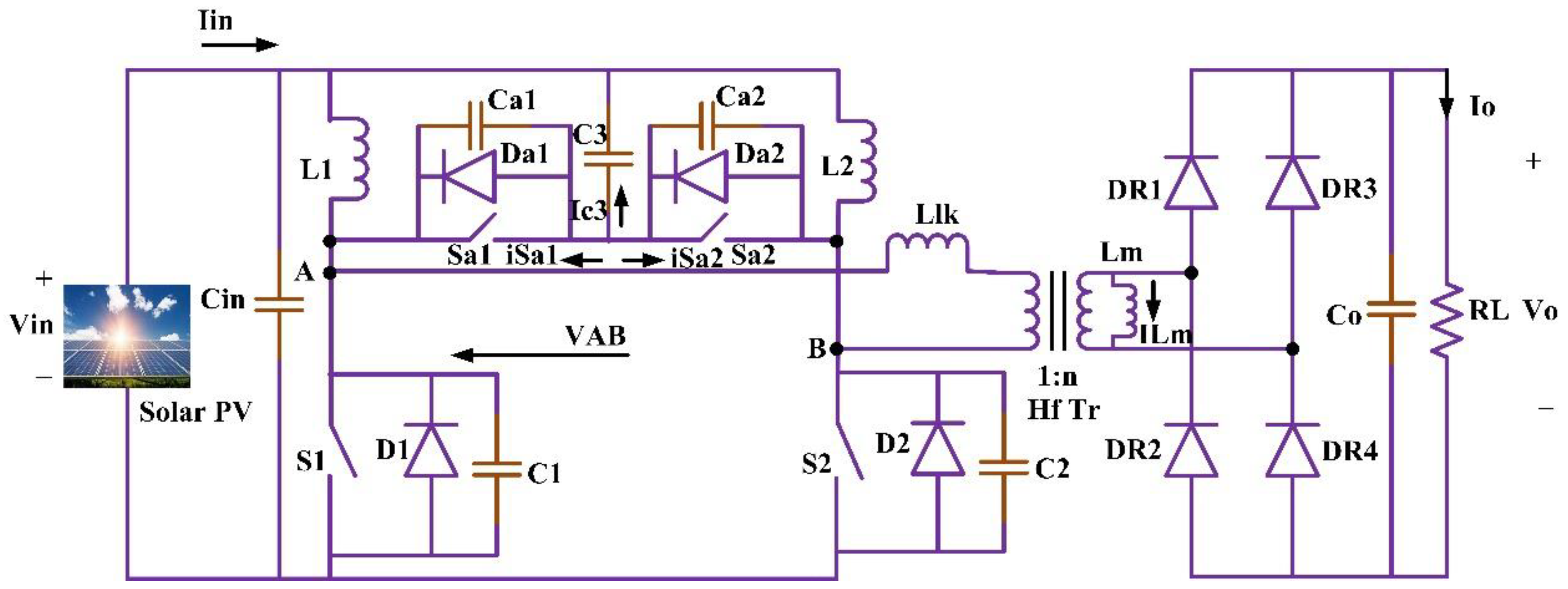
3.7. Resonant Converters

Below, Figure 19 shows the Series Resonant Converter topology (SRC). This paper [63] uses a parallel tank circuit formed by an (L-C)||L combination to achieve soft switching of high-frequency switches. The important feature of these converters including (1) Achieving an improved efficiency even at varying load and line conditions. (2) A wide range of soft switching ZVS can be achieved. (3) The Peak current capability of the switch varies with the input current variation and not with the load current changes.
Here Figure 20 shows is a full bridge phase shifted converter having an inductive output filter configuration. The Soft switched converter configuration for high-power applications vividly uses it. The proposed converter configuration uses a constant frequency capable of realizing ZVS of the main switches on the primary side with a minimal circulating circuit configuration. The ZVS is realized with a filter inductance, a leakage inductance of the transformer, a parasitic capacitance of the switches, and a snubber capacitance. The phase-shifted technique achieves control over the Vout with constant frequency. The important characteristics of the proposed converter include:
  • The duty cycle loss at the secondary side is a major limitation of this configuration.
  • A huge stress on the secondary side is rectifying diodes.
  • The parasitic ringing problem on the secondary side transformer.
  • For a wide range of ZVS, a large inductor is needed, but the transformer needs to decrease the Np/Ns ratio, which will increase the primary side current. Therefore, the conduction losses of the devices occur. A compromise between the Np/Ns ratio and inductor should be carried out to minimize the conduction losses of the active switches.

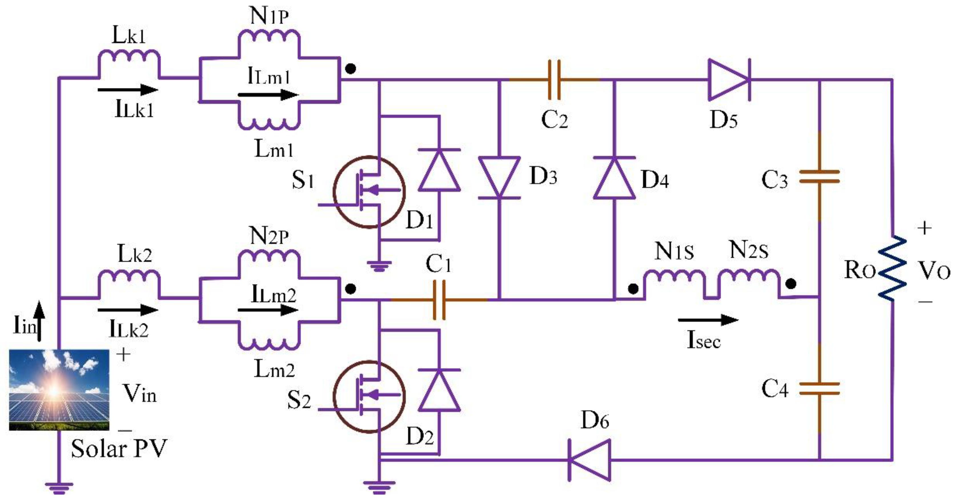
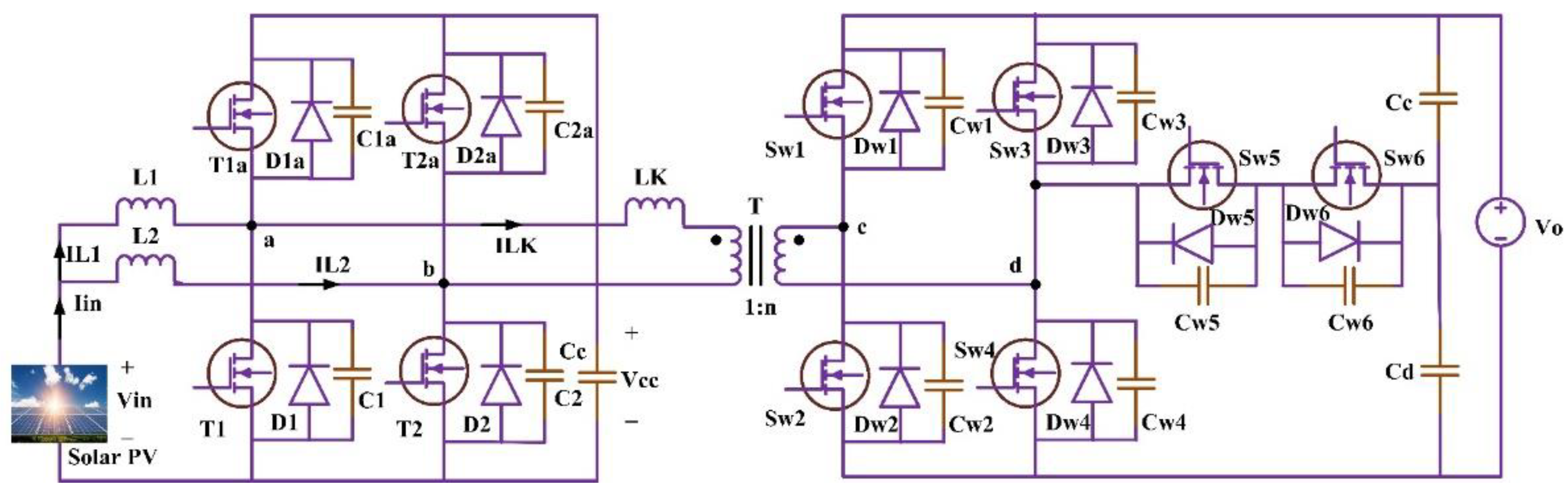
3.8. Interleaved Isolated Topology (ITLD Isolated Boost Converter)

A 200 W interleaved current fed ZVS active clamp full-bridge, and a Vout of 200 V is presented in [64]. The input current stress will be reduced due to interleaving and Vout extracted up to 700 V for three-phase grid-connected applications. A 1 kW interleaved current fed half-bridge topology with a Vin of 22–41 V and an output of 350 V is presented in [65]. The overall efficiency at full load achieved 92.8% with maximum converter utilization. The switching frequency is very low for the designed converter. Two current-fed full-bridge isolated converters are connected parallel to make an interleaved topology [66] and depicted in Figure 21. The voltage doubler circuit is connected in series to form a parallel input and a serial output configuration on the secondary side. The voltage clamping is carried out for the primary side switches using an active clamp circuit. With the Vin = 33 V, Vout = 400 V and the efficiency is 90.5% at 1.2 kW power levels.
The bidirectional isolated DC-DC converter technique reduces the input ripple current. The converter increases the conversion ratio and also the efficiency. Generally, a passive resistor capacitor-diode (RCD) snubber is required to store the energy in leakage inductance and clamp down the voltage spikes. Due to the use of the dual-inductor-capacitor-diode (LCD) snubber instead of the RCD snubber, the recycling of the leakage inductance, which is presented in the energy storing devices, is possible. Hence, the efficiency of the system increases [67].
Figure 22 shows the full bridge converter topology for high-gain DC-DC converters.

4. Summary of the Analysis

The comparison includes an analysis of high-gain converters meant for PV applications. The published performance details are provided in Table 4. It should be noted that the critical test conditions, such as Vin and Vout levels and the measurement tolerances, are usually not provided, making it difficult to compare the efficiency achieved wherever provided. The optimum comparison was achieved by considering 1. Worst-case efficiency, 2. The number of active devices, 3. Switching frequency, and 4. Size of the converter data. Beyond the performance data, the papers reveal an analysis of different types of converters. The boost converters do not deliver high step-up ratios efficiently in continuous conduction mode due to the switch’s high current and voltage stress and the diode reverse recovery loss. The non-isolated converter topologies are the suboptimal solution because it is directly connected to output high voltage side and the high boost ratios make it difficult to develop in non-isolated single-stage converter. The greater the differences in the voltage between the output of the FC (low voltage) and the DC link (high voltage), the greater there is need for electrical isolation between the two circuits [17,18,68]. Push-pull converters are typically unsuitable for FC power generation, especially at high power, due to the difficulty in overcoming transformer saturation [38,39]. The modified fly-back converters [69,70] suffer from voltage stress across the rectifier diode. The single winding carries a current, operates in a discontinuous mode (to avoid core saturation), and has high off-state voltage and poor core utilization. Current-fed full bridge converter operates at 10 kHz [66] (as it is a hard-switched converter), resulting in a larger converter due to the greater size of magnets and filters. The voltage clamping requirements [59] show that these circuits are necessary to reduce the switch stress. An active clamp (or reset) circuit requires greater switches and results in greater conduction losses due to the formation of the triangular current waveforms.
The comparison of measured efficiency in converter [18] and conventional boost converter is given in Figure 23. The conversion of 40 V to 380 V DC-DC gives the maximum efficiency of 92.6%.

5. Conclusions

This paper evaluates the 14 DC-DC boost converters’ efficiency, number of components, and stability. The significance of choosing a converter based on load and source requirements is evaluated. The importance of voltage gains and voltage stress factors when connecting solar PV to the grid is discussed. In addition to the non-isolated step up, interleaved and coupled inductors’ reliability with respect to solar PV system applications are outlined. The stress on the switches is reduced by coupled inductor with the ZVS operation system to reduce grid instability and synchronization drawbacks. Each converter importance is fully discussed in this review. Microgrids with solar PV will significantly increase the flexibility of the power system, but to make it reliable, it is necessary to choose the proper converters based on corresponding ratings. Selecting a suitable Converter linking PV source and Dc link bus enhances system performance. In addition, the bidirectional interleaved switched capacitor DC-DC converter implemented in grid connection helps reduction of capacitor voltage stress is discussed in this review. This further extends to by interleaved converter use in diminishing the current ripples at low voltage. Even though the converters pose the following merits, many constraints still need to be resolved, such as exceeding duty values to 50% and linear increases of switch voltage stress with increasing duty cycle.

Author Contributions

Implementation, Investigation, I.J.; Analysis, Supervision, Proofreading, V.I. All authors have read and agreed to the published version of the manuscript.

Funding

This research received no external funding.

Data Availability Statement

Not applicable.

Conflicts of Interest

The authors declare no conflict of interest.

References

  1. Sri Revathi, B.; Prabhakar, M. Solar PV Fed DC Microgrid: Applications, Converter Selection, Design and Testing. IEEE Access 2022, 10, 87227–87240. [Google Scholar] [CrossRef]
  2. Ahmad, J.; Zaid, M.; Sarwar, A.; Lin, C.H.; Asim, M.; Yadav, R.K.; Tariq, M.; Satpathi, K.; Alamri, B. A New High-Gain Dc-Dc Converter with Continuous Input Current for DC Microgrid Applications. Energies 2021, 14, 2629. [Google Scholar] [CrossRef]
  3. Ramesh, P.; Gouda, P.K.; Lakshmikhandan, K.; Ramanathan, G.; Bharatiraja, C. A Three Port Bidirectional DC-DC Converter for PV—Battery—DC Microgrid Application Using Fuzzy Logic Control. Mater. Today Proc. 2022, in press. [Google Scholar] [CrossRef]
  4. Zengin, S. A Hybrid Current Modulated DAB DC-DC Converter for Connecting PV Modules to DC Grid Considering Partial Shading. Comput. Electr. Eng. 2022, 101, 108109. [Google Scholar] [CrossRef]
  5. Mothilal Bhagavathy, S.; Pillai, G. PV Microgrid Design for Rural Electrification. Designs 2018, 2, 33. [Google Scholar] [CrossRef] [Green Version]
  6. Santosh Kumar Reddy, P.L.; Obulesu, Y.P. A Non-Cascading DC-DC Quadratic Boost Converter with High Voltage Gain for PV Applications. Int. J. Electron. 2022, 1–22. [Google Scholar] [CrossRef]
  7. Aranda, E.D.; Litran, S.P.; Prieto, M.B.F. Combination of Interleaved Single-Input Multiple-Output DC-DC Converters. CSEE J. Power Energy Syst. 2022, 8, 132–142. [Google Scholar] [CrossRef]
  8. Khan, S.; Zaid, M.; Mahmood, A.; Nooruddin, A.S.; Ahmad, J.; Alghaythi, M.L.; Alamri, B.; Tariq, M.; Sarwar, A.; Lin, C.H. A New Transformerless Ultra High Gain DC-DC Converter for DC Microgrid Application. IEEE Access 2021, 9, 124560–124582. [Google Scholar] [CrossRef]
  9. Liang, Y. Parallel Coordination Control of Multi-Port DC-DC Converter for Stand-Alone Photovoltaic-Energy Storage Systems. CPSS Trans. Power Electron. Appl. 2020, 5, 235–241. [Google Scholar] [CrossRef]
  10. Saravanakumar, T.; Saravana kumar, R. Design, Validation, and Economic Behavior of a Three-Phase Interleaved Step-Up DC–DC Converter for Electric Vehicle Application. Front. Energy Res. 2022, 10, 13081. [Google Scholar] [CrossRef]
  11. Saravanakumar, T.; Kumar, R.S. Fuzzy Based Interleaved Step-up Converter for Electric Vehicle. Intell. Autom. Soft Comput. 2023, 35, 1103–1118. [Google Scholar] [CrossRef]
  12. Arunkumari, T.; Indragandhi, V. An Overview of High Voltage Conversion Ratio DC-DC Converter Configurations Used in DC Micro-Grid Architectures. Renew. Sustain. Energy Rev. 2017, 77, 670–687. [Google Scholar] [CrossRef]
  13. Jagadeesh, I.; Indragandhi, V. A Novel PV Based High Voltage Gain Soft Switching DC—DC Boost Converter. Int. J. Eng. Technol. 2018, 7, 1034–1039. [Google Scholar] [CrossRef]
  14. Pan, C.T.; Lai, C.M. A High-Efficiency High Step-up Converter with Low Switch Voltage Stress for Fuel-Cell System Applications. IEEE Trans. Ind. Electron. 2010, 57, 1998–2006. [Google Scholar] [CrossRef]
  15. Kim, H.; Yoon, C.; Choi, S. An Improved Current-Fed ZVS Isolated Boost Converter for Fuel Cell Applications. IEEE Trans. Power Electron. 2010, 25, 2357–2364. [Google Scholar] [CrossRef]
  16. Rajashekara, K. Propulsion System Strategies for Fuel Cell Vehicles; SAE International: Warrendale PA, USA, 2000. [Google Scholar]
  17. Do, H.L. A Soft-Switching DC-DC Converter with High Voltage Gain. IEEE Trans. Power Electron. 2010, 25, 1193–1200. [Google Scholar] [CrossRef]
  18. Li, W.; He, X. A Family of Interleaved DC-DC Converters Deduced from a Basic Cell with Winding-Cross-Coupled Inductors (WCCIs) for High Step-Upor Step-down Conversions. IEEE Trans. Power Electron. 2008, 23, 1791–1801. [Google Scholar] [CrossRef]
  19. Wai, R.; Member, S.; Lin, C.; Duan, R.; Chang, Y. High-Efficiency DC-DC Converter With High Voltage Gain and Reduced Switch Stress. IEEE Trans. Ind. Electron. 2007, 54, 354–364. [Google Scholar] [CrossRef]
  20. Wu, T.; Member, S.; Lai, Y.; Hung, J.; Chen, Y.; Member, S. Boost Converter With Coupled Inductors and Buck—Boost Type of Active Clamp. IEEE Trans. Ind. Electron. 2008, 55, 154–162. [Google Scholar] [CrossRef]
  21. Molavi, N.; Adib, E.; Farzanehfard, H. Soft-Switched Non-Isolated High Step-up DC-DC Converter with Reduced Voltage Stress. IET Power Electron. 2016, 9, 1711–1718. [Google Scholar] [CrossRef]
  22. Ramírez-Murillo, H.; Restrepo, C.; Konjedic, T.; Calvente, J.; Romero, A.; Baier, C.R.; Giral, R. An Efficiency Comparison of Fuel-Cell Hybrid Systems Based on the Versatile Buck-Boost Converter. IEEE Trans. Power Electron. 2018, 33, 1237–1246. [Google Scholar] [CrossRef]
  23. Hilairet, M.; Béthoux, O.; Ghanes, M.; Tanasa, V.; Barbot, J.P.; Normand-Cyrot, M.D. Experimental Validation of a Sampled-Data Passivity-Based Controller for Coordination of Converters in a Fuel Cell System. IEEE Trans. Ind. Electron. 2015, 62, 5187–5194. [Google Scholar] [CrossRef]
  24. Thounthong, P.; Raël, S.; Davat, B. Control Strategy of Fuel Cell and Supercapacitors Association for a Distributed Generation System. IEEE Trans. Ind. Electron. 2007, 54, 3225–3233. [Google Scholar] [CrossRef]
  25. Hu, X.; Wang, J.; Li, L.; Li, Y. A Three-Winding Coupled-Inductor DC—DC Converter Topology With High Voltage Gain And. IEEE Trans. Power Electron. 2018, 33, 1453–1462. [Google Scholar] [CrossRef]
  26. El Fadil, H.; Giri, F.; Member, S.; Guerrero, J.M.; Member, S. Modeling and Nonlinear Control of a Fuel Cell/Supercapacitor Hybrid Energy Storage System for Electric Vehicles. IEEE Trans. Veh. Technol. 2014, 63, 3011–3018. [Google Scholar] [CrossRef] [Green Version]
  27. Vural, B.; Dusmez, S.; Uzunoglu, M.; Ugur, E.; Akin, B. Fuel Consumption Comparison of Different Battery/Ultracapacitor Hybridization Topologies for Fuel-Cell Vehicles on a Test Bench. IEEE J. Emerg. Sel. Top. Power Electron. 2014, 2, 552–561. [Google Scholar] [CrossRef]
  28. Tani, A.; Camara, M.B.; Dakyo, B. Energy Management Based on Frequency Approach for Hybrid Electric Vehicle Applications: Fuel-Cell/Lithium-Battery and Ultracapacitors. IEEE Trans. Veh. Technol. 2012, 61, 3375–3386. [Google Scholar] [CrossRef]
  29. Prudente, M.; Pfitscher, L.L.; Emmendoerfer, G.; Romaneli, E.F.; Gules, R. Voltage Multiplier Cells Applied to Non-Isolated DC-DC Converters. IEEE Trans. Power Electron. 2008, 23, 871–887. [Google Scholar] [CrossRef]
  30. Shahzad, M.I.; Iqbal, S.; Taib, S. Interleaved LLC Converter with Cascaded Voltage Doubler Rectifiers for Deeply Depleted PEV Battery Charging. IEEE Trans. Transp. Electrif. 2017, 4, 89–98. [Google Scholar] [CrossRef]
  31. Zhang, Y.; Gao, Y.; Li, J.; Sumner, M. Interleaved Switched-Capacitor Bidirectional DC-DC Converter with Wide Voltage-Gain Range for Energy Storage Systems. IEEE Trans. Power Electron. 2018, 33, 3852–3869. [Google Scholar] [CrossRef]
  32. Amiri, M.; Farzanehfard, H.; Adib, E. A Nonisolated Ultrahigh Step Down DC–DC Converter with Low Voltage Stress. IEEE Trans. Ind. Electron. 2018, 65, 1273–1280. [Google Scholar] [CrossRef]
  33. Bahrami, H.; Farhangi, S.; Iman-eini, H. A New Interleaved Coupled-Inductor Nonisolated Soft-Switching Bidirectional DC—DC Converter With High Voltage Gain Ratio. IEEE Trans. Ind. Electron. 2018, 65, 5529–5538. [Google Scholar] [CrossRef]
  34. Fekri, M.; Molavi, N.; Adib, E.; Farzanehfard, H. High Voltage Gain Interleaved DC-DC Converter with Minimum Current Ripple. IET Power Electron. 2017, 10, 1924–1931. [Google Scholar] [CrossRef]
  35. Nouri, T.; Hosseini, S.H.; Babaei, E.; Ebrahimi, J. Interleaved High Step-up DC-DC Converter Based on Three-Winding High-Frequency Coupled Inductor and Voltage Multiplier Cell. IET Power Electron. 2015, 8, 175–189. [Google Scholar] [CrossRef]
  36. Tseng, K.; Huang, C.; Shih, W. A High Step-Up Converter With a Voltage Multiplier Module for a Photovoltaic System. IEEE Trans. Power Electron. 2013, 28, 3047–3057. [Google Scholar] [CrossRef]
  37. Tseng, K.C.; Chen, J.Z.; Lin, J.T.; Huang, C.C.; Yen, T.H. High Step-up Interleaved Forward-Flyback Boost Converter with Three-Winding Coupled Inductors. IEEE Trans. Power Electron. 2015, 30, 4696–4703. [Google Scholar] [CrossRef]
  38. Andersen, G.K.; Klumpner, C.; Kjær, S.B.; Blaabjerg, F. A New Power Converter for Fuel Cells with High System Efficiency. Int. J. Electron. 2003, 90, 737–750. [Google Scholar] [CrossRef]
  39. Kwon, J.; Kim, E.; Kwon, B.; Nam, K. High-Efficiency Fuel Cell Power Conditioning System With Input Current Ripple Reduction. IEEE Trans. Ind. Electron. 2009, 56, 826–834. [Google Scholar] [CrossRef]
  40. Spiazzi, G.; Mattavelli, P.; Gazoli, J.R.; Magalhaes, R.; Frattini, G. Improved Integrated Boost-Flyback High Step-up Converter. In Proceedings of the IEEE International Conference on Industrial Technology, Via del Mar, Chile, 14–17 March 2010; pp. 1169–1174. [Google Scholar]
  41. Spiazzi, G.; Mattavelli, P.; Costabeber, A.; Member, S. High Step-Up Ratio Flyback Converter With Active Clamp and Voltage Multiplier. IEEE Trans. Power Electron. 2011, 26, 3205–3214. [Google Scholar] [CrossRef]
  42. Shitole, A.B.; Sathyan, S.; Suryawanshi, H.M.; Talapur, G.G.; Chaturvedi, P. Soft Switched High Voltage Gain Boost Integrated Flyback Converter Interfaced Single-Phase Grid Tied Inverter for SPV Integration. IEEE Trans. Ind. Appl. 2017, 54, 482–493. [Google Scholar] [CrossRef]
  43. Das, M.; Member, S.; Agarwal, V. Design and Analysis of a High Efficiency DC—DC Converter with Soft Switching Capability for Renewable Energy Applications Requiring High Voltage Gain. IEEE Trans. Ind. Electron. 2016, 63, 2936–2944. [Google Scholar] [CrossRef]
  44. Park, Y.; Jung, B.; Choi, S. Nonisolated ZVZCS Resonant PWM Dc-Dc Converter for High Step-up and High-Power Applications. IEEE Trans. Power Electron. 2012, 27, 3568–3575. [Google Scholar] [CrossRef]
  45. Chen, G.; Deng, Y.; Wang, K.; Hu, Y.; Jiang, L.; Wen, H.; He, X. Topology Derivation and Analysis of Integrated Multiple Output Isolated DC-DC Converters with Stacked Configuration for Low-Cost Applications. IEEE Trans. Circuits Syst. I Regul. Pap. 2017, 64, 2207–2218. [Google Scholar] [CrossRef]
  46. Wolfs, P.J. A Current-Sourced DC-DC Converter Derived via the Duality Principle from the Half-Bridge Converter. IEEE Trans. Ind. Electron. 1993, 40, 139–144. [Google Scholar] [CrossRef]
  47. Wen, J.; Jin, T.; Smedley, K. A New Interleaved Isolated Boost Converter for High Power Applications. In Proceedings of the Conference Proceedings—IEEE Applied Power Electronics Conference and Exposition—APEC, Dallas, TX, USA, 19–23 March 2006; Volume 2006, pp. 79–84. [Google Scholar]
  48. Attanasio, R.; Cacciato, M.; Gennaro, F.; Consoli, A. An Innovative Boost Converter for Fuel Cells Stationary Generation Systems. In Proceedings of the 30th Annual Conference of IEEE Industrial Electronics Society, Busan, Korea, 2–6 November 2004; pp. 2831–2836. [Google Scholar]
  49. Harfman Todorovic, M.; Palma, L.; Enjeti, P.N. Design of a Wide Input Range DC-DC Converter with a Robust Power Control Scheme Suitable for Fuel Cell Power Conversion. IEEE Trans. Ind. Electron. 2008, 55, 1247–1255. [Google Scholar] [CrossRef]
  50. Xiao, H.; Xie, S. A ZVS Bidirectional DC-DC Converter With Phase-Shift Plus PWM Control Scheme. IEEE Trans. Power Electron. 2008, 23, 813–823. [Google Scholar] [CrossRef]
  51. Liu, C.; Johnson, A.; Lai, J.S. A Novel Three-Phase High-Power Soft-Switched DC-DC Converter for Low-Voltage Fuel Cell Applications. IEEE Trans. Ind. Appl. 2005, 41, 1691–1697. [Google Scholar] [CrossRef]
  52. Lee, J.; Jeong, Y.; Han, B. An Isolated DC/DC Converter Using High-Frequency Unregulated LLC Resonant Converter for Fuel Cell Applications. IEEE Trans. Ind. Electron. 2011, 58, 2926–2934. [Google Scholar] [CrossRef]
  53. Jang, S.J.; Won, C.Y.; Lee, B.K.; Hur, J. Fuel Cell Generation System with a New Active Clamping Current-Fed Half-Bridge Converter. IEEE Trans. Energy Convers. 2007, 22, 332–340. [Google Scholar] [CrossRef]
  54. Rathore, A.K.; Bhat, A.K.S.; Oruganti, R. Analysis, Design and Experimental Results of Wide Range ZVS Active-Clamped L-L Type Current-Fed DC-DC Converter for Fuel Cells to Utility Interface. IEEE Trans. Ind. Electron. 2012, 59, 473–485. [Google Scholar] [CrossRef]
  55. Danyali, S.; Moradkhani, A.; Aazami, R.; Mejbel, M.T. New Dual-Source High-Gain ZVS DC-DC Converter for Integrating Renewable Power Source and Battery Storage. Electr. Power Syst. Res. 2022, 213, 108740. [Google Scholar] [CrossRef]
  56. Hadelu, L.M.; Noorpoor, A.; Boyaghchi, F.A.; Mirjalili, S. A New Molten Carbonate Fuel Cell Hybrid Power Generation System Using Two-Stage Sodium Thermo-Electrochemical Converter/Two-Stage Thermoelectric Generator: Performance Analysis and Multi-Objective Grasshopper Optimization. J. Power Sources 2022, 547, 232006. [Google Scholar] [CrossRef]
  57. Abdollahi Arjanaki, A.; Dehestani Kolagar, A.; Alizadeh Pahlavani, M.R. A Two-Level Power Management Strategy in a DC-Coupled Hybrid Microgrid Powered by Fuel Cell and Energy Storage Systems with Model Predictive Controlled Interface Converter. J. Energy Storage 2022, 52, 104861. [Google Scholar] [CrossRef]
  58. Sha, D.; Xu, Y.; Zhang, J.; Yan, Y. Current-Fed Hybrid Dual Active Bridge DC-DC Converter for a Fuel Cell Power Conditioning System With Reduced Input Current Ripple. IEEE Trans. Ind. Electron. 2017, 64, 6628–6638. [Google Scholar] [CrossRef]
  59. Prasanna, U.R.; Rathore, A.K. Analysis and Design of Zero-Voltage-Switching Current-Fed Isolated Full-Bridge Dc/Dc Converter. In Proceedings of the 2011 IEEE Ninth International Conference on Power Electronics and Drive Systems, Singapore, 5–8 December 2011; pp. 5–8. [Google Scholar]
  60. Jiang, X.; Wen, X.; Xu, H. Study on Isolated Boost Full Bridge Converter in FCEV. In Proceedings of the 7th International Power Engineering Conference, IPEC2005, Singapore, 29 November–2 December 2005; Volume 2005. [Google Scholar]
  61. Chen, R.Y.; Liang, T.J.; Chen, J.F.; Lin, R.L.; Tseng, K.C. Study and Implementation of a Current-Fed Full-Bridge Boost DC-DC Converter with Zero-Current Switching for High-Voltage Applications. IEEE Trans. Ind. Appl. 2008, 44, 1218–1226. [Google Scholar] [CrossRef]
  62. Jalbrzykowski, S.; Citko, T. Current-Fed Resonant Full-Bridge Boost DC/AC/DC Converter. IEEE Trans. Ind. Electron. 2008, 55, 1198–1205. [Google Scholar] [CrossRef]
  63. Rathore, A.K. Interleaved Soft-Switched Active-Clamped L-L Type Current-Fed Half-Bridge DC-DC Converter for Fuel Cell Applications. Int. J. Hydrogen Energy 2009, 34, 9802–9815. [Google Scholar] [CrossRef]
  64. Dharmesh, P.D.; Rathore, A.K. Interleaved Zero-Voltage-Switching Active-Clamped Current-Fed Full-Bridge Isolated Dc/Dc Converter for Fuel Cell Applications : A Case Study Analysis. In Proceedings of the 2012 IEEE Third International Conference on Sustainable Energy Technologies (ICSET), Kathmandu, Nepal, 24–27 September 2012; pp. 23–29. [Google Scholar]
  65. Reshma Gopi, R.; Sreejith, S. Converter Topologies in Photovoltaic Applications—A Review. Renew. Sustain. Energy Rev. 2018, 94, 1–14. [Google Scholar] [CrossRef]
  66. Kong, X.; Lim, T.C.; Khambadkone, A.M. Analysis and Control of Isolated Current-Fed Full Bridge Converter in Fuel Cell System. In Proceedings of the IECON Proceedings (Industrial Electronics Conference), Busan, Korea, 2–6 November 2004; Volume 3, pp. 2825–2830. [Google Scholar]
  67. Shen, C.L.; Liou, H.; Liang, T.C.; Gong, H.Z. An Isolated Bidirectional Interleaved Converter with Minimum Active Switches and High Conversion Ratio. IEEE Trans. Ind. Electron. 2018, 65, 2313–2321. [Google Scholar] [CrossRef]
  68. Aiswarya, P.; Varghese, B.M.; Joy, N.; George, A. Switched Inductor Based Bidirectional DC-DC Converter for High Voltage Gain. Mater. Today Proc. 2022, 58, 569–576. [Google Scholar] [CrossRef]
  69. Goudarzian, A.; Khosravi, A.; Ali Raeisi, H. Modeling, Design and Control of a Modified Flyback Converter with Ability of Right-Half-Plane Zero Alleviation in Continuous Conduction Mode. Eng. Sci. Technol. Int. J. 2022, 26, 101007. [Google Scholar] [CrossRef]
  70. Mirzaei, A.; Rezvanyvardom, M. High Voltage Gain Soft Switching Full Bridge Interleaved Flyback DC-DC Converter for PV Applications. Sol. Energy 2020, 196, 217–227. [Google Scholar] [CrossRef]
  71. Mumtaz, F.; Zaihar Yahaya, N.; Tanzim Meraj, S.; Singh, B.; Kannan, R.; Ibrahim, O. Review on Non-Isolated DC-DC Converters and Their Control Techniques for Renewable Energy Applications. Ain Shams Eng. J. 2021, 12, 3747–3763. [Google Scholar] [CrossRef]
  72. Shibu, S.; Babu, E.; Neema, S.; Joy, N. High Gain DC-DC Converter with Low Voltage Stress. Mater. Today Proc. 2022, 58, 600–606. [Google Scholar] [CrossRef]
  73. Araújo, S.V.; Bascopé, R.P.T.; Bascopé, G.V.T.; Menezes, L. Step-Up Converter with High Voltage Gain Employing Three-State Switching Cell and Voltage Multiplier. In Proceedings of the 2008 IEEE Power Electronics Specialists Conference, Rhodes, Greece, 15–19 June 2008; pp. 2271–2277. [Google Scholar]
  74. Jang, Y.; Jovanović, M.M. Interleaved Boost Converter with Intrinsic Voltage-Doubler Characteristic for Universal-Line PFC Front End. IEEE Trans. Power Electron. 2007, 22, 1394–1401. [Google Scholar] [CrossRef]
  75. Aglawe, K.R.; Dhande, M.; Matey, M.; Shelare, S. State of the Art and Materials Based Characteristics in Power Converters for Electric Vehicles. Mater. Today Proc. 2022, 58, 726–735. [Google Scholar] [CrossRef]
  76. Tanzim Meraj, S.; Zaihar Yahaya, N.; Hasan, K.; Hossain Lipu, M.S.; Madurai Elavarasan, R.; Hussain, A.; Hannan, M.A.; Muttaqi, K.M. A Filter Less Improved Control Scheme for Active/Reactive Energy Management in Fuel Cell Integrated Grid System with Harmonic Reduction Ability. Appl. Energy 2022, 312, 118784. [Google Scholar] [CrossRef]
  77. Ingilala Jagadeesh, V.I. A Review on Isolated DC–DC Converters Used in Renewable Power Generation Applications. In Artificial Intelligent Techniques for Electric and Hybrid Electric Vehicles; Wiley: Hoboken, NJ, USA, 2020; pp. 233–240. [Google Scholar] [CrossRef]
  78. Karthikeyan, V.; Gupta, R. Light-Load Efficiency Improvement by Extending ZVS Range in DAB-Bidirectional DC-DC Converter for Energy Storage Applications. Energy 2017, 130, 15–21. [Google Scholar] [CrossRef]
  79. Averberg, A.; Mertens, A. Characteristics of the Single Active Bridge Converter with Voltage Doubler. In Proceedings of the 2008 13th International Power Electronics and Motion Control Conference, Poznan, Poland, 1–3 September 2008; pp. 213–220. [Google Scholar]
  80. Paul, A.K. Choice of Control Function in Magnetically-Coupled Full Bridge DC-DC Power Controller for Arc Welding: A Practical Approach. Power Electron. Devices Components 2022, 2, 100005. [Google Scholar] [CrossRef]
  81. Salem, M.; Jusoh, A.; Dahidah, M.; Ishak, D.; Richelli, A.; Alhamroni, I.; Kamarol, M. Improved Topology of Three-Phase Series Resonant DC-DC Boost Converter with Variable Frequency Control. Alexandria Eng. J. 2022, 61, 1701–1713. [Google Scholar] [CrossRef]
  82. Zhou, H.; Khambadkone, A.M.; Member, S.; Kong, X. Fast Dynamic Response in a Fuel Cell Based Converter Using Augmented Energy Storage. In Proceedings of the 2007 IEEE Power Electronics Specialists Conference, Orlando, FL, USA, 17–21 June 2007; pp. 1255–1260. [Google Scholar]
  83. Rezvanyvardom, M.; Mirzaei, A.; Shabani, M.; Mekhilef, S.; Rawa, M.; Wahyudie, A.; Ahmed, M. Interleaved Step-up Soft-Switching DC–DC Boost Converter without Auxiliary Switches. Energy Rep. 2022, 8, 6499–6511. [Google Scholar] [CrossRef]
Figure 1. Types of DC-DC converters.
Energies 15 07569 g001
Figure 2. The architecture of smart grid management system applications.
Energies 15 07569 g002
Figure 3. The battery-based electric vehicle’s charging station with the hybrid microgrid model.
Energies 15 07569 g003
Figure 4. Layout of DC microgrid.
Energies 15 07569 g004
Figure 5. Coupled inductor 1.
Energies 15 07569 g005
Figure 6. Coupled Inductor 2.
Energies 15 07569 g006
Figure 7. Coupled Inductor 3.
Energies 15 07569 g007
Figure 8. Coupled inductor 4.
Energies 15 07569 g008
Figure 9. Interleaved non-isolated topology.
Energies 15 07569 g009
Figure 10. Non-isolated high voltage gain ratio interleaved coupled-inductor type DC-DC converter.
Energies 15 07569 g010
Figure 11. High step-up interleaved converter.
Energies 15 07569 g011
Figure 12. Boost fly-back converter topology.
Energies 15 07569 g012
Figure 13. Active clamp boost fly-back converter.
Energies 15 07569 g013
Figure 14. Asymmetrical forward cells of stacked multiple output topology.
Energies 15 07569 g014
Figure 15. Two inductors isolated boost converter or Half Bridge converter.
Energies 15 07569 g015
Figure 16. Two inductors isolated boost converter with active clamp.
Energies 15 07569 g016
Figure 17. DC-DC converter with Dual active bridge.
Energies 15 07569 g017
Figure 18. Active clamp full-bridge current fed converter.
Energies 15 07569 g018
Figure 19. Series resonant converter having inductive output filter.
Energies 15 07569 g019
Figure 20. Phase shifted full bridge converter.
Energies 15 07569 g020
Figure 21. Interleaved isolated bidirectional DC-DC converter circuit.
Energies 15 07569 g021
Figure 22. Interleaved Isolated Full Bridge Converter Topology.
Energies 15 07569 g022
Figure 23. Measured efficiency Vs power [18].
Energies 15 07569 g023
Table 2. Performance analysis of the interleaved converters.
Parameter[34][35][36][37]
Input ripple currentLowLowLowModerate
Number of diodes4846
The voltage stress on the switches (n = 1) V 0 6 V 0 4 V 0 4 V 0 3
Number of windings4646
Voltage gain 2   n + 2 1 D 3 n + 1 1 D 2 n + 1 1 D n 2 + 2 n 3 D + 2 D 1 D
Table 3. Parameter analysis of various DC-DC converters.
Parameter[42][21][43][44]
MOSFET voltage stress V 0 1 + 2 N N D V 0 2 1 + N V 0 1 + N V 0 2
MOSFET Soft switchingZVSZVSHard switchingZVS
No. of MOSFETs2212
The voltage stress on output diode N V 0 1 + 2 N N D V 0 2 N V 0 1 + N V 0 2
Soft switching of diodesZCSHard switchingHard switchingZCS
Diodes3432
Number of magnetic components1112
Voltage gain 1 + 2 N N D 1 D 2 1 + N 1 D 1 + N 1 D 2 1 D
Table 4. High voltage gain DC-DC converter topology comparison.
TopologyPower Rating in WInput Voltage
(Vin)
Output
Voltage(V)
No. of Active DevicesSwitching Frequency
(kHz)
Trans-Former
Turns Ratio
SwitchingReferences
Flyback30025–3540021005.375Soft[70]
30025–3540011004.5Hard[69]
Coupled
Inductor
20024360 V21005ZVS[17]
100040380 V25040/22ZCS[71]
30027–36.5400 V1100N2 = 6.33, N3 = 5-[72]
20025–4020026620Soft[20]
25030–454002201Hard[73]
Non-Isolated Interleaved40024400240-Soft[29]
1000403802501.818Soft[74]
10004838021001Soft[18]
Push Pull100025–45350–400----[38]
150030350----[39]
Half bridge100024–2840033001:11Hard[54]
120028–433804501:3.5Soft[75]
20022–4135041001:4Soft[76]
100026–504004504:14ZVS[77]
1000242004100 Hard[47]
150022–32270610010/21ZVS[78]
Full bridge50022–413505100 kHz1:8Soft[59]
120030600460 kHz1:10Hard[79]
100022–2710004100 KHz1:30Soft[80]
14001003744250-ZVS[81]
Interleaved isolated20022–4120010100 kHz-Soft[63]
120033400810 kHz1:2Hard[82]
200112008100 kHz1:4Soft[83]
Publisher’s Note: MDPI stays neutral with regard to jurisdictional claims in published maps and institutional affiliations.

