Article

Design of a Bidirectional CL3C Full-Bridge Resonant Converter for Battery Energy Storage Systems

Department of Electronic Engineering, National Formosa University, No. 64, Wenhua Rd., Huwei Township, Yunlin County 632301, Taiwan
*
Author to whom correspondence should be addressed.
Energies 2022, 15(2), 412; https://doi.org/10.3390/en15020412
Submission received: 26 October 2021 / Revised: 30 December 2021 / Accepted: 31 December 2021 / Published: 6 January 2022
(This article belongs to the Special Issue Selected Papers from TIKI IEEE ICICE 2019&ICASI 2020 in Energies)

Abstract

:
In this study, a bidirectional CL3C full-bridge resonant converter was developed using a bidirectional active bridge converter as the main framework to improve conventional LLC resonant converters. A resonant inductor and resonant capacitor were installed at the secondary side of the developed resonant converter. The bidirectional operation of this converter enables zero-voltage switching at the supply-side power switch and zero-current switching at the load side. The aforementioned phenomena enhance the overall circuit efficiency and enable the resonant tank voltage to be increased in the reverse mode, which cannot be achieved with conventional bidirectional LLC resonant converters. The electrical equipment isolation function provided by a transformer made electricity usage safer, and digital control technology was adopted to control electrical energy conversion and simulate bidirectional energy conversion. Specifically, the experiment and simulation emulated how the developed converter enables energy transmission from a DC grid to a battery energy storage system through constant current–constant voltage charging and energy transmission from a battery energy storage system to a DC grid through constant power discharging.

1. Introduction

Electric vehicle technology has developed rapidly in recent years. Vehicle manufacturers worldwide have introduced relevant technology to promote hybrid and electric vehicles, which are emergent alternatives to vehicles with gasoline engines and which reduce the air pollution caused by vehicle emissions. The development of electrical and digital technologies and the emergence of environmental awareness among the public have highlighted the importance of power conditioning in public transportation systems, renewable energy systems, and household energy storage equipment, which is commonly achieved through DC converters. Thus, DC–DC converters play a crucial role in electrical energy transmission [1].
In recent years, studies and research on bidirectional DC–DC converter are plentiful. For example, DAB (dual active bridge) is the most common bidirectional topology with isolation function [2,3]. This scheme has features of a simple topology and control technique which is used for high power application. If the control signal is generated with a fixed frequency for phase-shift modulation, it is called a phase-shifted full-bridge (PSFB) converter. Phase-shifted full-bridge circuits are advantageous for achieving bidirectional transmission with simple control and a simple framework, and these circuits can be used in high-power applications [4,5]. However, achieving soft switching with such circuits is difficult during light loads, which results in problems such as reduced converter efficiency and difficulties in voltage step-up regulation. Hard switching causes the current to exhibit a square wave consisting of high-frequency components. Obstacles caused by hard switching, such as electromagnetic interference and energy losses, must be overcome to enhance circuit efficiency.
LLC resonant converters are highly suitable for soft switching, which enhances converter efficiency through zero-voltage switching (ZVS) and zero-current switching (ZCS). Soft switching can also diminish the electromagnetic interference and energy losses caused by power switches, which increases converter stability and efficiency [6,7]. However, several problems occur when LLC resonant converters are used in bidirectional circuits. When the converter must supply energy in the reverse direction, the magnetizing inductance of the transformer is clamped by the output voltage. This phenomenon results in the exclusion of the magnetizing inductance from the circuit resonance process. Under this condition, the LLC resonance can be viewed as an LC series resonance, and the maximum voltage gain is 1. Thus, ZCS is impeded at the rectifier side, which reduces the converter efficiency. Consequently, LLC resonant converters are unsuitable in scenarios where reverse voltage step-up is required [8].
In order to realize power conversion that can be delivered back and forth, the research on bidirectional resonant DC–DC converter is notable. The extended topology of the conventional bidirectional LLC resonant DC–DC converter is an CLLC resonant converter without any resonant inductor at the secondary side [9,10]. An extra resonant capacitor placed at the secondary side is used to improve the problem of unity voltage gain when the bidirectional LLC resonant converter is operated in the discharging mode. As the bidirectional CLLC resonant converter operates in the charging mode, the inductor and the capacitor in the resonant tank are in series with the load. Conversely, the magnetizing inductor, the resonant inductor, and the resonant capacitor in the tank are parallel with the load when the converter is operated in the discharging mode. No matter whether the bidirectional CLLC resonant converter is operating in charging or discharging mode, the characteristics are almost close to the conventional LLC converter. In addition, the ZVS and ZCS functions can be achieved for both modes at the same time. This helps to reduce the switching losses of switches for increasing the efficiency of the circuit.
However, the aforementioned issues can be solved successfully, as the complexity of the bidirectional CLLC resonant converter is also increasing when the resonant capacitor is placed at the secondary side only. This causes the voltage gain equations of the charging and discharging modes to not be identical. In addition, to simplify the simulation, the leakage inductor at the secondary side is ignored, which makes an error occur between the simulation and experiment. Therefore, a resonant inductor is added at the secondary side, and a bidirectional CL3C resonant converter is accomplished. Bidirectional CL3C resonant converters can be used to perform reverse voltage step-up, which cannot be performed by bidirectional LLC resonant converters. In the bidirectional mode, CL3C resonant converters can simultaneously achieve ZVS at the supply-side power switch and ZCS at the load side, decreasing the energy losses caused by switching and increasing the overall circuit efficiency [11,12,13]. Fundamental harmonic approximation indicates that the forward and reverse resonant tanks of these converters are identical [14]. Thus, the forward and reverse modes use the same voltage gain function, and the corresponding circuit frameworks are identical. Accordingly, the difficulty of circuit design is reduced, which facilitates the regulation of circuit power. The application of CL3C resonant converters in the bidirectional mode highlights the advantages of converter circuits.

2. Circuit Framework and Operating Principles

2.1. Circuit Framework

The circuit diagram of the proposed bidirectional CL3C resonant converter is shown in Figure 1. The symbols S1S8 denote power switches comprising bidirectional active full-bridge circuits that enable bidirectional energy transmission. The resonant components Lr1, Cr1, Lr2, and Cr2 are installed on both sides of the transformer, TR. The components Lr1 and Lr2 contain transformer leakage inductances, whereas Lm denotes the primary-side magnetizing inductance of the transformer. The components Lr1, Lr2, and Lm form the symmetrical CL3C resonant tank. In general, bidirectional LLC frameworks can only boost voltage to achieve supply-side ZVS and load-side ZCS when operating in the forward mode. When operating in the reverse mode, such frameworks can only reduce voltage and achieve ZVS at the supply side. A CL3C resonant circuit achieves supply-side ZVS and load-side ZCS through the charging and discharging of the body diodes Ds1–Ds8 and parasitic capacitances Coss1Coss8. The aforementioned phenomena increases the circuit’s conversion efficiency, reduces electromagnetic interference, and enables voltage step-up and reduction in the forward and reverse modes.

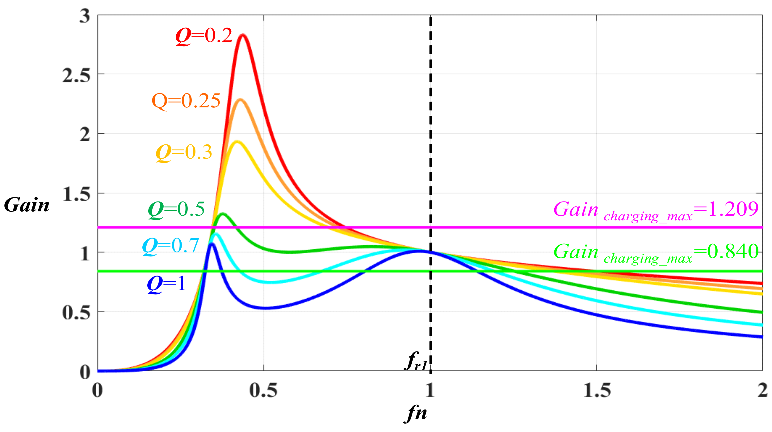
2.2. Transfer Function of the Proposed Bidirectional CL3C Resonant Converter

The equivalent circuit diagram of the proposed resonant converter is shown in Figure 2. The input power is transmitted from left to right. The parameter, vAB, denotes the square-wave voltage after the grid power source is turned on (or off) by using the switch at the primary side, and veq denotes the square-wave voltage obtained after being processed by the resonant circuit and transformer. The parameters jωLr1, 1/jωCr1, jωLm, jωLr2’, and 1/jωCr2’ denote the primary-side resonant inductance Lr1, primary-side resonant capacitance Cr1, magnetizing inductance Lm, secondary-side equivalent resonant inductance Lr2’, and the secondary-side equivalent resonant capacitance Cr2’ in the frequency domain. As expressed in Equation (1), the equivalent impedance Req is the equivalent primary-side AC load impedance derived from the secondary-side battery load impedance.
R e q = N 2 8 π 2 × V B a t   b a n k I B a t   b a n k = 8 N 2 π 2 R B a t   b a n k
Referring to Equation (1), N denotes the turns ratio of the transformer and RBat bank denotes the equivalent load impedance of the battery. The voltage of the first node (vc) is used as the reference voltage, and the voltage divider rule is used to determine the voltage gain equations for describing the relationship between vc and vAB and that between veq and vc Equation (2). Accordingly, the voltage gain function between veq and vAB is determined.
v c = v A B · Z 2 j ω Z 1 j ω v e q = v c · Z 4 j ω Z 3 j ω
In Equation (2), Z1(jω), Z2(jω), Z3(jω), and Z4(jω) denote the equivalent impedances of the corresponding components. The aforementioned parameters can be used to express the transfer function G(jω) of the proposed converter in the charging mode as presented in Equation (3).
G j ω = v e q v A B = v c v A B × v e q v c = Z 2 j ω Z 4 j ω Z 1 j ω Z 3 j ω = j ω L m R e q j ω L m + j ω L r 2 + R e q + 1 j ω C r 2 j ω L r 1 + 1 j ω C r 1 + j ω L m j ω L r 2 + R e q + 1 j ω C r 2
The parameters fr1, fn, Q, k, m, and g are defined in Equation (4) to facilitate the design of the resonance parameters for using simulation software to plot a voltage gain curve based on the transfer function expressed in Equation (3).
f r 1 = 1 2 π L r 1 C r 1 , f n = f s f r 1 , Q = L r 1 C r 1 R o e , k = L m L r 1 , g = C r 2 C r 1 , m = L r 2 L r 1
Equation (4) is substituted into Equation (3) and then simplified. The angular frequency is converted into frequency. Accordingly, the transfer function of the bidirectional CL3C resonant converter in the charging mode can be expressed using Equation (5).
G f n = 1 1 + 1 k 1 k f n 2 2 + Q 2 1 k g f n 3 + f n + m f n k + m f n 1 f n m k f n 1 k g f n 1 g f n 2
The equivalent circuit diagram of the proposed converter in the discharging mode is shown in Figure 3. This equivalent circuit diagram is identical to that of the converter in the charging mode. Therefore, the transfer function is also identical in the charging and discharging modes. In the discharging mode, power is transmitted from right to left.
The transfer function of the bidirectional CL3C resonant converter in the discharging mode is expressed using Equation (6), where f r 2 ,   f n ,   Q ,   k ,   g ,   and   m are simplified parameters that are defined in Equation (7).
G f n = 1 1 + 1 k 1 k ( f n ) 2 2 + Q 2 1 k g ( f n ) 3 + f n + m f n k + m f n 1 f n m k f n 1 k g f n 1 g f n 2
f r 2 = 1 2 π L r 2 C r 2 , f n = f s f r 2 Q = L r 2 C r 2 R o e , k = L m L r 2 , g = 1 g , m = 1 m

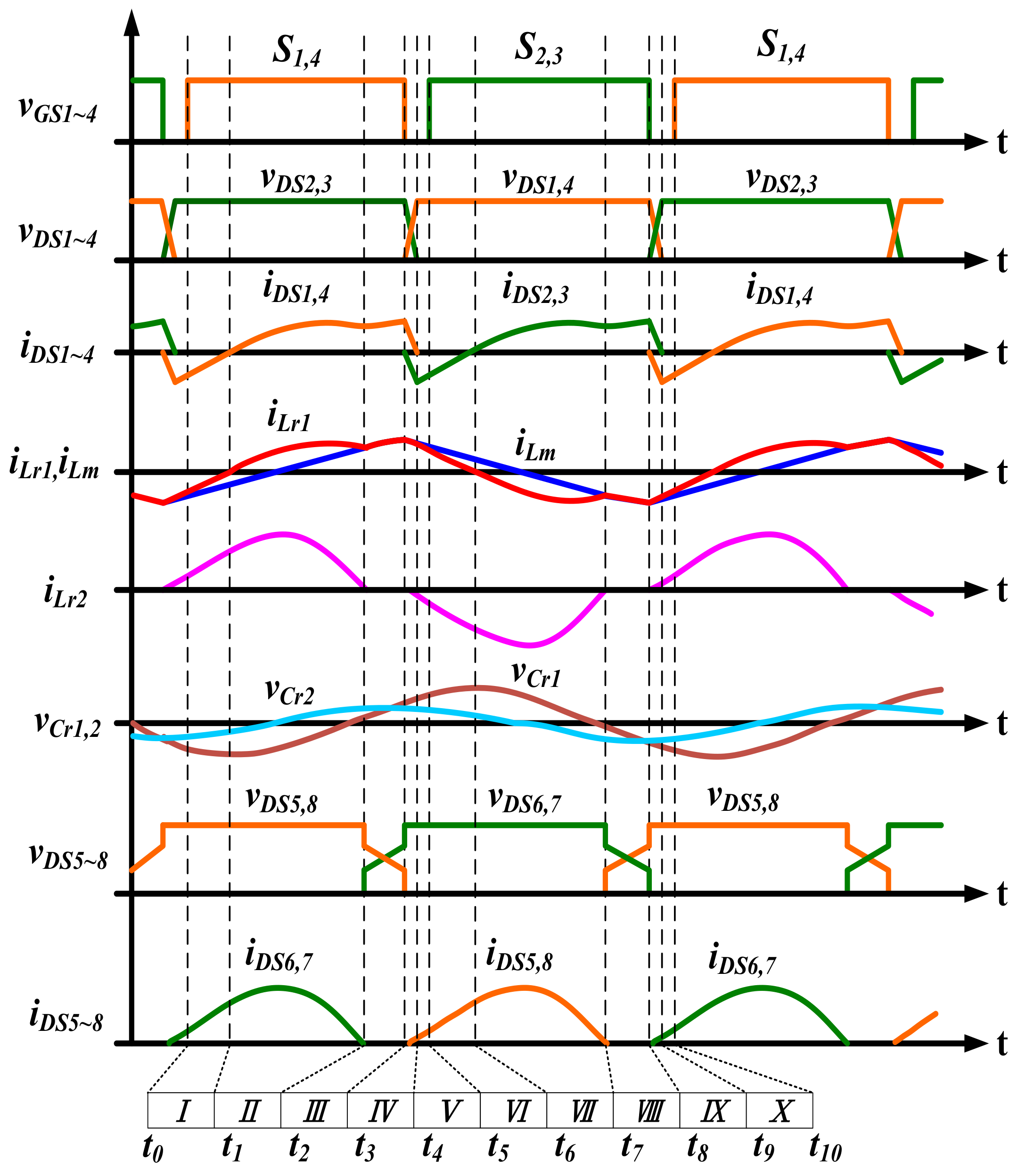
2.3. Circuit Characteristics and Operating Principles of the Proposed Converter

Based on Figure 4, it presents the voltage gain curve of the proposed bidirectional CL3C full-bridge resonant converter in the charging mode. This curve is divided into three regions according to two resonant frequencies, namely, fr1 and fm.
  • For Region 1, the resonant impedance is inductive, and the AC square-wave voltage of the transformer exceeds the resonant current, enabling the power switch to achieve ZVS;
  • For Region 2, the resonant impedance is inductive, and the AC square-wave voltage of the transformer exceeds the resonant current, allowing the power switch to achieve ZVS and the rectifier diode at the rectifier side to achieve ZCS;
  • For Region 3, the resonant impedance is capacitive, and the power switch cannot achieve ZVS. Large variations in the voltage gain were observed in this region. Consequently, operation in this region should be avoided.
The operating circuit diagram of the proposed bidirectional CL3C full-bridge resonant converter is shown in Figure 5. Energy transmitted from the primary-side grid (VDC) passes through the input capacitance CDC, which performs wave filtering and voltage stabilization. Four switches, namely, S1, S2, S3, and S4, were activated, which enables the bidirectional CL3C resonant network (which comprises Cr1, Lr1, Lm, Lr2, and Cr2) and transformer, TR, to transmit the energy from the primary side to the secondary side. Next, the energy is rectified by four power switch body diodes, namely, DS5, DS6, DS7, and DS8, before being transmitted by the output capacitance, CBat bank, to charge the battery. Among the converter control signals, S1 and S4, are identical; S2 and S3 are identical; the left-arm S1 and S2 are complementary; and the right-arm S3 and S4 are complementary. The conduction of each signal does not exceed 50% and includes the duty cycle of dead time. A modulation switch is used to control the energy conversion of the circuit by switching the frequency fs. Figure 6 shows the time series data of the waveform when the power switch is conducted and cutoff during the operation of the proposed converter in Region 2.
The circuit operation is stated in Figure 7. When the proposed converter operates in Region 2, the circuit operating modes in the positive and negative half-cycles are similar. Therefore, this study only examined circuit operations in positive half-cycles. Because the circuit operating principles in the charging and discharging modes were identical, the principles were not discussed further. When the proposed converter operates in Region 2, the primary-side power switch can achieve ZVS, and the secondary side can achieve ZCS. The following assumptions were adopted in this study to expedite the analysis of the circuit operating principles of the proposed converter: for Equation (1), the power switches S1S8 were ideal, and only the body diodes DSB1–DSB8 and parasitic capacitances Coss1–Coss8 were considered; for Equation (2), all resonant components, namely, Cr1, Lr1, Lm, Lr2, and Cr2, were ideal, and no energy was lost during energy storage and discharge; for Equation (3), the output capacitance CBat bank was infinity; for Equation (4), the circuit operated under a steady state.
Mode I (t0–t1):
As shown in Figure 7a, when t = t0, the power switch signals vGS1 and vGS4 were transformed from low-level signals to high-level signals, and the primary-side resonant current, ir1, remained continuous through the equivalent switch body diodes DSB1 and DSB4. When t0 < t < t1, the power switches S1 and S4 were conducted. The power switch currents, iDS1 and iDS4, change from negative to positive, and the power switches, S1 and S4, achieve ZVS. The magnetizing inductance, Lm, is clamped by the output voltage, VBat bank, and secondary-side resonant capacitance, Cr2. Therefore, only the primary-side resonant capacitance, Cr1, and primary-side resonant inductance, Lr1, are in resonance, and the magnetizing inductance current, iLm, increases linearly. When t = t1, the primary-side resonant current, iLr1, becomes 0, and Mode I terminates.
Mode II (t1–t2):
As displayed in Figure 7b, when t = t1, the power switches S1 and S4 are conducted, and the currents iDS1 and iDS4 achieve ZVS. The secondary-side body diodes DSB6 and DSB7 remain conducted under the aforementioned condition. When t1 < t < t2, the DC grid at the input end transmits power to the secondary side through the switching of S1 and S4 and processing by the resonant components Cr1, Lr1, Lr2, and Cr2 and transformer, TR. After the current is rectified by the secondary body diodes DSB6 and DSB7, the power is transmitted to the battery. The magnetizing inductance, Lm, is still clamped by the output voltage, VBat bank, and secondary resonant capacitance voltage, VCr2, and, therefore, does not participate in circuit resonance. Moreover, the magnetizing inductance current, iLm, increases linearly. When t = t2, the primary-side resonant current, iLr1, is equal to the magnetizing inductance current, iLm, and Mode II terminates.
Mode III (t3–t4):
When t = t2, the power switches S1 and S4 remain conducted. The current in the secondary-side body diodes DSB6 and DSB7 decreases to 0 to achieve ZCS. When t2 < t < t3, the converter enters the decoupling region. In this region, the primary-side transformer current ip and secondary-side resonant current ir2 are 0. Therefore, the secondary-side body diodes DSB6 and DSB7 stay cutoff, which fulfills the condition of ZCS. Under the aforementioned conditions, the output energy is only provided by the output capacitance CBat. Thus, the magnetizing inductance, Lm, is not clamped by the output voltage, VBat bank, and secondary resonant capacitance. Consequently, Cr1, Lr1, and Lm participate in circuit resonance. When t = t3, the power switch signals vGS1 and vGS4 are conducted.
Mode IV (t4–t5):
As depicted in Figure 7d, when t = t3, the power switch signals vGS1 and vGS4 are converted from high-level signals to low-level signals. When t3< t < t4, the circuit enters dead time. The primary-side resonant current, iLr1, remains continuous, charges the parasitic capacitances Coss1 and Coss4, and discharges the parasitic capacitances Coss2 and Coss3. The primary-side resonant current, iLr1, is less than the magnetizing inductance current, iLm. Therefore, the magnetizing inductance current, iLm, continues to send energy to the secondary side through the transformer, which causes the body diodes DSB5 and DSB8 to be conducted. When t = t4, the parasitic capacitances Coss1 and Coss4 store energy in the DC grid voltage VDC, the parasitic capacitances Coss2 and Coss3 discharge to zero, and Mode IV terminates.
Mode V (t5–t6):
As shown in Figure 7e, when t = t4, the parasitic capacitances Coss1 and Coss4 store energy in the DC grid voltage VDC, and the parasitic capacitances Coss2 and Coss3 discharge to zero. When t3 < t < t4, the flow of the primary-side resonant current, iLr1, is maintained through the body diodes DSB2 and DSB3. At this time, the primary-side resonant current, iLr1, remains smaller than the magnetizing inductance current, iLm. Therefore, the primary-side transformer current, ip, is still transmitted to the secondary side through the transformer, enabling the body diodes DSB5 and DSB8 to stay conducted. When t = t4, the power switch signals vGS2 and vGS3 are converted from low-level signals to high-level signals. Moreover, the power switches S2 and S3 are conducted and achieve ZVS, and Mode V terminates. Accordingly, the operation in the positive half-cycle ends. Because the operations in the positive and negative half-cycles are similar, only the circuit operation in the positive half-cycle is discussed in this paper.

3. Circuit Design

3.1. Design Focuses

3.1.1. Ability to Adjust the Voltage According to the Battery Conditions

When the proposed converter operates in the charging mode, its circuit should be able to achieve a wide output voltage range by increasing the output voltage from the minimum level to the maximum level according to the battery voltage. Similarly, when operating in the discharging mode, the circuit should be able to achieve a wide input voltage range by reducing the input voltage from the maximum level to the minimum level according to the battery voltage.
Because a converter can adjust the output voltage by using its resonant tank and transformer, the turns ratio N must be defined to determine the maximum and minimum gains required by the transformer and expedite the subsequent design process. The turns ratio is expressed in Equation (8).
N = N P N S = V D C V B a t _ n o m
After the turns, ratio N is determined, the maximum voltage, VBat_max, and minimum voltage, VBat_min of the battery are substituted into Equations (9) and (10), respectively, to calculate the maximum and minimum gains required by the transformer, respectively. Accordingly, the maximum and minimum gains required by the resonant tanks in the charging mode can be determined to verify the ability of the converter to achieve a wide output range.
G a i n c h a r g i n g _ m a x = N × V B a t _ m a x V D C
G a i n c h a r g i n g _ m i n = N × V B a t _ m i n V D C
The maximum and minimum gains required by the resonant tank in the discharging mode are stated in Equations (9) and (10) to express the maximum and minimum gains required by the resonant tank in the discharging mode, respectively. The solutions calculated using these equations are used to verify the ability of the proposed converter to achieve a wide input range.

3.1.2. Ability to Achieve a High Charging Efficiency

Converters should operate in Region 2 for efficiently achieving constant current (CC)–constant voltage (CV) charging, because supply-side ZVS and rectifier-side ZCS can be achieved in this region, which considerably reduces the power loss caused by switching. For a converter to operate in Region 2, the voltage gain must be greater than 1. Therefore, the input and output voltages must be matched with the turn ratio of the transformer.
The following two figures present the CC–CV curves for turns ratio (N) of 1.08 and 1.2, respectively. When the converter’s charging voltage was higher than 369.6 V and N was 1.08, the resonant tank operated in Region 2 while stepping up the voltage (Figure 8). When the transformer’s charging voltage was higher than 333.3 V and N was 1.2, the resonant tank operated in Region 2 while stepping up the voltage (Figure 9). The aforementioned results verify that adjusting the turns ratio N can increase the duration for which the converter operates in Region 2, which increases the overall charging efficiency.

3.2. Circuit Design Procedure

The voltage gain curve displayed in Figure 4 and the CC–CV curves displayed in Figure 8 and Figure 9 were referenced to design a bidirectional resonant charging circuit with adjustable output power. The design procedure is described as follows:
Step 1: Equation (8) is used to calculate the transformer turns ratio;
Step 2: Equations (9)–(12) are used to determine the maximum and minimum gains in the charging and discharging modes;
Step 3: The turns ratio of the transformer is adjusted to increase the duration for which the converter operates in Region 2, which would increase the overall charging efficiency;
Step 4: A set of values is selected for Q, k, m, and g by analyzing voltage gain curves. The selected parameters are used to plot curves in a summation software program, and the plotted curves are analyzed. Figure 10 presents the voltage gain curves for different Q values when k = 4. The maximum and minimum gains required in the charging mode are also indicated in this figure. The aforementioned curves facilitate a preliminary analysis of whether the selected parameters fulfill the maximum and minimum gain requirements of the circuit. On the basis of the preliminary analysis, a Q value of 0.27 is selected for designing the circuit. The remaining parameters (i.e., k, m, and g) are selected in a similar manner;
Step 5: After determining appropriate values for Q, k, m, and g, Equation (4) is used to calculate the parameters of the resonant components.
Step 6: The parameters of the resonant components determined in the charging mode are used to derive the Q ,   k ,   m ,   and   g values required for the discharging mode. Voltage gain curves are plotted according to the derived parameter values, and the maximum and minimum voltage gains required for the discharging mode are indicated in the figure displaying these curves. The aforementioned curves and information can be used to conduct a preliminary analysis of whether the derived parameters fulfill the maximum and minimum gains required by the circuit;
Step 7: Step 3 is repeated if the maximum and minimum gain requirements for the charging and discharging modes are not met. The resonance parameters are readjusted until these requirements are met. Finally, the parameters that fulfill the voltage gain requirements are used to plot voltage gain curves. The maximum and minimum gains required for the charging and discharging modes are presented in the figure displaying these curves as shown in Figure 11. The maximum and minimum operating frequencies of the converter in the charging and discharging modes can then be determined from this figure.

4. Digital Feedback Control

Today, common charging methods include CC, CV, CC–CV, and pulse charging. Among these methods, CC–CV charging is the most widely used charging method because it resolves the problems associated with charging currents with excessively large voltages and overcharging currents. CC–CV charging enables fast battery charging and prevents battery overcharging.

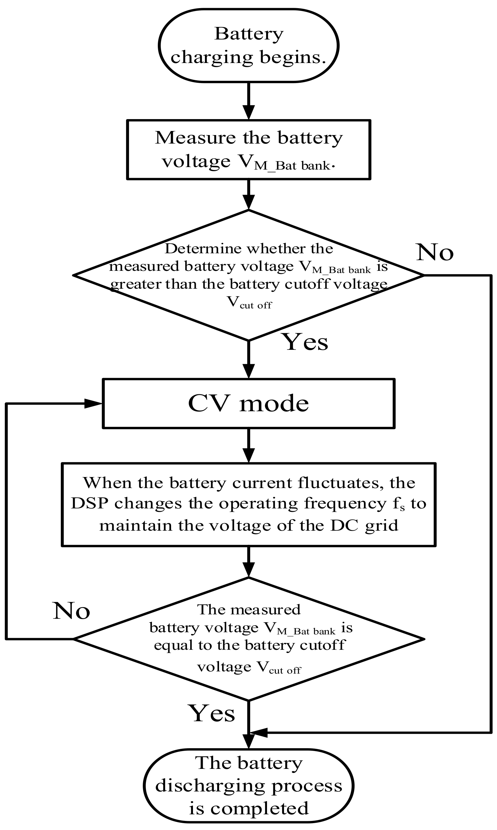
4.1. Control of the Charging Mode

The control framework of the proposed bidirectional CL3C full-bridge resonant converter for the charging mode is shown in Figure 12. When the converter is in the CC mode, the current sensor determines the battery current IBat bank, reduces it, and subtracts the battery current signal from the reference current signal to acquire an error signal value. A proportional–integral controller is then used to compensate for the error before the battery current signal is sent to the computation chip to achieve CC charging. When the converter is in the CV mode, the voltage sensor determines the battery voltage VBat bank, reduces it, and subtracts the battery voltage signal from the reference signal to acquire an error signal value. The proportional–integral controller is then used to compensate for the error before the battery voltage signal is sent to the computation chip to achieve CV charging.
The flowchart of the proposed CC–CV charging method is shown in Figure 13. When a battery begins to charge, a digital signal processor (DSP) detects the battery voltage, VBat bank, and then determines the battery cutoff voltage, Vcut off. Next, the DSP determines whether the battery voltage is higher than the preset CC–CV voltage, VCC–CV. If the battery voltage is smaller than the preset CC–CV voltage, the DSP signals the converter to operate in the CC mode. When the battery is charged by a CC, the DSP continues to detect the battery voltage. If the battery voltage is higher than the present CC–CV voltage, VCC–CV, the DSP signals the converter to operate in the CV mode. When the battery is charged by a CV, the DSP continues to detect the battery current, IBat bank. The charging process is completed when the battery current is less than or equal to the preset battery cutoff current Icut off. Under this condition, the DSP sends a termination signal to the power switch to turn off the converter.

4.2. Control of the Discharging Mode

The control framework of the proposed bidirectional CL3C full-bridge resonant converter for the discharging mode is shown in Figure 14. A stable DC grid voltage is used in this mode, and the converter outputs a CV. Therefore, the voltage sensor determines the grid voltage VDC, reduces it, and subtracts the grid voltage signal from the reference signal to acquire an error signal value. A proportional–integral controller is used to compensate for the error before the grid voltage signal is sent to the computation chip to achieve CV discharging from the converter to the grid.
The flowchart of the proposed battery energy storage system discharging method is shown in Figure 15. When the battery begins to discharge, the DSP detects the battery voltage VBat bank and then determines whether the battery voltage is greater than the present battery cutoff voltage. If the battery voltage is smaller than the cutoff voltage, the battery is completely drained, and the DSP immediately signals the converter to stop operating. If the battery voltage is greater than the cutoff voltage, the DSP signals the converter to operate in the CV mode. During CV discharging from the battery to the grid, the DSP continuously monitors the battery voltage VBat bank. If the battery voltage is equal to the battery cutoff voltage, Vcut off, the discharging process is terminated. Under this condition, the DSP stops signaling the power switch, which causes the converter to stop operating and prevents damage to the battery.

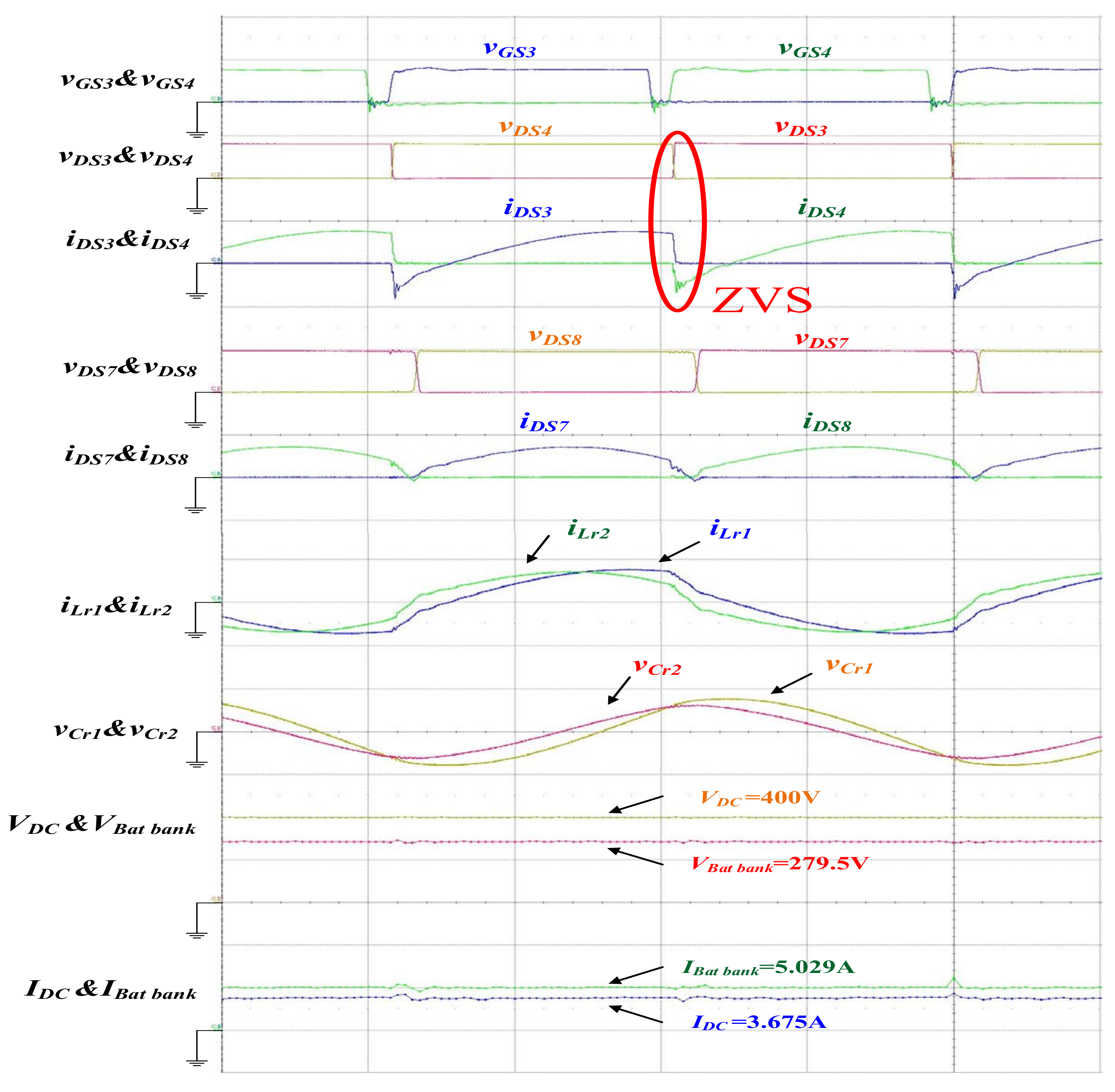
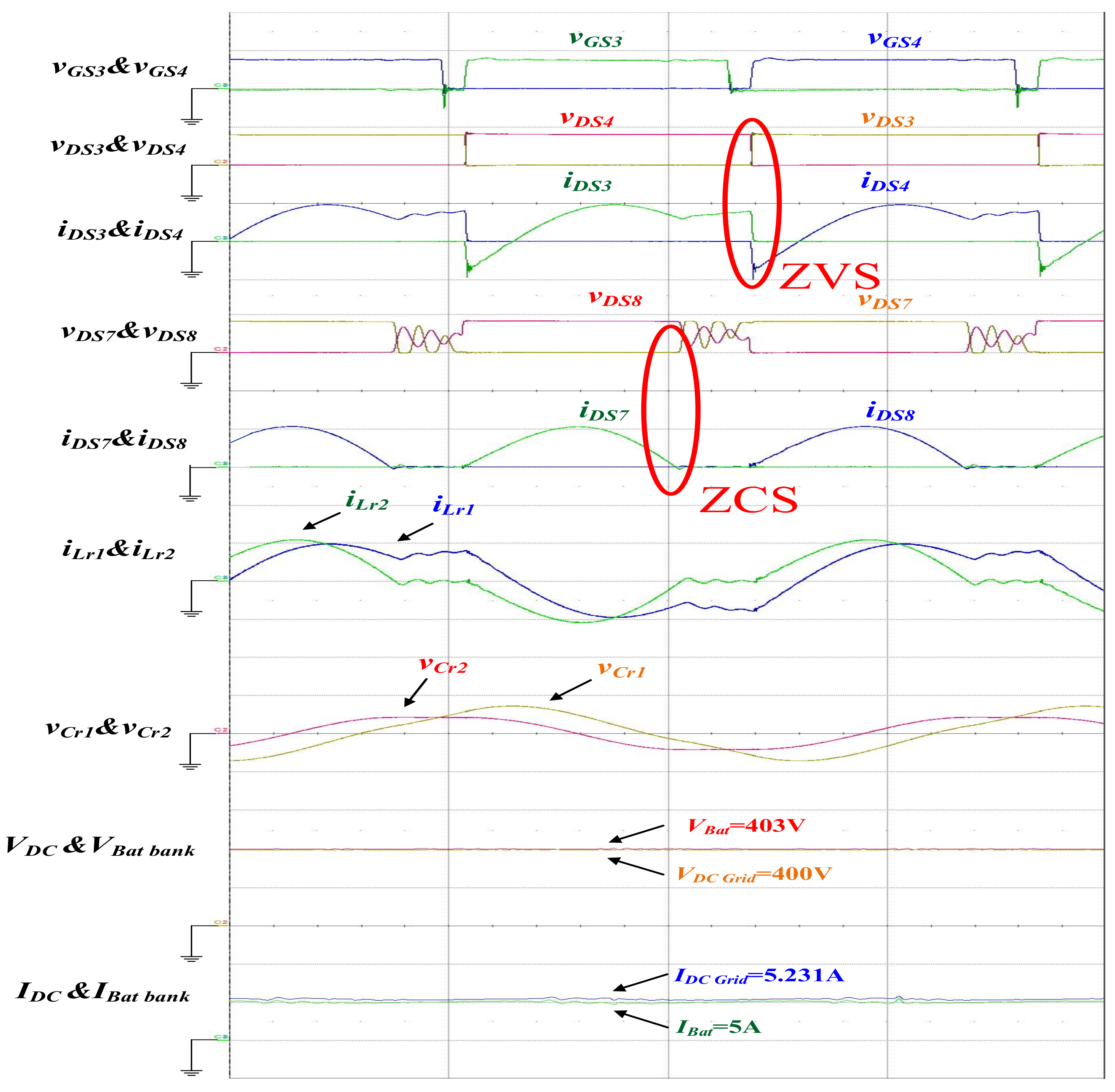
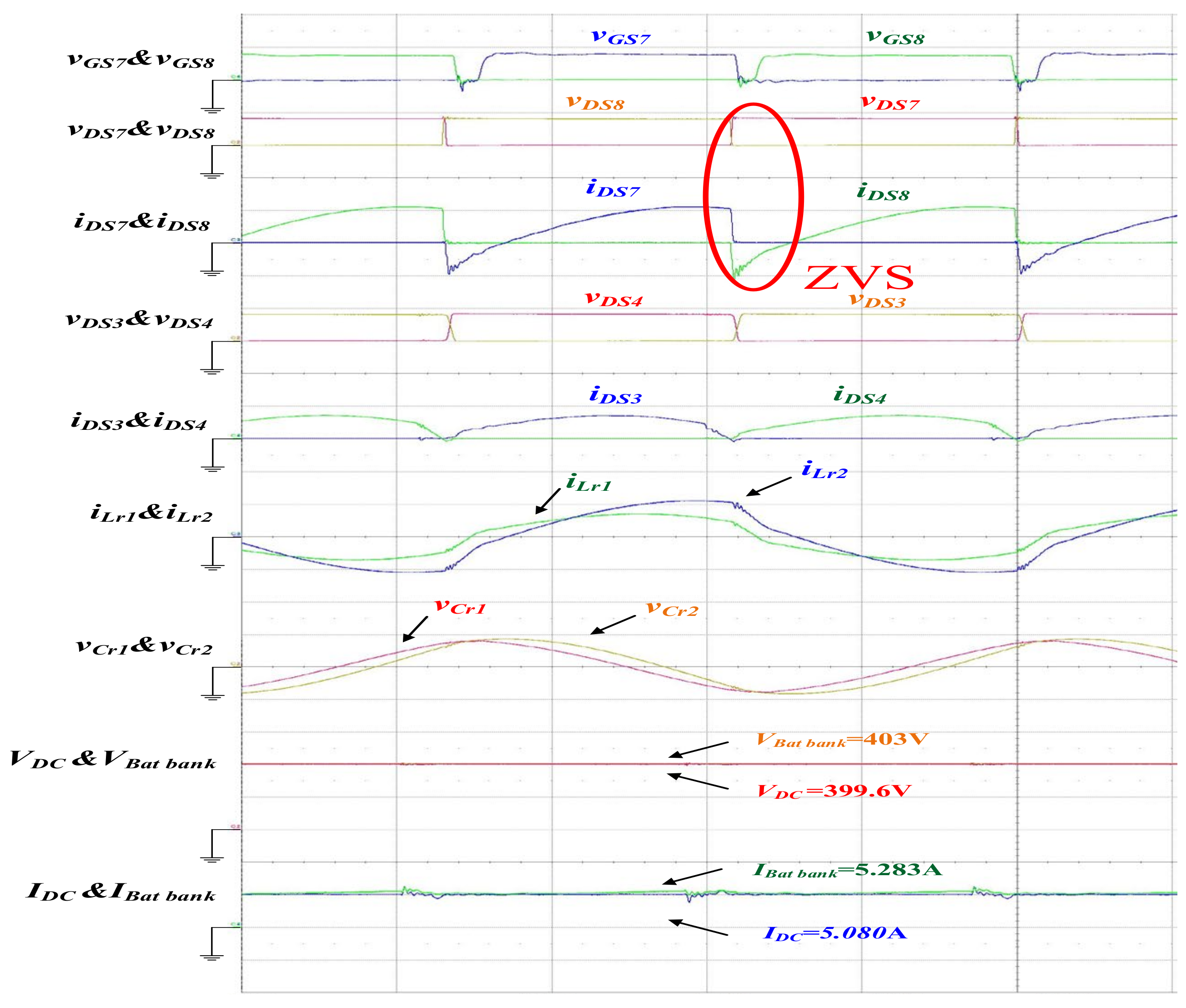
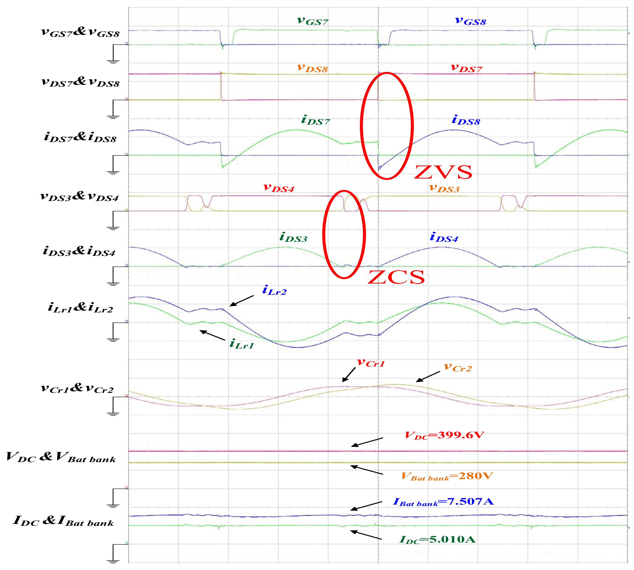
5. Experimental Results

In this study, a 2 kW CL3C bidirectional full-bridge resonant converter was fabricated, and its ability to control bidirectional power transmission between an energy storage system and a DC grid was verified. Table 1 lists the circuit specifications of the aforementioned converter. Table 2 presents the parameter configuration and components used in the fabricated converter. The resonant parameters were as follows: k = 4, Q = 0.27, g = 1, and m = 1. However, the actual parameter configuration of the components differed marginally from the designed parameter values. Nevertheless, these minor differences did not affect the circuit operation.

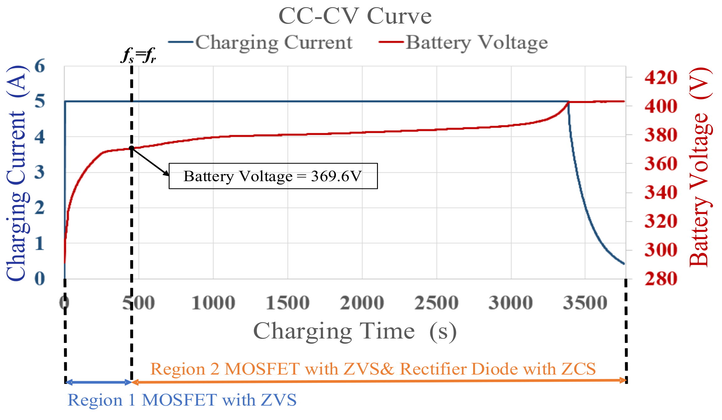
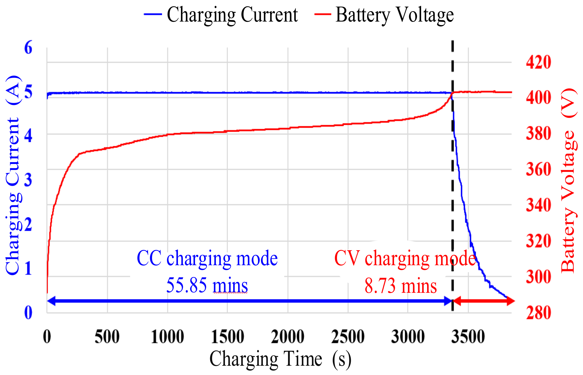
5.1. Key Waveforms, CC–CV Curves, and Charging Efficiency of the Fabricated Converter in the Charging Mode

Key waveforms of the vGS3,4, vDS3,4, iDS3,4, iLr1,2, vcr1,2, vDS7,8, iDS7,8, VDC, VBat bank, and IBat bank are shown in Figure 16 and Figure 17. IDC waveforms were observed when the fabricated converter was operated at full load; the input voltage, VDC, was 400 V; the output voltages, VBat bank, were 280 and 403 V. The results reveal that before the power switches S3,4 were conducted, a reverse current iDS3,4 passed through. This current helped the power switch to discharge the energy stored in the parasitic capacitance, allowing the switch voltage stress vDS3,4 to decrease rapidly to 0 V; thus, ZVS was achieved.
As shown In Figure 16, the current iDS7,8 did not reduce to 0 A before the rectifier diode was cutoff. This phenomenon impeded the ZCS function of the rectifier-side diode, which resulted in an increase in the energy loss and a decrease in the circuit efficiency. Figure 17 indicates that the current iDS7,8 reduced to 0 A before the rectifier diode was cutoff. This condition fulfills the requirement for ZCS, which was achieved as soon as the rectifier diode was cutoff.
Figure 18 displays the CC–CV charging curve obtained when the fabricated converter was used to charge a 1 C and 5 Ah battery. The charging process ended when the charging current was lower than the recommended current of 0.25A. The goal of conducting the aforementioned charging process was to verify that the fabricated converter could be used to perform CC–CV charging.
Figure 19 depicts the charging efficiency curve of the fabricated converter. When the converter operated in the CV mode and the output power was 1600 W, the maximum charging efficiency reached 96.64%.

5.2. Key Waveforms, CC–CV Curves, and Charging Efficiency of the Fabricated Converter in the Discharging Mode

Key waveforms are shown in Figure 20 and Figure 21. IDC waveforms were observed when the fabricated converter was operated at full load, and the input voltages, VBat bank, were 280 and 403 V, and the output voltage, VDC, was 400 V. The results reveal that before the power switches, S7,8, was conducted, a reverse current iDS7,8 passed through. This current helped the power switch to discharge the energy stored in the parasitic capacitance, allowing the switch voltage stress vDS7,8 to decrease rapidly to 0 V; thus, ZVS was achieved.
As shown in Figure 20, the current iDS3,4 did not reduce to 0 A before the rectifier diode was cutoff. This phenomenon impedes the ZCS function of the rectifier-side diode, which results in an increase in the energy loss and a decrease in the circuit efficiency. Figure 21 indicates that the current iDS3,4 was reduced to 0 A before the rectifier diode was cutoff. This condition fulfilled the requirement for ZCS, which was achieved as soon as the rectifier diode was cutoff. The parasitic capacitance and secondary resonant inductance caused the resonance of the rectifier diode voltage stress vDS3,4.
Figure 22 presents the discharging curve obtained when the fabricated converter was used to discharge power to a DC grid at a constant power of 2 kW. The discharging process ends when the battery voltage is equal to the recommended cutoff voltage of 280 V. The aim of conducting this process was to verify that the proposed converter can be used to charge batteries as well as discharge power from batteries to DC grids.
The charging efficiency curve of the fabricated converter is shown in Figure 23. When the converter operated in the CV mode and the input power was 340 W, the maximum discharging efficiency reached 95.8%.

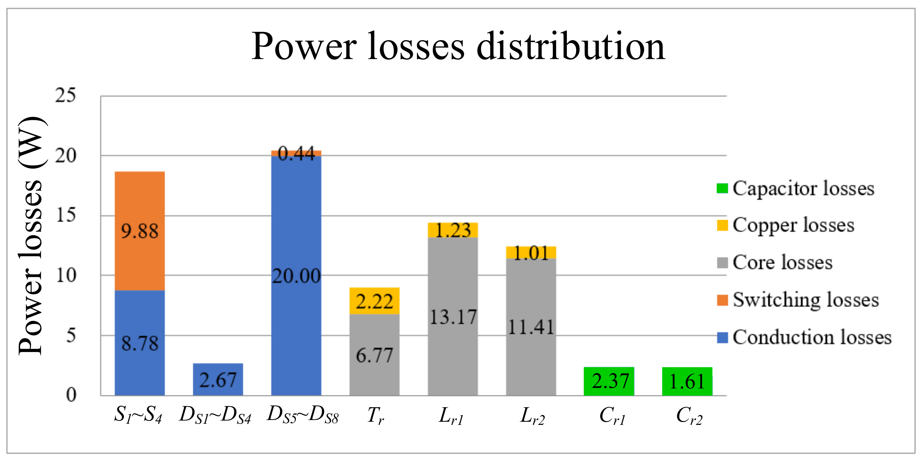
5.3. Analysis of the Voltage–Current Stresses for Power Switches and the Power Losses Distribution of the Proposed Converter

Table 3 and Table 4 show the voltage stress and current stress of the power switches and diodes for the primary and secondary sides. The maximum voltage and current stresses were analyzed and measured. All the analyzed voltage and current stress equations are referred from [15]. The maximum stresses came from the input side and the output side. The voltage stress was caused by the input voltage source (VDC was 400 V). In addition, the current stress was influenced by the current from the battery packs. In Figure 24, the power losses distribution was calculated and summarized. Moreover, the prototype of the proposed converter is also shown in Figure 25.
The power losses distribution is shown in Figure 24. All the power losses of the components were measured under the full load condition, where the output voltage and current were 403 V and 5 A. The maximum voltage and current stresses were analyzed and measured. The maximum stresses came from the input side and the output side. The voltage stress was caused by the input voltage source (VDC was 400 V). In addition, the current stress was influenced by the current from the battery packs.
The power losses distribution was also analyzed and displayed in percentage. For the power switches S1~S4, the conduction losses were 0.44%, and the switching losses was 0.50%. For the body diodes DS1~DS4, the conduction losses was 0.13%. For the rectifier diodes DS5~DS8, the conduction losses were 1%, and the witching losses were 0.02%. The total losses of the main transformer Tr was 0.45%. The core losses of Lr1 was 0.66%, and the copper losses were 0.06%. The core losses of Lr2 was 0.57%, and the copper losses were 0.05%. For the resonant capacitor Cr1, the capacitor losses were 0.12%, and capacitor losses of Cr2 were 0.08%. To sum up, for the power losses of these components, they took 4.08% of the power losses of the entire input power.

6. Conclusions

In this study, a bidirectional CL3C full-bridge resonant converter for DC grids was designed and fabricated. One resonant inductance and one resonant capacitance were installed at the secondary side of a conventional LLC resonant converter to form the framework of the designed converter. Moreover, power switches were installed at the primary and secondary sides to achieve bidirectional energy transmission. Resonance technology was employed to achieve supply-side ZVS and rectifier-side ZCS in the forward and reverse modes of operation, which increased the overall circuit efficiency. Finally, digital control technology was used to achieve CC–CV charging of the battery and to discharge energy to DC grids at a constant power of 2 kW. When the input voltage was 400 V, output voltage was 280 or 403 V, the maximum output power was 2000 W, and the maximum efficiency of the fabricated converter reached 96.64% in the charging mode. When the input voltage was 280 or 403 V, output voltage was 400 V, maximum output power was 2000 W, and the maximum efficiency of the fabricated converter reached 95.79% in the discharging mode. When the battery voltage was 280–380 V, the energy conversion efficiency of the converter exceeded 95%. The proposed converter can be used for off-board vehicle chargers. This application is also suitable for secluded and power shortage regions to achieve the concept of V2V (vehicle to vehicle). Moreover, each EV can be treated as an independent portable power source. The residual energy of EV can be supplied to the grid for achieving the purpose power regulation, G2V, and V2G for future goals.

Author Contributions

Conceptualization, Y.-N.C. and Z.-X.P.; methodology, Y.-N.C.; software, Y.-H.Y.; writing—original draft preparation, Y.-H.Y.; writing—review and editing, Y.-H.Y. and Y.-N.C. All authors have read and agreed to the published version of the manuscript.

Funding

This research received no external funding.

Conflicts of Interest

The authors declare no conflict of interest.

References

  1. Habib, S.; Khan, M.M.; Abbas, F.; Ali, A.; Faiz, M.T.; Ehsan, F.; Tang, H. Contemporary trends in power electronics converters for charging solutions of electric vehicles. CSEE J. Power Energy Syst. 2020, 6, 911–929. [Google Scholar]
  2. Ryu, M.; Jung, D.; Baek, J.; Kim, H. An optimized design of bi-directional dual active bridge converter for low voltage battery charger. J. Power Electron. 2014, 14, 177–183. [Google Scholar] [CrossRef]
  3. Zhao, B.; Song, Q.; Liu, W.; Sun, Y. Overview of Dual-Active-Bridge Isolated Bidirectional DC–DC Converter for High-Frequency-Link Power-Conversion System. IEEE Trans. Power Electron. 2013, 29, 4091–4106. [Google Scholar] [CrossRef]
  4. Bai, H.; Mi, C. Eliminate Reactive Power and Increase System Efficiency of Isolated Bidirectional Dual-Active-Bridge DC-DC Converters Using Novel DualPhase-Shift Control. IEEE Trans. Power Electron. 2008, 23, 2905–2914. [Google Scholar] [CrossRef]
  5. Zhao, B.; Song, Q.; Liu, W. Efficiency Characterization and Optimization of Isolated Bidirectional DC–DC Converter Based on Dual-Phase-Shift Control for DC Distribution Application. IEEE Trans. Power Electron. 2012, 28, 1711–1727. [Google Scholar] [CrossRef]
  6. Li, H.; Zhang, Z.; Wang, S.; Tang, J.; Ren, X.; Chen, Q. A 300-kHz 6.6-kW SiC Bidirectional LLC Onboard Charger. IEEE Trans. Ind. Electron. 2020, 67, 1435–1445. [Google Scholar] [CrossRef]
  7. Awasthi, A.; Bagawade, S.; Kumar, A.; Jain, P. An Exact Time Domain Analysis of DCM Boost Mode LLC Resonant Con-verter for PV applications. In Proceedings of the IECON 2018—44th Annual Conference of the IEEE Industrial Electronics Society, Busan, Korea, 21–23 October 2018; pp. 1005–1010. [Google Scholar]
  8. Liu, Y.; Du, G.; Wang, X.; Lei, Y. Analysis and Design of High-Efficiency Bidirectional GaN-Based CLLC Resonant Con-verter. Energies 2019, 12, 3859. [Google Scholar] [CrossRef] [Green Version]
  9. Chen, W.; Wang, S.; Hong, X.; Lu, Z.; Ye, S. Fully soft-switched bidirectional resonant dc-dc converter with a new CLLC tank. In Proceedings of the 2010 Twenty-Fifth Annual IEEE Applied Power Electronics Conference and Exposition (APEC), Palm Springs, CA, USA, 21–25 February 2010; pp. 1238–1242. [Google Scholar]
  10. Liu, C.; Sen, B.; Wang, J.; Gould, C.; Colombage, K. A CLLC Resonant Converter Based Bidirectional EV Charger with Maximum Efficiency Tracking. In Proceedings of the 8th IET International Conference on Power Electronics, Machines and Drives (PEMD 2016), Glasgow, UK, 19–21 April 2016. [Google Scholar] [CrossRef]
  11. Chang, H.-T.; Liang, T.-J.; Yang, W.-C. Design and Implementation of Bidirectional DC-DC CLLLC Resonant Converter. In Proceedings of the 2018 IEEE Energy Conversion Congress and Exposition (ECCE), Portland, OR, USA, 23–27 September 2018; pp. 2712–2719. [Google Scholar] [CrossRef]
  12. Zahid, Z.U.; Dalala, Z.M.; Chen, R.; Chen, B.; Lai, J. Design of Bidirectional DC–DC Resonant Converter for Vehicle-to-Grid (V2G) Applications. IEEE Trans. Transp. Electrif. 2015, 1, 232–244. [Google Scholar] [CrossRef]
  13. Song, J.; Yang, D.; Zhang, C.; Duan, B. Hybrid Control Method for CLLLC Resonant Converter with Low Output Voltage Ripple. IFAC-PapersOnLine 2018, 51, 31. [Google Scholar] [CrossRef]
  14. Huang, H. Designing an LLC Resonant Half-Bridge Power Converter; Texas Instruments: Dallas, TX, USA, 2010. [Google Scholar]
  15. Rafiq, U.; Murtaza, A.; Sher, H.; Gandini, D. Design and Analysis of a Novel High-Gain DC-DC Boost Converter with Low Component Count. Electronics 2021, 10, 1761. [Google Scholar] [CrossRef]
Figure 1. Circuit diagram of the proposed bidirectional CL3C full-bridge resonant converter.
Energies 15 00412 g001
Figure 2. Equivalent circuit diagram of the proposed bidirectional CL3C resonant converter in the charging mode.
Energies 15 00412 g002
Figure 3. Equivalent circuit diagram of the proposed bidirectional CL3C resonant converter in the discharging mode.
Energies 15 00412 g003
Figure 4. Voltage gain curve of the proposed bidirectional CL3C resonant converter in the charging mode.
Energies 15 00412 g004
Figure 5. Operating circuit diagram of the proposed bidirectional CL3C full-bridge resonant.
Energies 15 00412 g005
Figure 6. Time series data of the proposed converter when it operates in Region 2.
Energies 15 00412 g006
Figure 7. Circuit diagrams of the proposed bidirectional CL3C full-bridge resonant converter for operation in the charging mode: (a) Mode I, (b) Mode II, (c) Mode III, (d) Mode IV, and (e) Mode V.
Energies 15 00412 g007aEnergies 15 00412 g007b
Figure 8. CC–CV curve when N = 1.08.
Energies 15 00412 g008
Figure 9. CC–CV curve when N = 1.2.
Energies 15 00412 g009
Figure 10. Voltage gain curves for different Q values.
Energies 15 00412 g010
Figure 11. Voltage gain curves under the charging and discharging modes.
Energies 15 00412 g011
Figure 12. Control framework of the proposed bidirectional CL3C full-bridge resonant converter for the charging mode.
Energies 15 00412 g012
Figure 13. Flowchart of the proposed CC–CV battery energy storage system charging method.
Energies 15 00412 g013
Figure 14. Control framework of the proposed CL3C full-bridge resonant converter for the discharging mode.
Energies 15 00412 g014
Figure 15. Flowchart of the proposed method for battery energy storage system discharging to a DC grid.
Energies 15 00412 g015
Figure 16. Waveforms obtained when the output battery voltage, VBat bank, was 280 V and the fabricated converter was operated at full load (vGS3&4: 20 V/div, vCr1&2, and VDC; VBat bank: 200 V/div; vDS7&8: 300 V/div; vDS3&4: 500 V/div; iDS3&4, iLr1&2, iDS7&8: 10 A/div; IBat bank, IDC: 5 A/div).
Energies 15 00412 g016
Figure 17. Waveforms obtained when the output battery voltage, VBat bank, was 403 V and the fabricated converter was operated at full load (vGS3&4: 20 V/div; vDS3&4, VDC, VBat bank: 200 V/div; vCr1&2, vDS7&8: 500 V/div; iDS3&4, iLr1&2, iDS7&8: 10 A/div; IBat bank, IDC: 5 A/div).
Energies 15 00412 g017
Figure 18. CC–CV charging curve of the fabricated converter.
Energies 15 00412 g018
Figure 19. CC–CV charging efficiency curve of the fabricated converter.
Energies 15 00412 g019
Figure 20. Waveforms obtained when the input battery voltage, VBat bank, was 403 V and the fabricated converter was operated at full load (vGS7&8: 20 V/div; vCr1&2, VDC, VBat bank: 200 V/div; vDS7&, vDS3&4: 500 V/div; iDS7&8, iLr1&2, iDS3&4: 10 A/div; IBat bank, IDC: 5 A/div).
Energies 15 00412 g020
Figure 21. Waveforms obtained when the input battery voltage, VBat bank, was 280 V and the fabricated converter was operated at full load (vGS7&8: 20 V/div; vDS7&8, VDC, VBat bank: 200 V/div; vCr1&2, vDS3&4: 500 V/div; iDS7&8, iLr1&2, iDS3&4: 10 A/div; IBat bank, IDC: 5 A/div).
Energies 15 00412 g021
Figure 22. Constant power discharging curve of the fabricated converter.
Energies 15 00412 g022
Figure 23. Constant power discharging efficiency curve of the fabricated converter.
Energies 15 00412 g023
Figure 24. Power losses distribution in the proposed converter operated in the full load condition.
Energies 15 00412 g024
Figure 25. The prototype of the proposed converter.
Energies 15 00412 g025
Table 1. Electrical specifications of the fabricated converter.
ParameterValue
DC grid voltage, VDC400 V
Battery voltage, VBat bank280~403 V
Maximum conversion power. P2000 W
Maximum conversion current, I5 A
Resonance frequency, fr100 kHz
Table 2. Parameter configuration and components used in the fabricated convertor.
Component ParameterValue
Turns ratio of the transformer, N1.21
Primary-side resonant capacitance, Cr160 nF
Secondary-side resonant capacitance, Cr281 nF
Magnetizing inductance, Lm166.5 μH
Primary-side resonant inductance, Lr138.55 μH
Secondary-side resonant inductance, Lr228.55 μH
DC grid capacitance, CDC540 μF
Battery capacitance, CBat bank540 μF
Power switches, S1–S8UJ3C065080K3S
DSPTMS320F28335
Table 3. Voltage stress of the power switches and diodes for the primary and secondary sides.
f (Hz)S1~S4 (V)DS1~DS4 (V)S5~S8 (V)DS5~DS8 (V)
70k400400465465
80k400400398398
90k400400361361
100k400400337337
110k400400320320
120k400400300300
130k400400277277
140k400400251251
150k400400225225
Table 4. Current stress of the power switches and diodes for the primary and secondary sides.
f (Hz)S1~S4 (A)DS1~DS4 (A)S5~S8 (A)DS5~DS8 (A)
RmsPeakRmsPeakRmsPeakRmsPeak
70k5.410.51.619.2004.811.6
80k4.69.31.236.9004.510.0
90k4.28.51.125.9004.29.1
100k4.08.11.085.3004.08.3
110k3.97.80.955.5003.87.7
120k3.87.91.106.4003.87.4
130k3.88.11.317.4003.97.4
140k3.78.41.528.0003.97.4
150k3.68.71.728.2003.97.7
Publisher’s Note: MDPI stays neutral with regard to jurisdictional claims in published maps and institutional affiliations.

