Article

An Improved Down-Scale Evaluation System for Capacitors Utilized in High-Power Three-Phase Inverters under Balanced and Unbalanced Load Conditions

Department of Electrical Engineering, National Central University, Taoyuan City 320, Taiwan
*
Author to whom correspondence should be addressed.
Energies 2022, 15(19), 6937; https://doi.org/10.3390/en15196937
Submission received: 1 August 2022 / Revised: 6 September 2022 / Accepted: 19 September 2022 / Published: 22 September 2022

Abstract

:
The DC-link capacitors in an electronic power system are the main constraint of the power density and lifespan of the power converters. Evaluating the load life of capacitors working in severely adverse circumstances plays an important role in the design stages of the next-generation power converters. In this article, an improved evaluation system for the capacitors utilized in high-power three-phase voltage source inverters is proposed. The purpose of this article is to reproduce the same encountered stresses when a DC-link capacitor is used in a high-power inverter with pulse-width modulation. Hence, an improved down-scale evaluation system for the DC-link capacitors used in high-power three-phase inverter systems under balanced and unbalanced load conditions is proposed. Moreover, AC and DC analyses in the proposed evaluation system are conducted. The equivalent circuit and transfer functions are derived to verify the proposed evaluation system. Finally, a prototype system is constructed to facilitate the theoretical results as the verification.

1. Introduction

Due to the development of renewable energy, more and more high-power and high-density inverters are being manufactured for PVs, wind power systems and fuel cells, etc. Therefore, the system testing for high-power and high-density inverters becomes very important, especially in the limited power-rating testing field. Although the International Electrotechnical Commission (IEC) has established some testing standards for distributed systems, such as IEC 60364-7-712:2017 [1] and IEC 61000-3-3:2013+AMD1:2017+AMD2:2021 [2], and IEC/TS 61000-3-4 [3], etc., there still exist some issues in the testing field. If the power capacity of the testing field is smaller than that of the equipment under test (EUT), the high-power EUT cannot be tested under a full-scale power rating. Hence, some evaluation circuits and/or evaluation methods [4,5,6,7,8,9,10,11] for high-power converters were proposed. They are intended to reproduce the same encountered stresses for any components of high-power converters. However, the main constraint of the power density and lifespan of power converters is the DC-link capacitor. Generally, the life cycle of capacitors is usually shorter than that of the magnetic components and semiconductor devices. Therefore, evaluating the load life of capacitors working in severely adverse circumstances plays an important role in the design stages of the next-generation power converters, especially in the evaluation of the capacitors in terms of the power loss, ageing, and failure rate.
Nevertheless, in the past decades, only a single sinusoidal current was used to evaluate the quality of capacitors, such as 120 Hz and 1 kHz [4]. In addition, a ripple current tester and a DC bias are used to test the capacitors [5,12]. However, the current that flows from the converter to the capacitors (EUT) contains multiple frequency components. Although the frequency components can be correctly analyzed, it should be noted that the power loss of capacitors with respect to frequencies is a non-linear characteristic [6,7,8,13]. In order to understand the aging characteristics, it is necessary to monitor the aging parameters of the capacitor under test in the actual scenario. Generally, there are three kinds of estimation methods, i.e., offline, quasi-online, and online methods. A quasi-online method was proposed in [14], where a specific switch is used to stop the inverter and an LC resonant network is introduced. The DC-link capacitor value is estimated by analyzing the collected current data. However, this method requires additional control design, which limits its application. In [9], a variable electrical network monitoring method was proposed. During the inverter shutdown period, the capacitors are discharged through the controlled variable electrical network, and the capacitance value and equivalent series resistance (ESR) are estimated, based on the observed discharge curve. Considering that the accelerated aging test is a long process, frequent shutdowns of the system will increase the burden of the system, and online estimation can avoid this shortcoming. In [
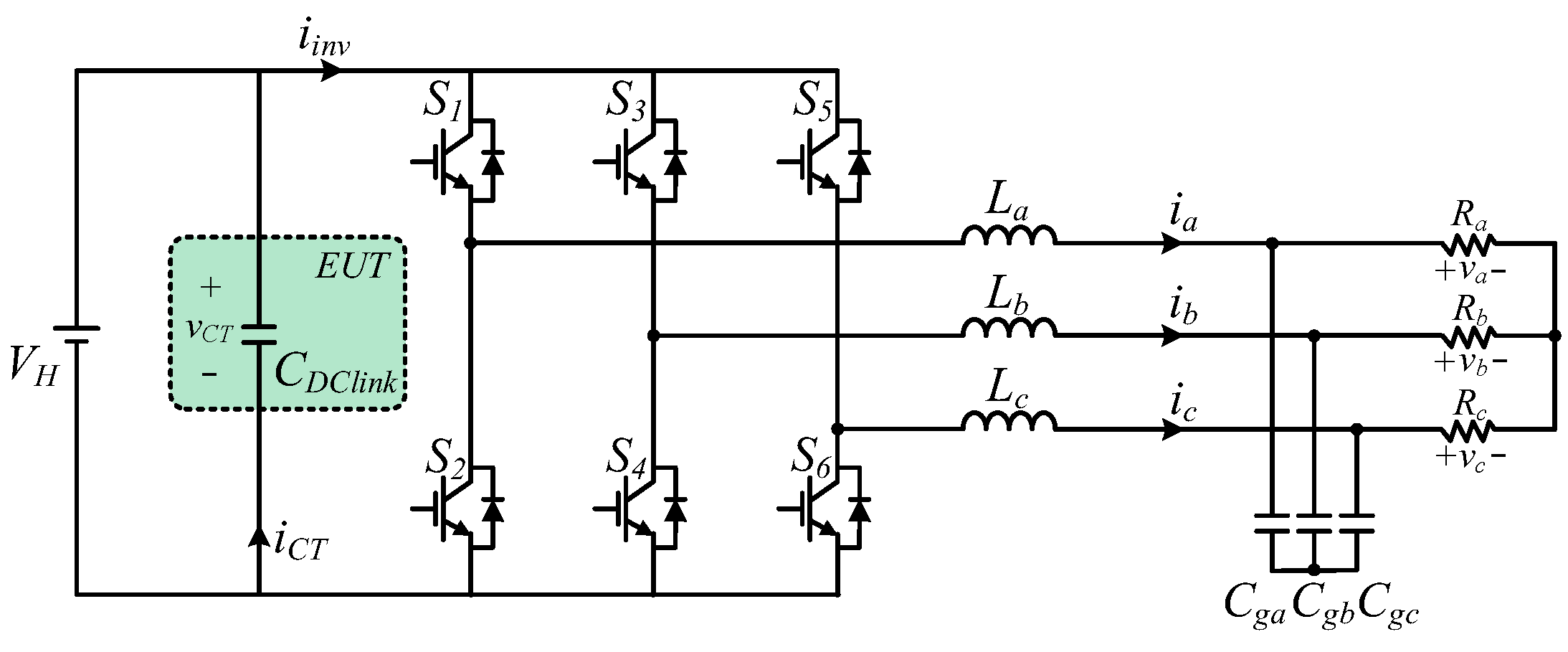
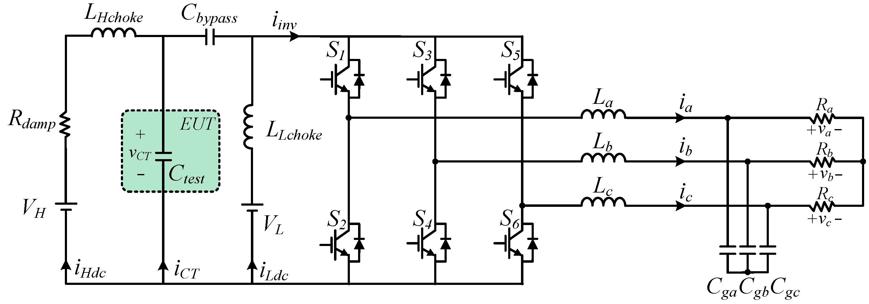
13], a small AC voltage is injected into the DC link, and the input impedance model of the inverter is adopted to simplify the measured approaches and calculate the capacitance value to realize online monitoring, which is suitable for a long-term accelerated life test. However, with the increasing power rating of inverters used in renewable energy, it will be more difficult to create a standard field to evaluate the capacitors on-line in full-scale converters and give a certification. Therefore, a down-scale capacitor evaluation testing circuit for high-power three-phase inverters was proposed in [11]. By providing a high-voltage DC source to emulate the voltage across the capacitors in a full-scale voltage rating inverter, a down-scale voltage rating inverter is used to supply the current rating, which is the same as that of a full-scale voltage rating inverter. However, in the literature [11], the inductor ripple current flowing through the capacitor is different from that in a full-scale voltage rating inverter. In addition, in practical applications, an unbalanced load in a three-phase system is a more common condition and this condition is not considered in [11], which will cause an error estimation for the capacitor operated in a high-power inverter system.
In this paper, an improved down-scale power rating evaluation system is proposed by modifying the inductor value and adding a filter in a series with a low-voltage DC supply to precisely evaluate the current of the capacitor under the test. Moreover, AC and DC analyses of the proposed improved down-scale power rating evaluation system are conducted, and the equivalent circuit and transfer function are derived. Finally, some simulation and experimental results are provided to verify the validity of the proposed down-scale evaluation system.
The remainder of this paper is organized as follows. In Section 2, the conventional down-scale evaluation system is described. Then, an improved down-scale evaluation system for the DC-link capacitors used in high-power three-phase inverter systems under balanced and unbalanced load conditions is proposed in Section 3. In Section 4, some simulation and experimental results are given to verify the validity of the proposed evaluation system. Finally, some conclusions are offered in Section 5.

2. Conventional Down-Scale System

More and more high-power three-phase inverters are widely used in renewable energy resources. Thus, the reliability of these high-power three-phase inverters becomes more and more important. A high-power full-scale three-phase inverter is shown in Figure 1, where a DC-voltage source VH is connected in the DC side and paralleled with a DC-link capacitor, which is a critical component for reliability in high-power three-phase inverters.
In order to evaluate the DC-link capacitor in a full-scale voltage rating three-phase inverter, a down-scale voltage rating evaluation system was proposed [11], as shown in Figure 2, where the voltage and current of the DC-link capacitor are designed to be very close to that of the DC-link capacitor in a full-scale voltage rating system. However, in an actual case, the down-scale inverter in Figure 2 will have different inductor current ripples in the line currents ia, ib and ic compared with the full-scale inverter in Figure 1. In addition, although the evaluation circuit can work well in a load-balanced condition, it does not perform well when the three-phase load is unbalanced. In the three-phase unbalanced load condition, the difference in the capacitor current iCT between the full-scale VSI and the evaluation circuit proposed in [11] can be observed. The main problem is that the second-order harmonic current is not high enough for the inductor LLchoke to block it. Moreover, a LC resonant circuit loop may be formed, which makes the evaluation results become worse. Therefore, in this paper, an improved down-scale evaluation circuit for DC-link capacitors in high-power applications under balanced and unbalanced load conditions is proposed and analyzed to precisely evaluate the DC-link capacitor in a high-power three-phase inverter system.

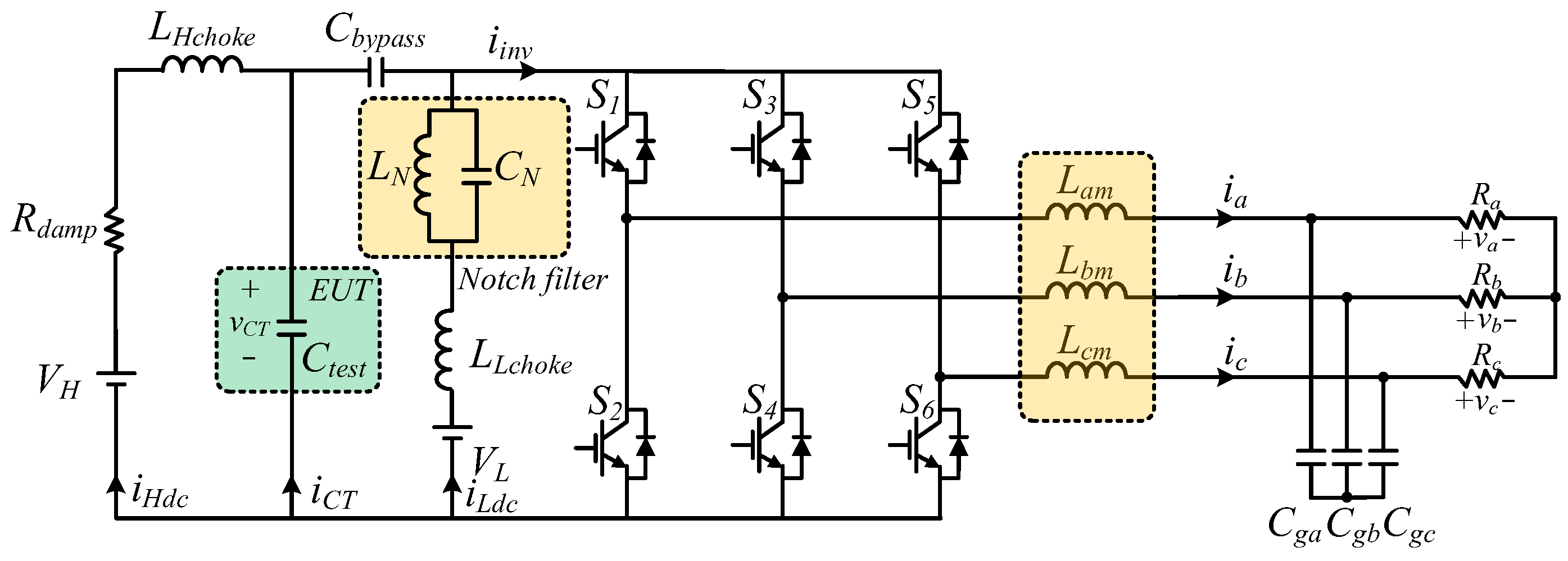
3. Proposed System Configuration

In [11], since the current rating of the small inverter is controlled to be same as that of the full-scale inverter, the relationship between the power rating of the small inverter Psmall and the full-scale inverter PFS is given by
P s m a l l P F S = V D C l i n k - S V D C l i n k - F S = V L V V H V ,
where VDClink-S and VDClink-FS are the DC-link voltages of the down-scale inverter and the full-scale inverter, respectively. However, the different DC-link voltages will change the actual inductor current ripples of the three-phase currents ia, ib and ic. The voltage across the output inductors in the down-scale voltage rating inverter is different from that in the full-scale voltage rating inverter. Therefore, the DC-link capacitor current in the down-scale voltage rating inverter is also different from that in the full-scale voltage rating inverter. In this paper, an improved evaluation circuit is proposed in Figure 3. To reach the same encountered amplitude of the current ripple in the line currents ia, ib and ic in the full-scale inverter, the inductor value should be modified according to the down-scale voltage rating as follows.
v l = L d i l d t ,
where the v l is the inductor terminal voltage, and i l is the inductor current. For example, if the low-voltage DC supply VL is half of the high-voltage DC supply VH, the inductance of the down-scale voltage rating inverter must be half the inductance of the full-scale voltage rating inverter. Otherwise, the amplitude of the current ripples in the three-phase currents in the down-scale voltage rating inverter will be half of that in the full-scale voltage rating inverter. It should be noticed that the more we lower the voltage rating of the small inverter, the smaller inductance of the output inductors we should select.
Therefore, an improved down-scale voltage rating evaluation system for DC-link capacitor is proposed in Figure 3. Compared with Figure 2, the three-phase inductors are changed and a notch filter is adopted in the low-voltage DC supply path. It should be noticed that, in order to block the high-frequency ripple current produced by the PWM inverter to flow through the high-voltage DC supply VH and low-voltage DC supply VL, the reactance of the two choke inductors must be much larger than that of Ctest and Cbypass, as follows
ω L c h o k e 1 ω C t e s t ,
where ω = 2 π f s w , f s w is the switching frequency of the inverter. LHchoke and LLchoke are the choke inductors of the high- and low-voltage DC supplies, respectively. However, under the unbalanced load condition, there exists a double-line frequency in the DC-link capacitor. The choke inductor cannot block the double-line frequency caused by the unbalanced load condition. Hence, the LN and CN must satisfy the following
1 L N C N = 2 ω l ,
where ω = 2 π f l , f l is the line frequency.
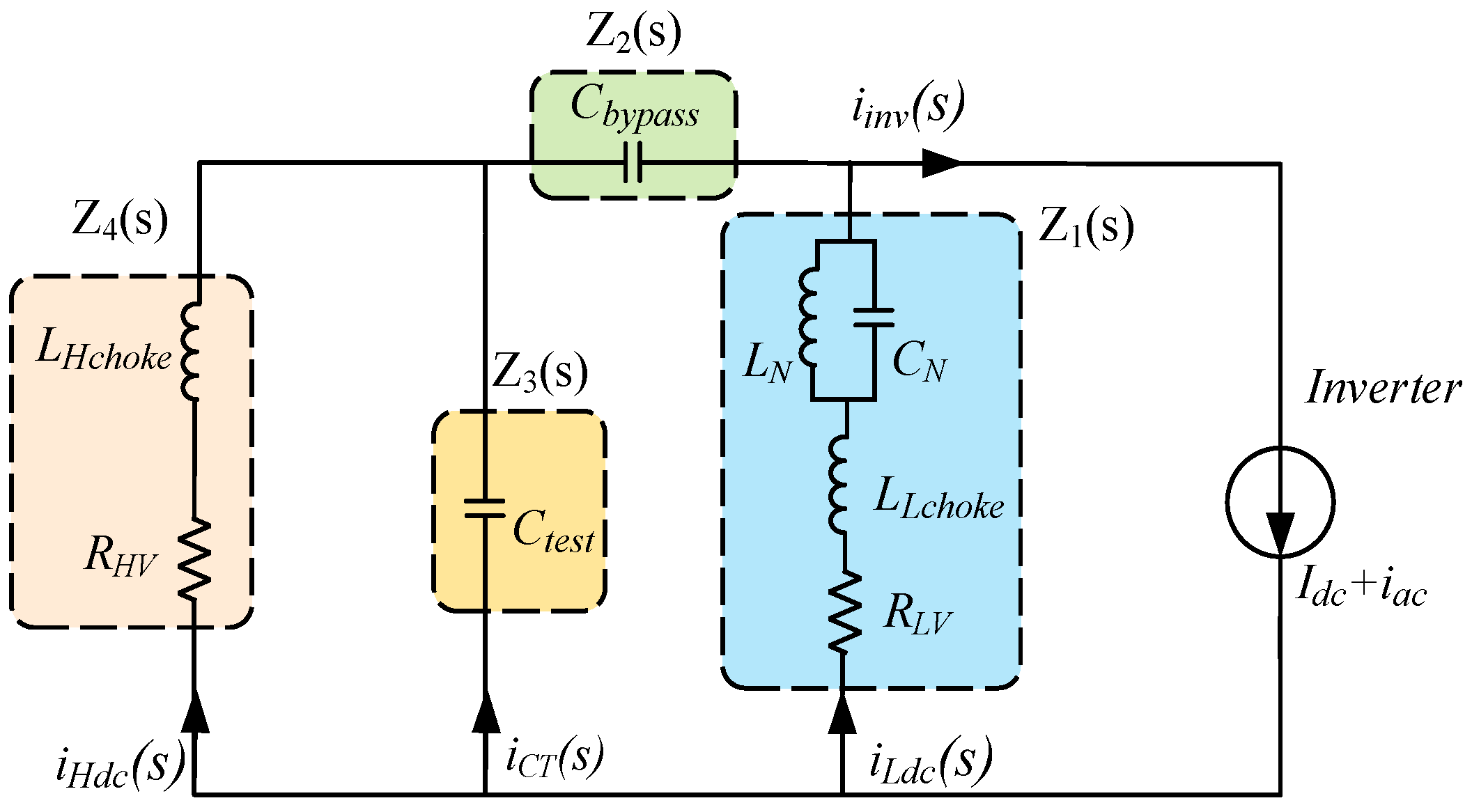
In order to analyze the proposed evaluation system shown in Figure 3, an equivalent circuit focusing on the inverter current iinv and DC side currents is introduced in Figure 4, where the low-voltage DC supply VH and high-voltage DC supply VL are set to zero. The current iinv can be seen as the current source and expressed as the sum of the DC component Idc and the AC component iac. The AC current iac includes high- and low-frequency components. The LLchoke and LHchoke are the choke inductors in the low-voltage DC side and high-voltage DC side, respectively. The RLV and RHV are the equivalent series resistance corresponding to the low-voltage DC side and the high-voltage DC side circuit branches, respectively. Note that the damping resistor Rdamp is added into the RHV. For the convenience of discussion, we assume Z1 and Z4 are the total impedance in the low-voltage DC side and the high-voltage DC side circuit branches, respectively. The Z2 and Z3 are the impedance of the bypassing capacitor Cbypass and capacitor Ctest under test, respectively. Therefore, the impedances Z1 to Z4 can be written as follows:
Z 1 ( s ) = s L N s 2 L N C N + 1 + s L L c h o k e + R L V ,
Z 2 ( s ) = 1 s C b y p a s s ,
Z 3 ( s ) = 1 s C t e s t ,
Z 4 ( s ) = s L H c h o k e + R H V ,
Then the transfer functions G1(s) from iinv to iLdc, and G2(s) from iinv to iCT can be expressed as follows
G 1 ( s ) = i L d c ( s ) i i n v ( s ) = Z 2 ( Z 3 + Z 4 ) + Z 3 Z 4 Z 3 Z 4 + ( Z 1 + Z 2 ) ( Z 3 + Z 4 ) ,
G 2 ( s ) = i C T ( s ) i i n v ( s ) = Z 1 Z 4 Z 3 Z 4 + ( Z 1 + Z 2 ) ( Z 3 + Z 4 ) ,
Under the load-unbalanced condition, the AC component iac in the current iinv contains a second-order harmonic current and a high-frequency switching current, which are greater than or equal to 120 Hz. It should be noted that, when the current frequency is 120 Hz or above, the impedance of Z3 is much smaller than Z4. For instance, if the current frequency is 120 Hz and the capacitor Ctest, choke inductor LHchoke, and equivalent series resistance RHV are selected as 2.2 mF, 1.6 mH and 10 ohm, respectively, the impedance Z3 is 0.6 ohm and Z4 is 11.2 ohm. In this condition, Z3 is much less than Z4. Thus, for AC components above 120 Hz in current iinv, Z4 can be approximated as an open circuit. Thus, the transfer functions from iac to iLdc, and from iac to iCT can be written as follows, respectively.
G 3 ( s ) = i L d c ( s ) i a c ( s ) = Z 2 + Z 3 Z 1 + Z 2 + Z 3 ,
G 4 ( s ) = i C T ( s ) i a c ( s ) = Z 1 Z 1 + Z 2 + Z 3 ,
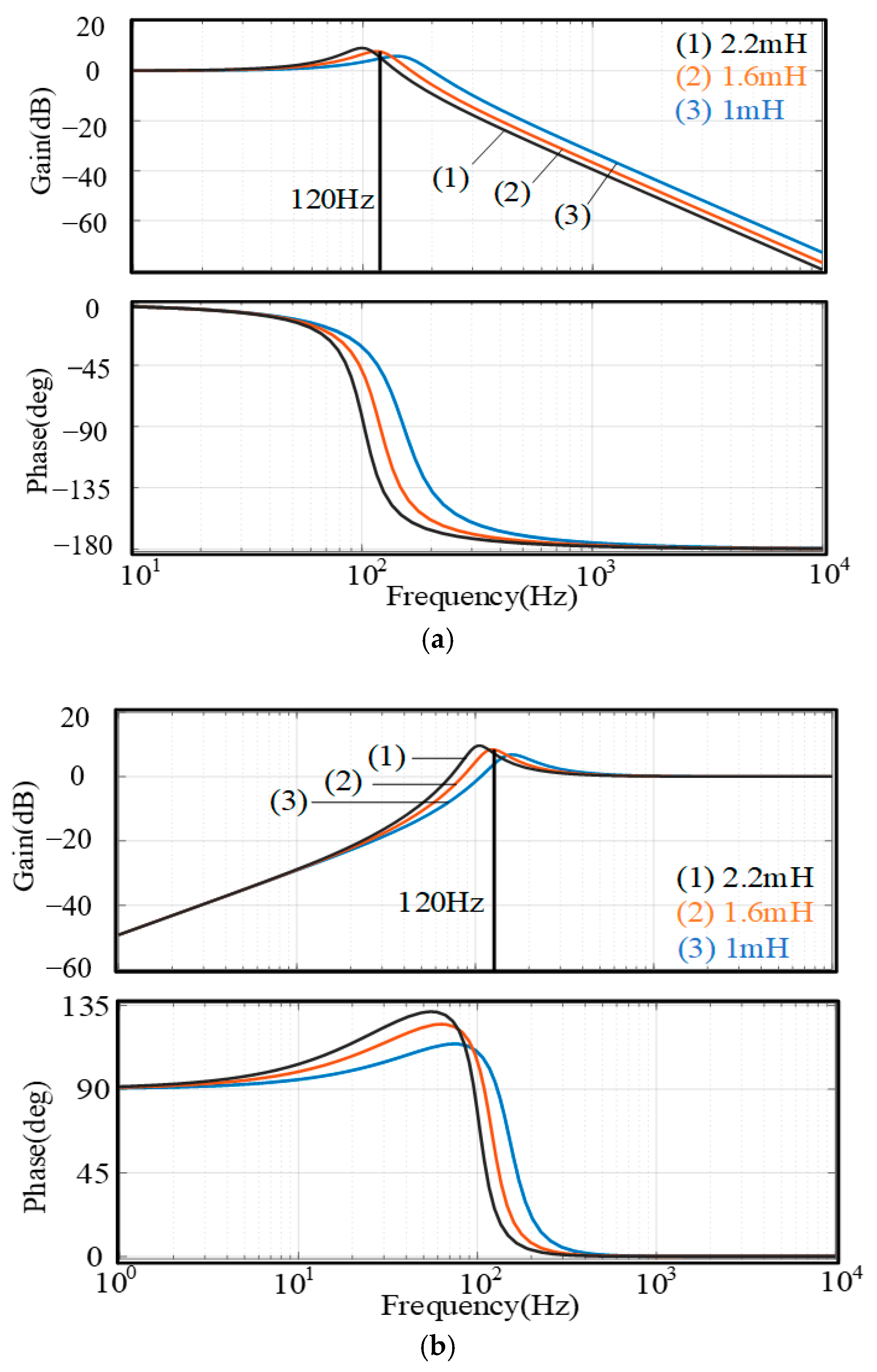
In order to discuss the properties of the conventional and proposed evaluation systems for capacitors utilized in high-power three-phase inverters, G3(s) and G4(s) in the evaluation system [11] can be written as Equations (13) and (14)
i L d c ( s ) i a c ( s ) = 1 s 2 L L c h o k e C S + s R L V C S + 1 ,
i C T ( s ) i a c ( s ) = s 2 L L c h o k e C S + s R L V C S s 2 L L c h o k e C S + s R L V C S + 1 ,
where CS is the equivalent series capacitor in the Z2 and Z3 circuit branch. In the following, the choke inductor LLchoke is discussed under three different inductor values, namely 1 mH, 1.6 mH, and 2.2 mH. The bode plots of G3 and G4 in the conventional evaluation system are shown in Figure 5a,b, respectively. Note that, in the system, CS and LLchoke will form an LC resonant circuit. For the worst case, when the inductance value of the choke inductor LLchoke is 1.6 mH, the second-order harmonic current, i.e., 120 Hz, will exactly fall on the peak resonance, where the gain of the transfer function is at the maximum. In this case, it will seriously influence the current iCT under test because the second-order current will not only flow into iLdc, but also be amplified due to the LC resonance. To solve this problem, a filter is adopted and added to the low DC voltage side circuit branch, shown in 
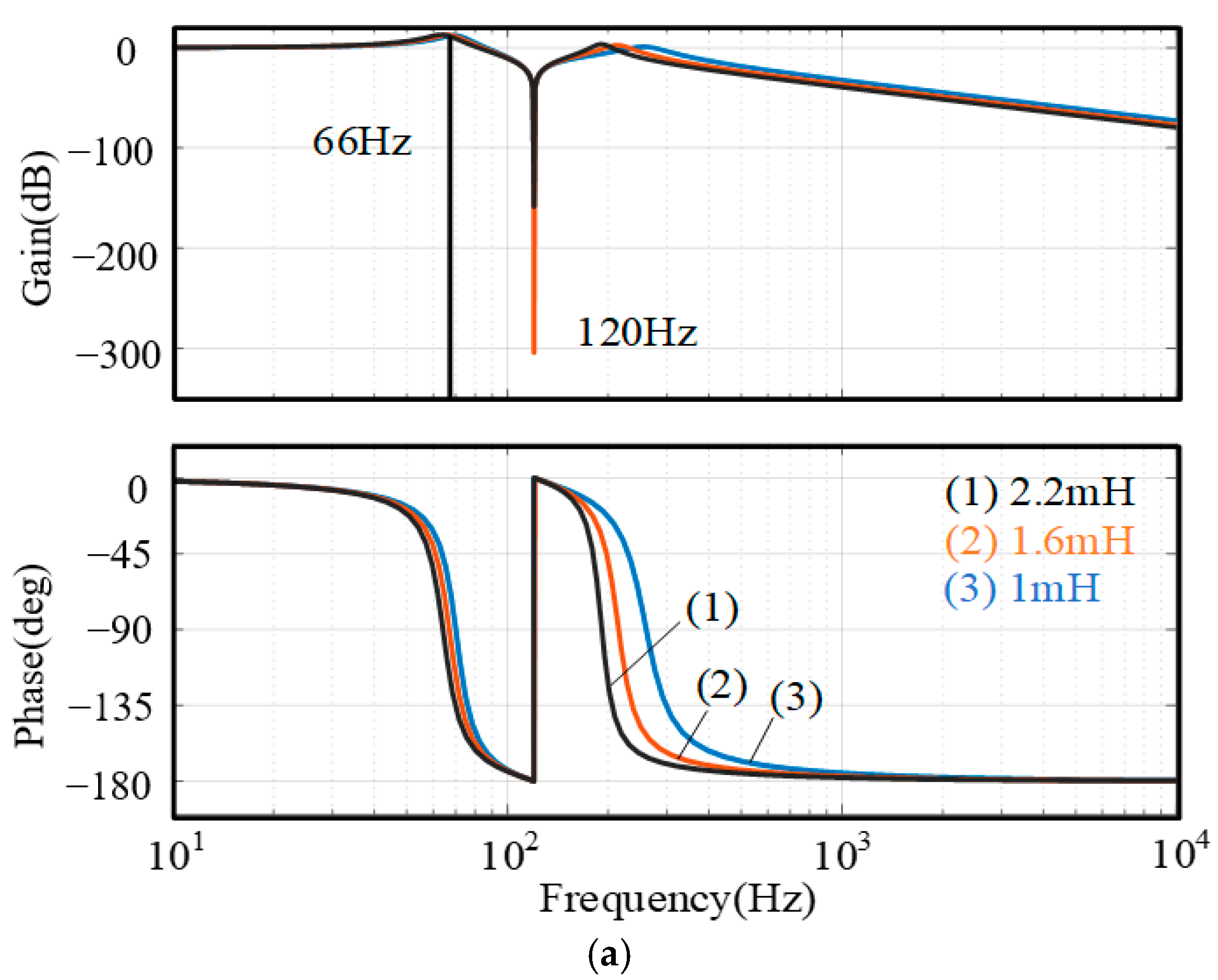
Figure 3, to block the second-order harmonic current and change the resonance situation. For the improved system in this paper, G3(s) and G4(s) are given as Equations (15) and (16), respectively. The bode plots of G3(s) and G4(s) in the improved evaluation system are shown in Figure 6. Different from that shown in Figure 5, the gain of the transfer function G3(s) at 120 Hz is much smaller. Thus, it can be seen from Figure 5 and Figure 6 that, for the 120 Hz ripple current, the impedance of Z1 is high enough to block it. Moreover, the peak resonance point is set to 66 Hz, as shown in Figure 6a. Note that, under the load-unbalanced condition, iac does not contain the ripple currents whose frequencies are below 120 Hz. Figure 6b shows the bode plot of the transfer function G4(s). No matter what inductance value of LLchoke is selected, the gain of G4(s) stays at 0 dB at 120 Hz and at the switching frequency, which indicates that the AC component of the capacitor current iCT is equal to the ripple current flowing from the down-scale and full-scale voltage rating inverter under the unbalanced load condition.
i L d c ( s ) i a c ( s ) = s 2 L N C N + 1 s 4 L L c h o k e C S L N C N + s 3 R L V C S L N C N + s 2 ( L N C N + L L c h o k e C S + L N C S ) + s R L V C S + 1 ,
i C T ( s ) i a c ( s ) = s 4 L L c h o k e C S L N C N + s 3 R L V C S L N C N + s 2 ( L L c h o k e C S + L N C S ) + s R L V C S s 4 L L c h o k e C S L N C N + s 3 R L V C S L N C N + s 2 ( L N C N + L L c h o k e C S + L N C S ) + s R L V C S + 1 ,

4. Simulation and Experimental Results

To verify the effectiveness of the proposed evaluation system, some simulation results are executed. Simultaneously, a full-scale voltage rating inverter and a down-scale voltage rating evaluation system are also constructed. Table 1 and Table 2 list the circuit parameters of the full-scale voltage rating inverter and the down-scale voltage rating evaluation systems used in the simulation and experiment, respectively.
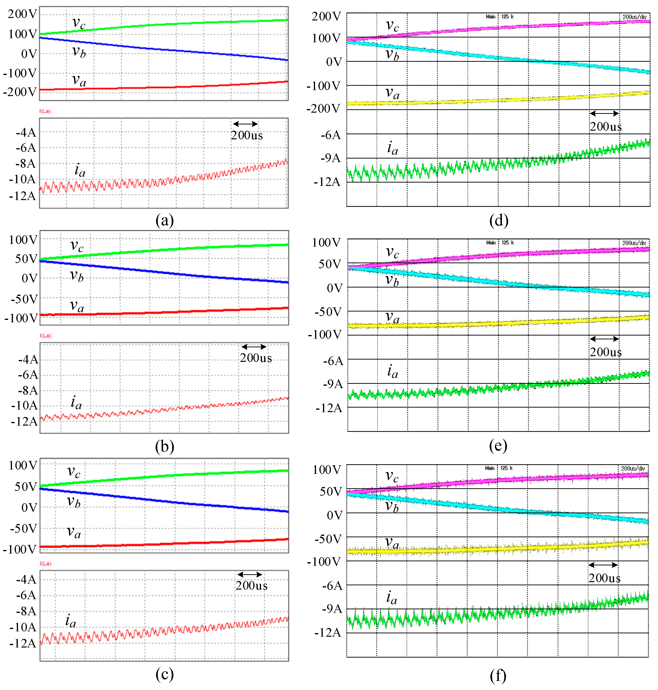
Figure 7a–c and Figure 7d–f shows the simulation and experimental results of the output voltages Va, Vb, Vc, and the output inductor current ia, respectively. Due to the power rating of the down-scale voltage rating VSI being half that of the full-scale voltage rating VSI, it can be seen from Figure 7 that the output inductor values of the down-scale voltage rating VSI must be modified to half that of the full-scale voltage rating VSI, so that the amplitude of the line current ripple in the down-scale voltage rating inverter is very close to that in the full-scale inverter. Table 3 and Table 4 show the simulated and measured peak-to-peak current ripples at the maximum phase voltage, respectively. As can be observed from Table 3 and Table 4, one can see that the amplitude of the current ripple in the proposed down-scale voltage rating evaluation system has a value closer to that of the full-scale voltage rating VSI, when compared with the conventional down-scale voltage rating evaluation system.
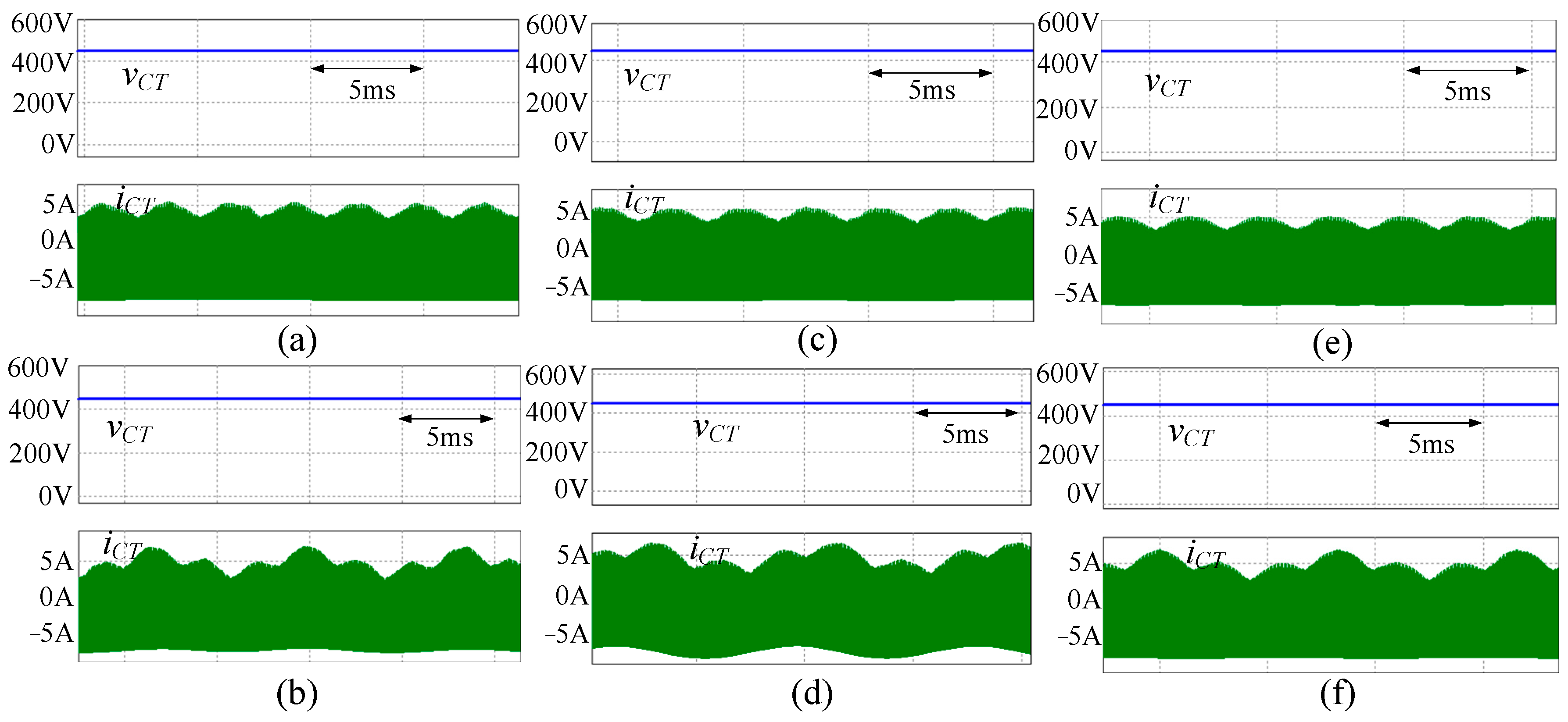
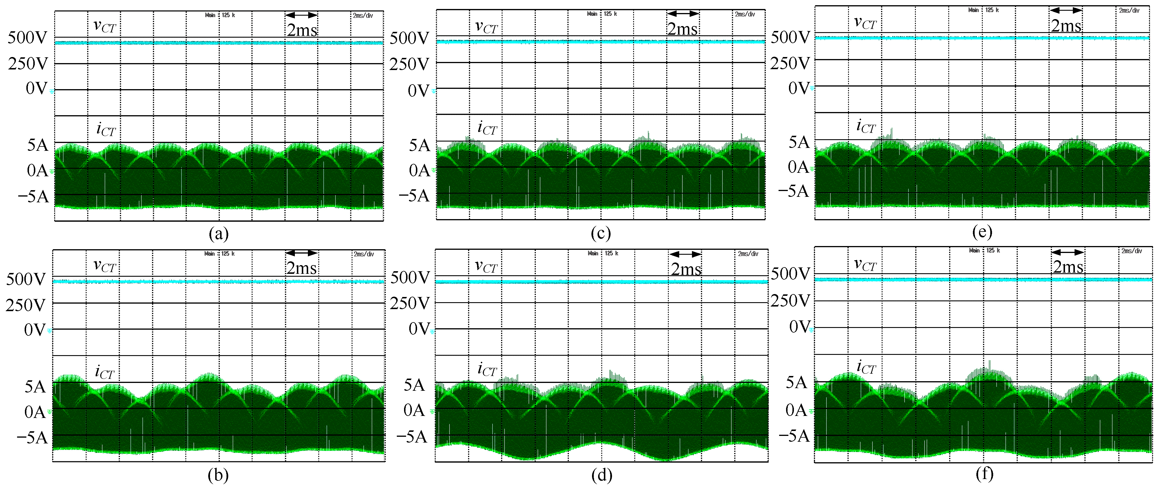
Figure 8 shows the voltage and current simulated waveforms of the capacitor under test in the full-scale voltage rating inverter, conventional down-scale voltage rating evaluation system, and proposed down-scale voltage rating evaluation system. Figure 8a,b illustrates the simulated waveforms of the full-scale voltage rating inverter under the load-balanced and load-unbalanced conditions, respectively. As shown in Figure 8c,d, although the testing capacitor current iCT of the conventional down-scale voltage rating evaluation system can be very close to that of the full-scale voltage rating inverter in the load-balanced condition, it does not perform well in the load-unbalanced condition. By comparison, the proposed down-scale voltage rating evaluation system can have a similar testing capacitor current iCT compared with the conventional down-scale voltage rating evaluation system in both the load-balanced and load-unbalanced conditions, as shown in Figure 8e,f.
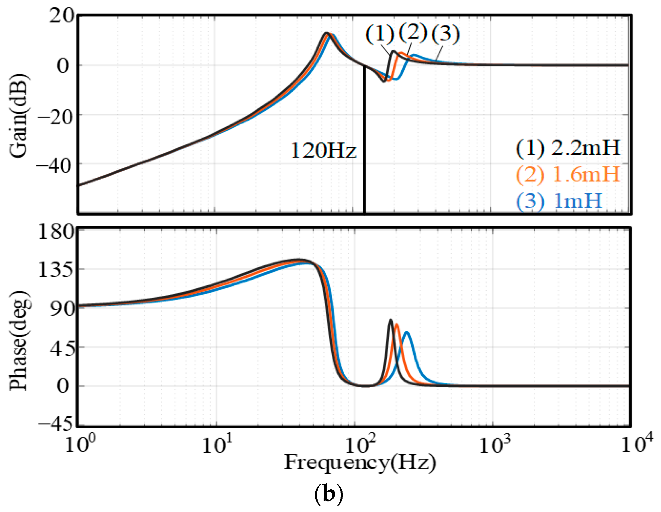
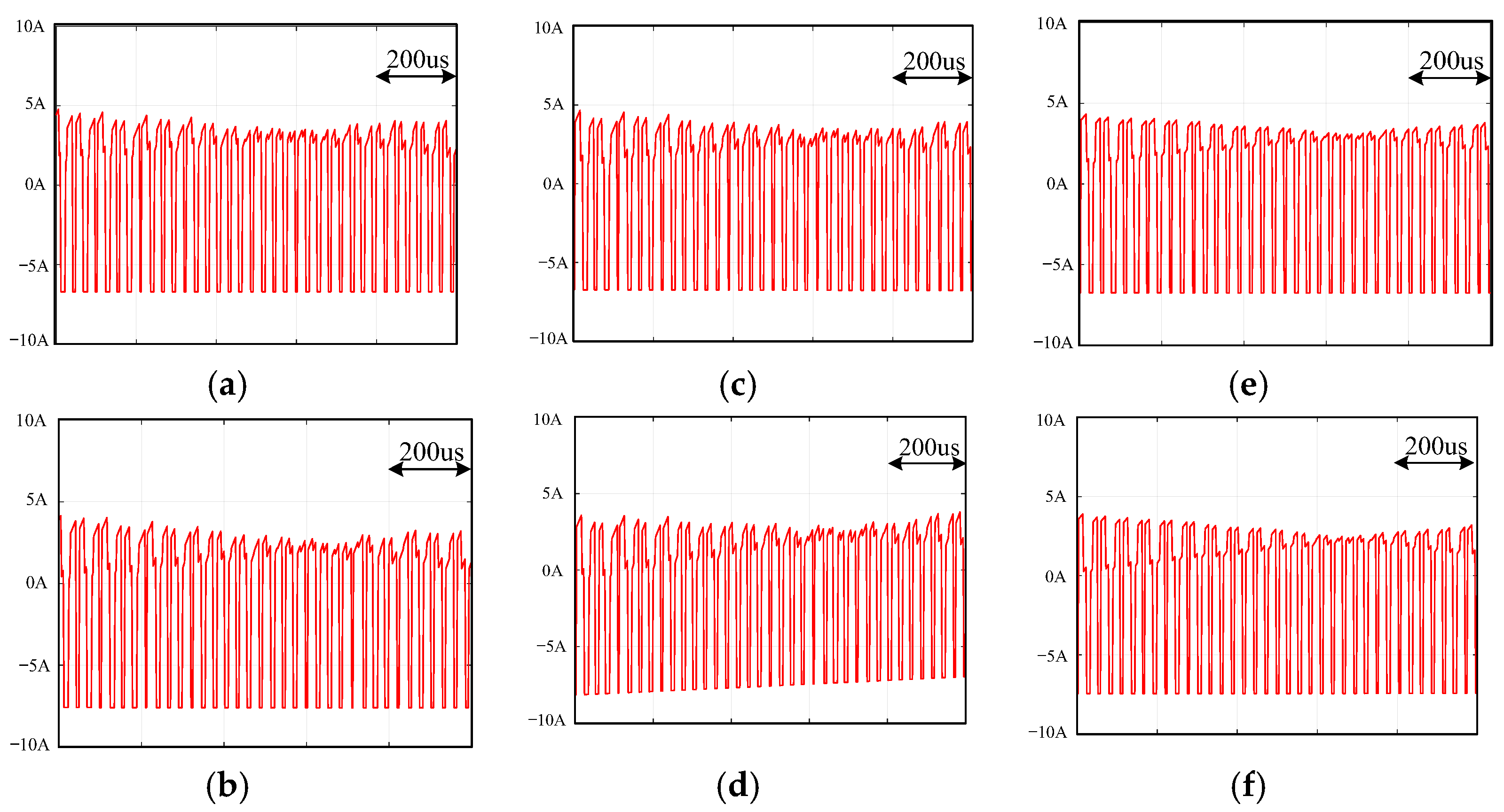
In order to clarify the difference in the capacitor evaluation results, the corresponding enlarged view of the simulated current iCT of the DC-link capacitor under test is illustrated in Figure 9. It follows from 
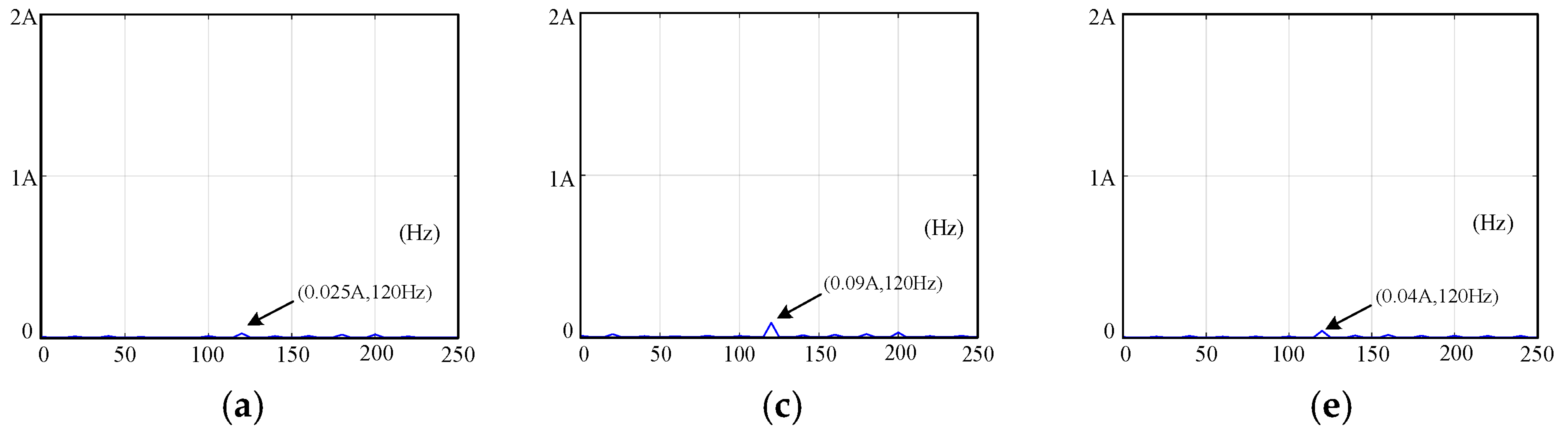
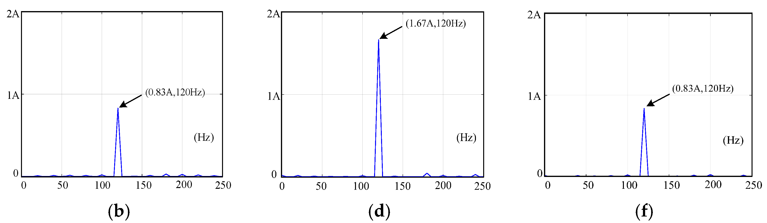
Figure 9 that, under the balanced load condition, the conventional and proposed down-scale evaluation systems can obtain a similar DC-link capacitor current under test compared with the full-scale voltage rating VSI, but it is different under the unbalanced load condition. In addition, the corresponding close-to-120 Hz FFT results of the simulated iCT of the DC-link capacitor under test are shown in Figure 10. As can be seen from Figure 10, under the balanced load condition, the amplitude of the double-line frequency in the full-scale voltage rating VSI, conventional down-scale voltage rating evaluation system, and proposed down-scale voltage rating evaluation system is very close to zero. However, under the unbalanced load condition, the amplitude of the double-line frequency in the conventional down-scale voltage rating evaluation system is much different from that in the full-scale voltage rating VSI.
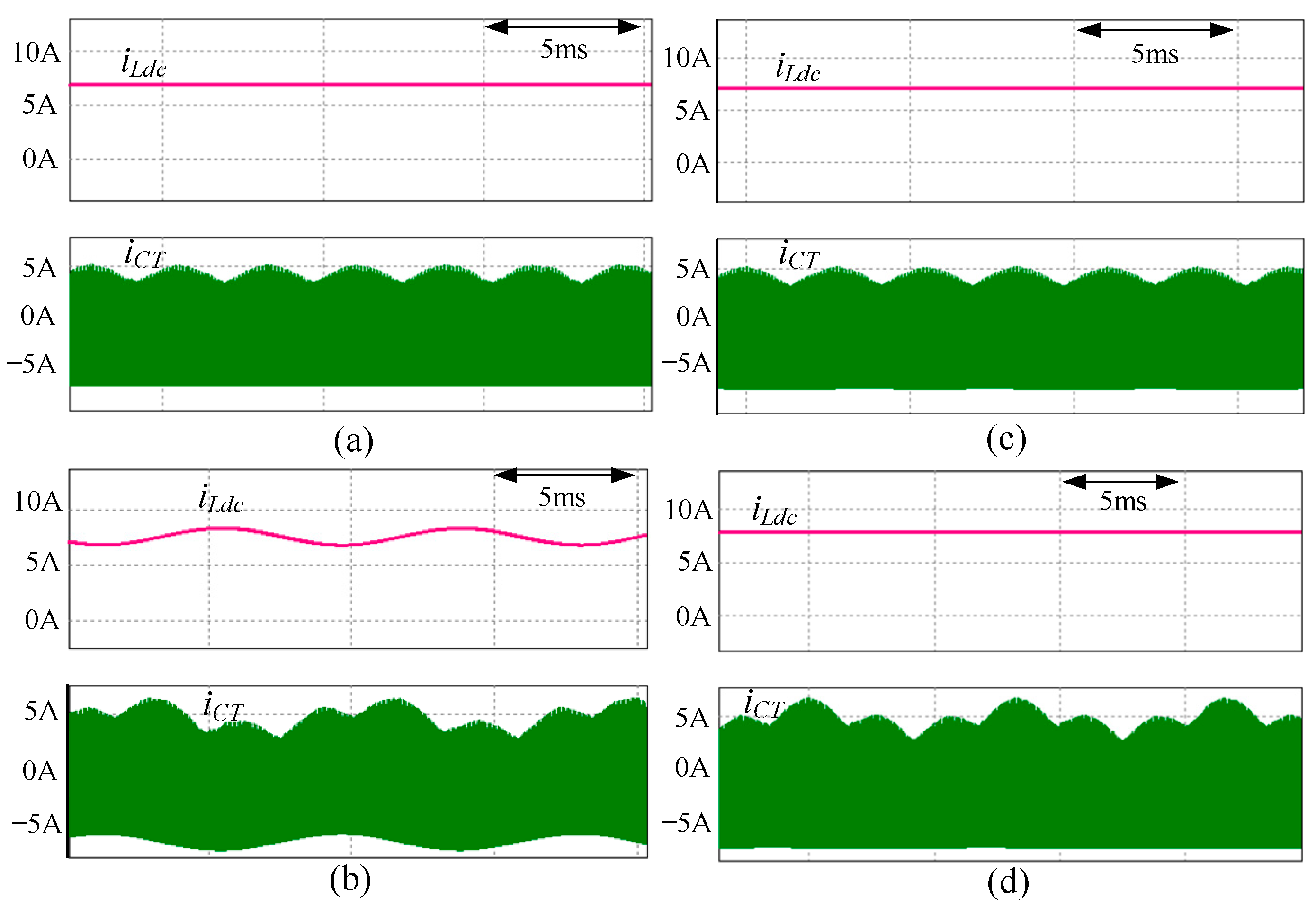
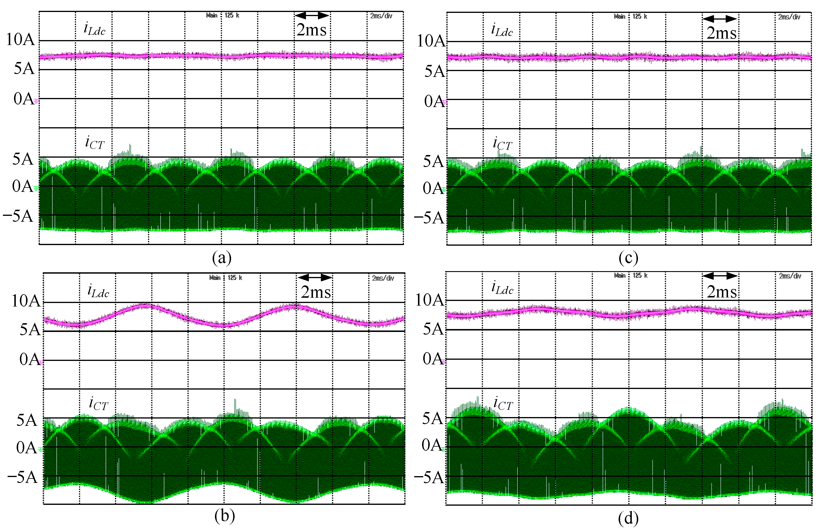
Next, by analyzing the iLdc and iCT, one can observe the problem of the previous system [11] in Figure 11. Figure 11b shows that, when the three phase loads are unbalanced, the double-line frequency or second-order harmonic current will flow into iLdc and be amplified by an LC resonant circuit loop. As shown in Figure 11d, the proposed down-scale voltage rating evaluation system can block the second-order harmonic current in the low-voltage DC-side iLdc circuit branch and change the LC resonant circuit loop. Figure 12 and Figure 13 are the experimental results corresponding to the simulation results in Figure 8 and Figure 11, respectively. As can be observed from Figure 8, Figure 11, Figure 12 and Figure 13, the experimental results are in very close agreement with the simulation results. Both the simulation and experimental results verify the validity of the proposed down-scale voltage rating evaluation system.

5. Conclusions

More and more high-power and high-density inverters are manufactured for renewable energy systems to reduce carbon emissions in the world. Therefore, the system testing and certification for high-power and high-density inverters becomes very important, especially in the limited power rating testing field. In order to reproduce the same encountered stresses when a DC-link capacitor is used in a high-power inverter with pulse-width modulation, in this article, an improved evaluation circuit for the DC-link capacitors used in high-power three-phase inverters under balanced and unbalanced load conditions is proposed. A comparison of the down-scale voltage rating evaluation systems is analyzed and some problems in the conventional evaluation systems are discovered. It was found that, under an unbalanced load condition, the conventional down-scale voltage rating evaluation system does not present very closely the testing capacitor current of the full-scale voltage rating inverter system. In order to more precisely evaluate the current of the capacitor under test, the output inductors of the conventional evaluation system are modified, and a filter is added in the low-voltage DC-side circuit branch. From the simulation and experimental results, the proposed down-scale voltage rating evaluation system presents the closest ripple current waveform and DC bias voltage of the DC-link capacitors in the full-scale voltage rating inverter system under the balanced and unbalanced load conditions. The validity of the proposed down-scale voltage rating evaluation system is verified in this article. In the future, the accelerated life testing of capacitors working in severely adverse circumstances can be utilized in the proposed improved down-scale voltage rating evaluation system.

Author Contributions

Conceptualization, Y.-H.L.; methodology, Y.-L.L.; validation, Y.-H.L. The paper was a collaborative effort among the authors. The authors contributed collectively to the theoretical analysis, modeling, simulation, experiment, and manuscript preparation. All authors have read and agreed to the published version of the manuscript.

Funding

This research was funded by [the Ministry of Science and Technology of R.O.C] grant number [111-3116-F-008-003].

Data Availability Statement

Not applicable.

Conflicts of Interest

The authors declare no conflict of interest.

References

  1. IEC 60364-7-712:2017; Requirements for Special Installations or Locations—Solar Photovoltaic (PV) Power Supply Systems. International Electrotechnical Commission: Geneva, Switzerland, 2017.
  2. IEC 61000-3-3:2013+AMD1:2017+AMD2:2021 CSV; Electromagnetic Compatibility (EMC)—Part 3-3: Limits—Limitation of Voltage Changes, Voltage Fluctuations and Flicker in Public Low-Voltage Supply Systems, for Equipment with Rated Current ≤16 A Per Phase and Not Subject to Conditional Connection. International Electrotechnical Commission: Geneva, Switzerland, 2021.
  3. IEC/TS 61000-3-4; Electromagnetic Compatibility (EMC)—Part 3-4: Limits—Limitation of Emission of Harmonic Currents in Low-Voltage Power Supply Systems for Equipment with Rated Current Greater Than 16 A. International Electrotechnical Commission: Geneva, Switzerland, 1998.
  4. Amaral, A.M.R.; Cardoso, A.J.M. A simple offline technique for evaluating the condition of aluminum–electrolytic–capacitors. IEEE Trans. Ind. Electron. 2009, 56, 3230–3237. [Google Scholar] [CrossRef]
  5. Amaral, A.M.R.; Cardoso, A.J.M. Estimating aluminum electrolytic capacitors condition using a low frequency transformer together with a DC power supply. In Proceedings of the 2010 IEEE International Symposium on Industrial Electronics, Bari, Italy, 4–7 July 2010; pp. 815–820. [Google Scholar]
  6. Wang, H.; Blaabjerg, F. Reliability of capacitors for dc-ink applications in power electronic converters—An overview. IEEE Trans. Ind. Appl. 2014, 50, 3569–3578. [Google Scholar] [CrossRef]
  7. Ondel, O.; Boutleux, E.; Venet, P. A decision system for electrolytic capacitors diagnosis. In Proceedings of the 2004 IEEE 35th Annual Power Electronics Specialists Conference, Aachen, Germany, 20–25 June 2004; pp. 4360–4364. [Google Scholar]
  8. Makdessi, M.; Sari, A.; Venet, P. Metallized polymer film capacitors ageing law based on capacitance degradation. Microelectron. Reliab. 2014, 54, 1823–1827. [Google Scholar] [CrossRef]
  9. Wu, Y.; Du, X. A VEN Condition Monitoring Method of DC-Link Capacitors for Power Converters. IEEE Trans. Ind. Electron. 2019, 66, 1296–1306. [Google Scholar] [CrossRef]
  10. Zhou, W.; Wang, M.; Wu, Q.; Xi, L.; Xiao, K.; Bhat, K.P.; Chen, C.C. Accelerated Life Testing Method of Metallized Film Capacitors for Inverter Applications. IEEE Trans. Transp. Electrif. 2021, 7, 37–49. [Google Scholar] [CrossRef]
  11. Hasegawa, K.; Omura, I.; Nishizawa, S.I. Design and Analysis of a New Evaluation Circuit for Capacitors Used in a High-Power Three-Phase Inverter. IEEE Trans. Ind. Electron. 2016, 63, 2679–2687. [Google Scholar] [CrossRef]
  12. Chroma ATE Inc. Ripple Current Tester Model 11800/11801/11810. 2022. Available online: https://assets.testequity.com/te1/Documents/pdf/11800-ds.pdf (accessed on 18 September 2022).
  13. Makdessi, M.; Sari, A.; Venet, P.; Bevilacqua, P.; Joubert, C. Accelerated ageing of metallized film capacitors under high ripple currents combined with a DC voltage. IEEE Trans. Power Electron. 2015, 30, 2435–2444. [Google Scholar] [CrossRef]
  14. Li, H.; Xiang, D.; Han, X.; Zhong, X.; Yang, X. High-accuracy capacitance monitoring of DC-link capacitor in VSI systems by LC resonance. IEEE Trans. Power Electron. 2019, 34, 12200–12211. [Google Scholar] [CrossRef]
Figure 1. Full-scale voltage rating evaluation system in a high-power three-phase inverter.
Energies 15 06937 g001
Figure 2. Down-scale voltage rating evaluation system in a high-power three-phase inverter [11].
Energies 15 06937 g002
Figure 3. Proposed down-scale voltage rating evaluation system.
Energies 15 06937 g003
Figure 4. Equivalent circuit focusing on the current flowing into the inverter iinv, capacitor current iCT, high voltage DC current iHdc, and low voltage DC current iLdc.
Energies 15 06937 g004
Figure 5. Bode plot of the transfer function in evaluation system proposed in [11]. (a) G3(s). (b) G4(s).
Energies 15 06937 g005
Figure 6. Bode plot of the transfer function proposed in this paper. (a) G3(s). (b) G4(s).
Energies 15 06937 g006aEnergies 15 06937 g006b
Figure 7. Simulation (left) and corresponding experimental (right) waveforms of output three-phase voltages Va, Vb, Vc and output current ia under (a,d) full-scale VSI with output inductor 2 mH, (b,e) conventional down-scale voltage rating evaluation system with output inductor 2 mH, and (c,f) proposed down-scale voltage rating evaluation system with output inductor 1 mH.
Energies 15 06937 g007
Figure 8. The simulated voltage vCT and current iCT of the DC-link capacitor under test for (a,c,e) balanced and (b,d,f) unbalanced load condition in the (a,b) full-scale voltage rating VSI, (c,d) conventional down-scale voltage rating evaluation system, and (e,f) proposed down-scale voltage rating evaluation system.
Energies 15 06937 g008
Figure 9. The enlarged view of simulated current iCT of the DC-link capacitor under test for (a,c,e) balanced and (b,d,f) unbalanced load conditions in the (a,b) full-scale voltage rating VSI (c,d), conventional down-scale voltage rating evaluation system, and (e,f) the proposed down-scale voltage rating evaluation system.
Energies 15 06937 g009
Figure 10. Close-to-120 Hz FFT results of current iCT of the DC-link capacitor under test for (a,c,e) balanced and (b,d,f) unbalanced load conditions in the (a,b) full-scale voltage rating VSI, (c,d) conventional down-scale voltage rating evaluation system, and (e,f) proposed down-scale voltage rating evaluation system.
Energies 15 06937 g010aEnergies 15 06937 g010b
Figure 11. The simulated waveforms of the low-voltage-side dc current iLdc and the testing capacitor current iCT for (a,c) balanced and (b,d) unbalanced load conditions in the (a,b) conventional down-scale voltage rating evaluation system, and the (c,d) proposed down-scale voltage rating evaluation system.
Energies 15 06937 g011
Figure 12. The measured voltage vCT and current iCT of the DC-link capacitor under test for (a,c,e) balanced and (b,d,f) unbalanced load conditions in the (a,b) full-scale voltage rating VSI, (c,d) conventional down-scale voltage rating evaluation system, and (e,f) proposed down-scale voltage rating evaluation system.
Energies 15 06937 g012
Figure 13. The measured waveforms of the low-voltage-side dc current iLdc and the testing capacitor current iCT for (a,c) balanced and (b,d) unbalanced load conditions in the (a,b) conventional down-scale voltage rating evaluation system, and (c,d) proposed down-scale voltage rating evaluation system.
Energies 15 06937 g013
Table 1. Parameters of the full-scale voltage rating inverter used in simulation and experiment.
NameSymbolParameter
Power ratingP3 kW
DC link voltageVH450 V
DC link capacitorCDClink2.2 mF
AC line voltage (rms)Vline220 V
Switching frequencyfsw18 kHz
Output frequencyfo60 Hz
Output inductorsLa Lb Lc2 mH
Output capacitorsCga Cgb Cgc22 uF
Balanced load resistorsRa Rb Rc16 Ω, 16 Ω, 16 Ω
Unbalanced load resistorsRa Rb Rc12 Ω, 16 Ω, 16 Ω
Table 2. Parameters of the down-scale voltage rating evaluation system used in simulation and experiment.
NameSymbolParameter
Power rating of the systemP1.5 kW
High-DC voltage sourceVH450 V
Low-DC voltage sourceVL225 V
High-voltage choke inductorLHchoke1.6 mH
Low-voltage choke inductorLLchoke1.6 mH
Notch filter inductorLN2.43 mH
Notch filter capacitorCN0.724 mF
Bypassing capacitorCbypass2.2 mF
Capacitor under testCtest2.2 mF
Damping resistorRdamp10 Ω
AC line voltage (rms)Vline110 V
Switching frequencyfsw18 kHz
Output frequencyfo60 Hz
Output inductorsLam Lbm Lcm1 mH
Output capacitorsCga Cgb Cgc22 uF
Balanced Load resistorsRa Rb Rc8 Ω, 8 Ω, 8 Ω
Unbalanced load resistorsRa Rb Rc6 Ω, 8 Ω, 8 Ω
Table 3. Comparison of simulated line-current ripple at maximum phase voltage.
Ripple (Peak to Peak)Full-Scale VSIConventional Down-Scale Evaluation SystemProposed Down-Scale Evaluation System
Maximum~1.64 A~0.79 A~1.58 A
Table 4. Comparison of measured line-current ripple at maximum phase voltage.
Ripple (Peak to Peak)Full-Scale VSIConventional Down-Scale Evaluation SystemProposed Down-Scale Evaluation System
Maximum~2.23 A~0.88 A~2.41 A
Publisher’s Note: MDPI stays neutral with regard to jurisdictional claims in published maps and institutional affiliations.

