
A 1.2 kV SiC MOSFET with Integrated Heterojunction Diode and P-shield Region


Abstract
:1. Introduction
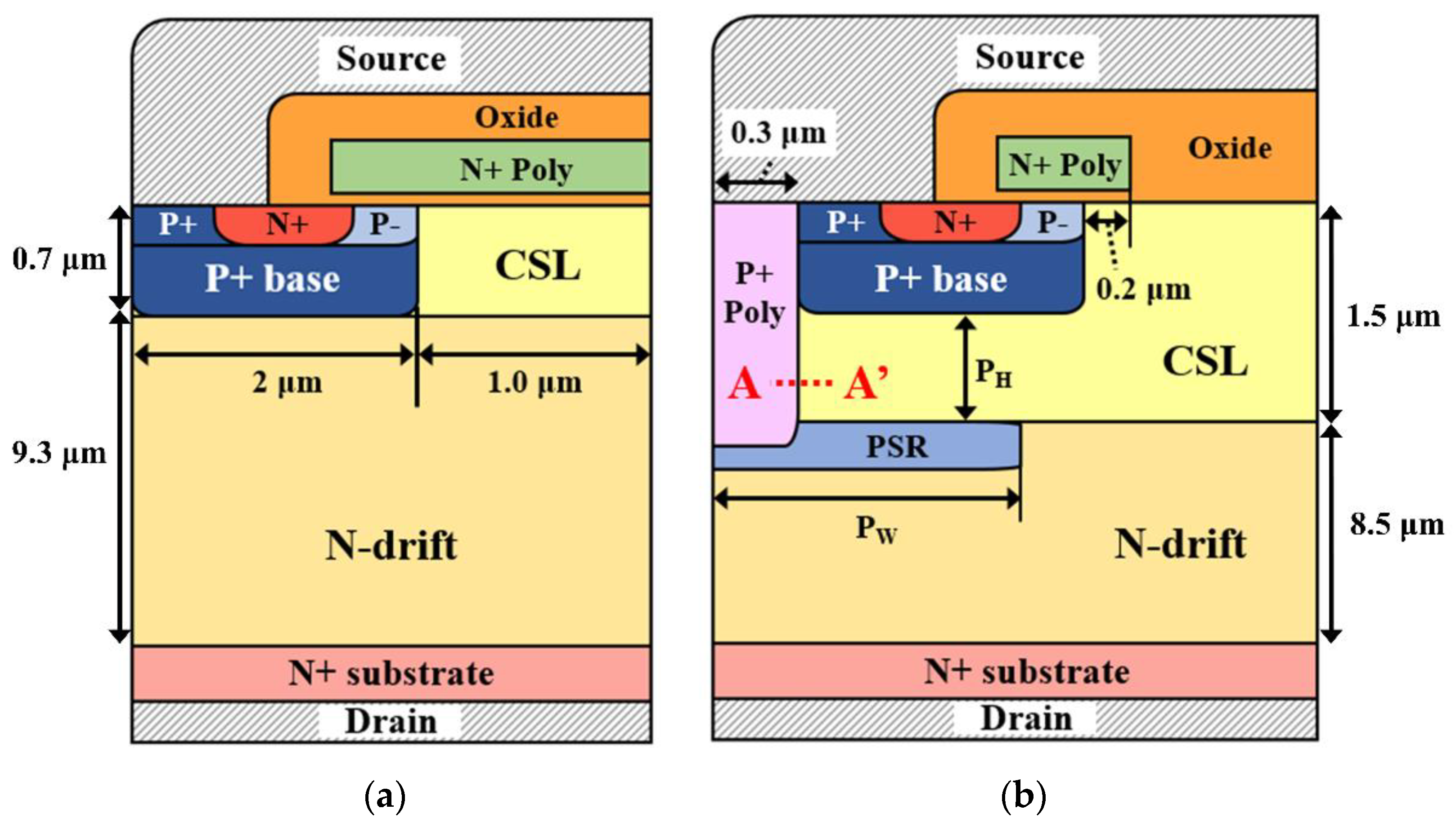
2. Device Structures and Fabrication Procedures
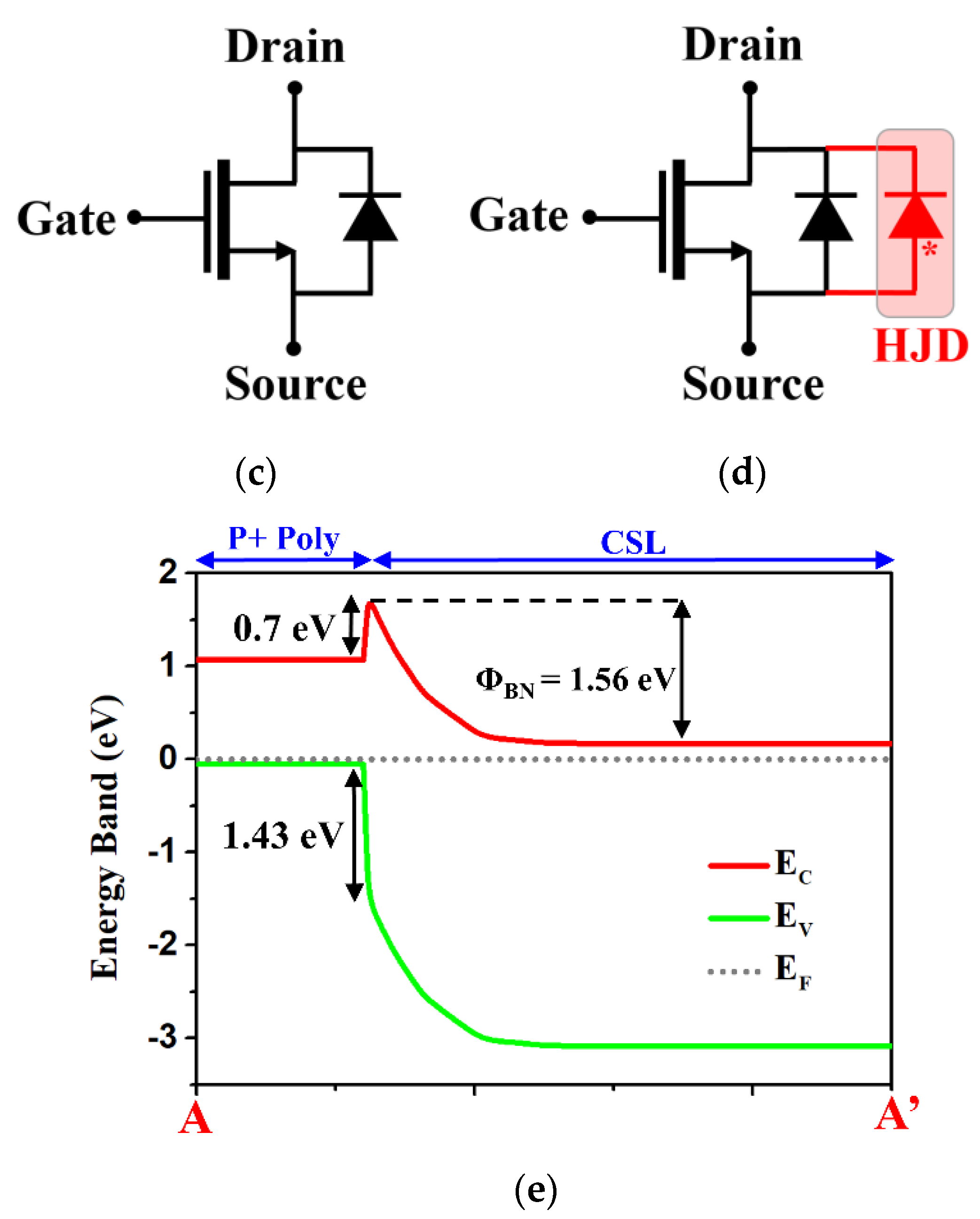
2.1. Device Structures and Concept
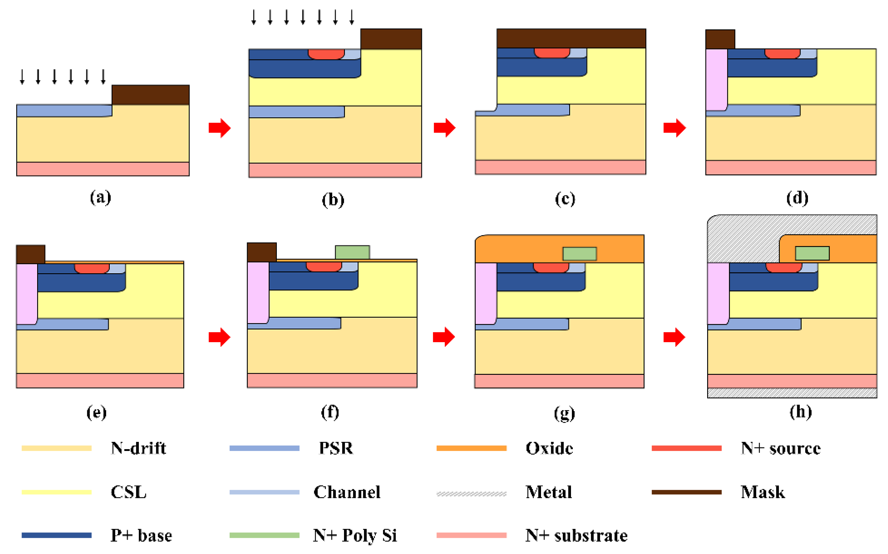
2.2. Proposed Fabrication Procedures
3. Results and Discussions
3.1. Simulation Test Conditions
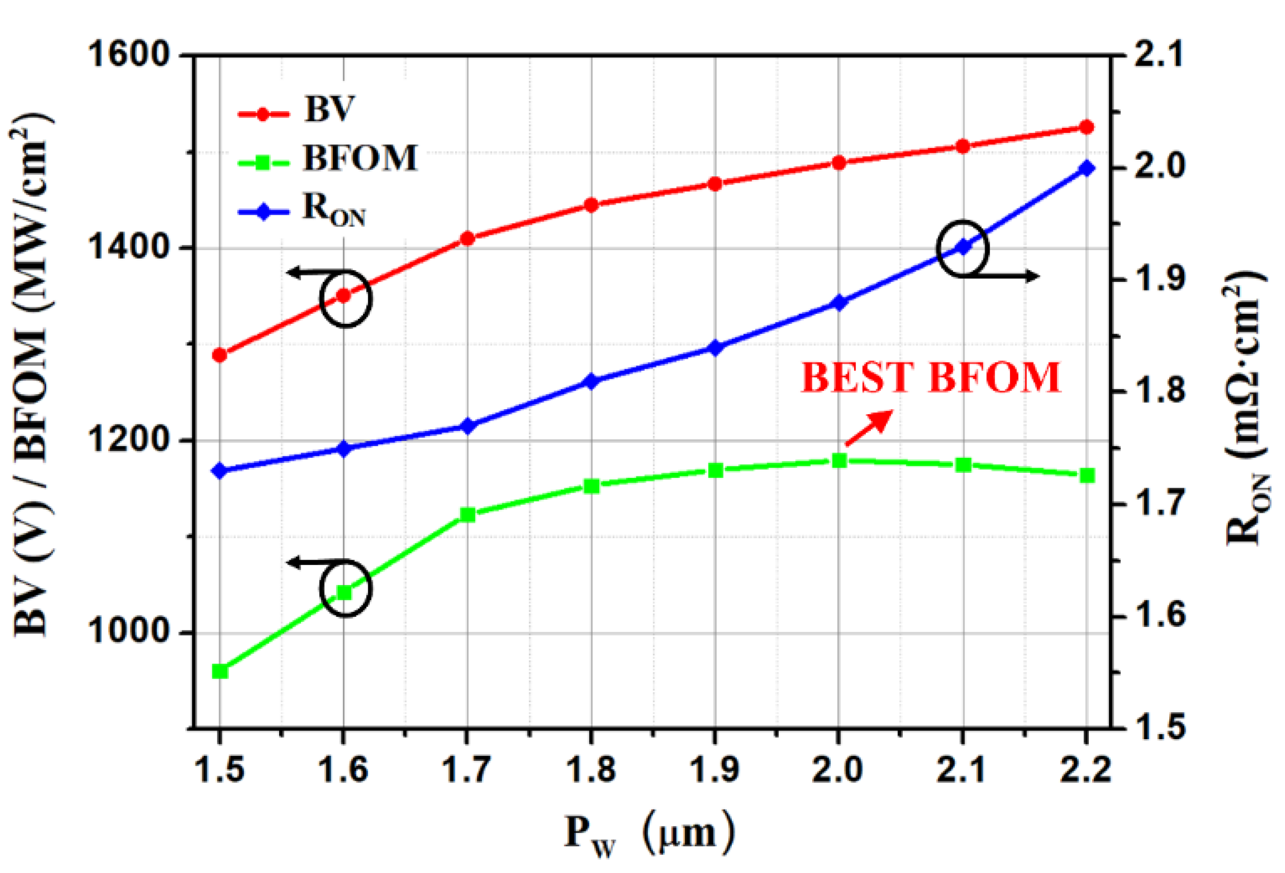
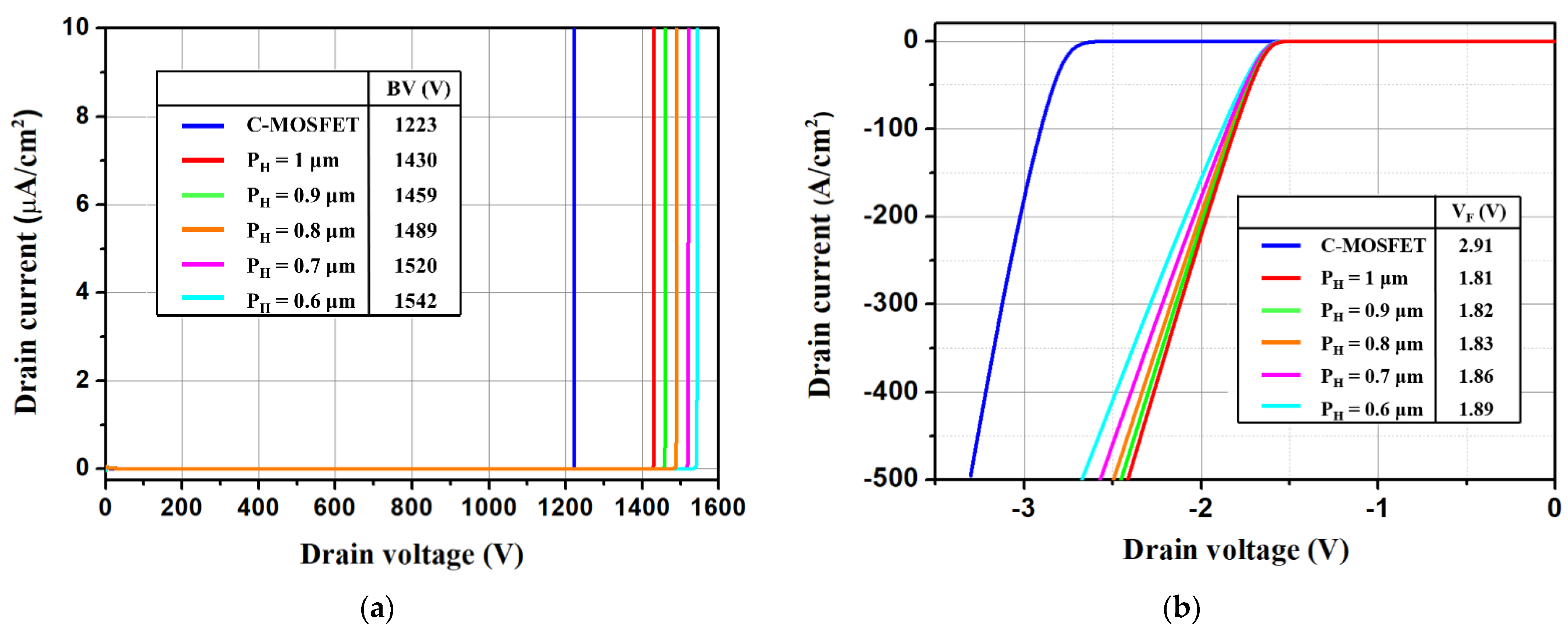
3.2. Optimization of the IHP-MOSFET
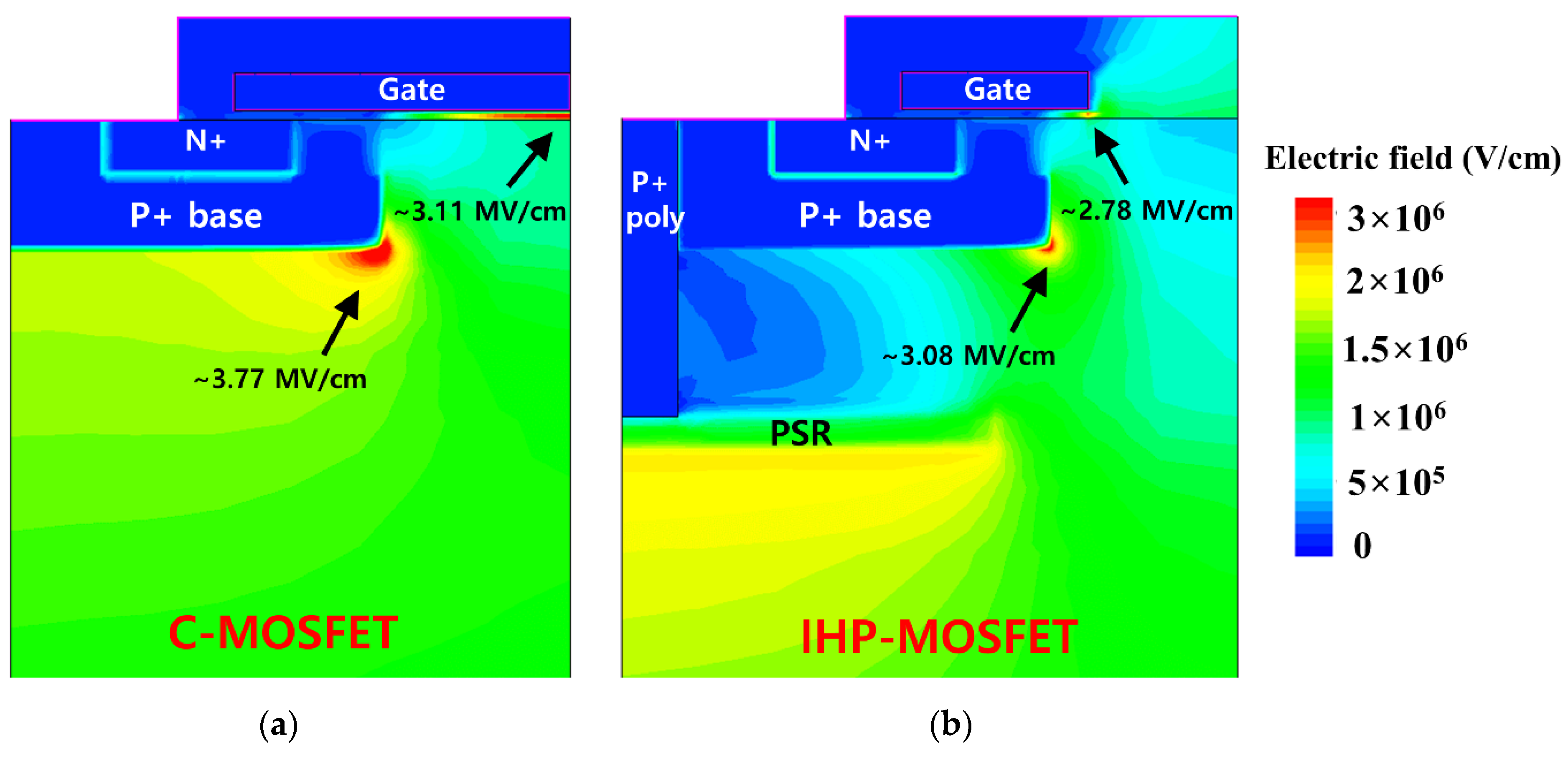
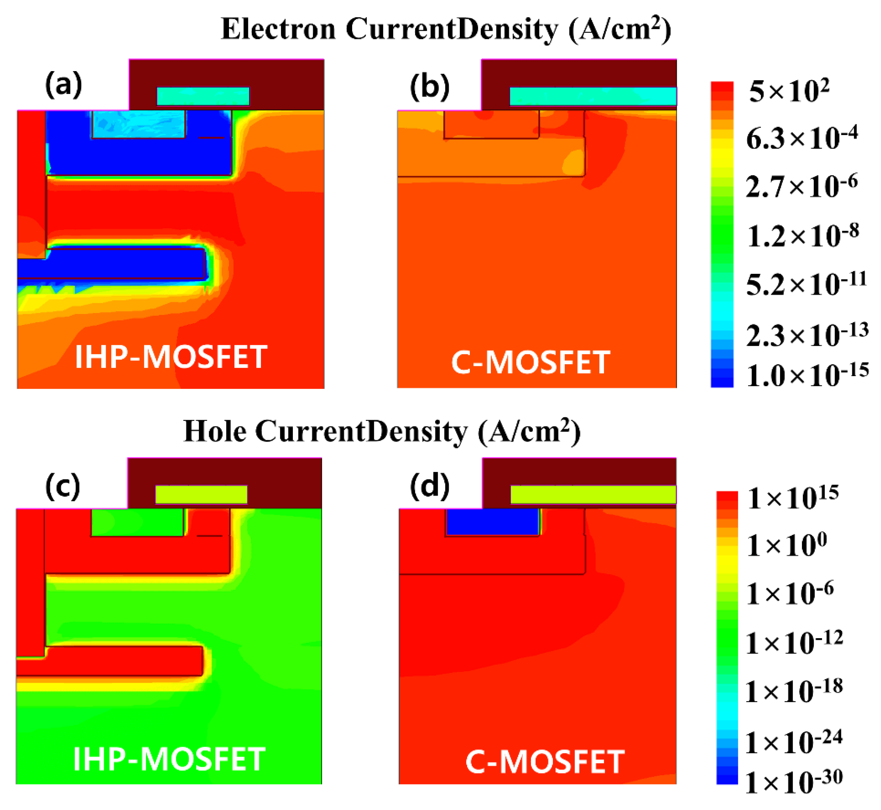
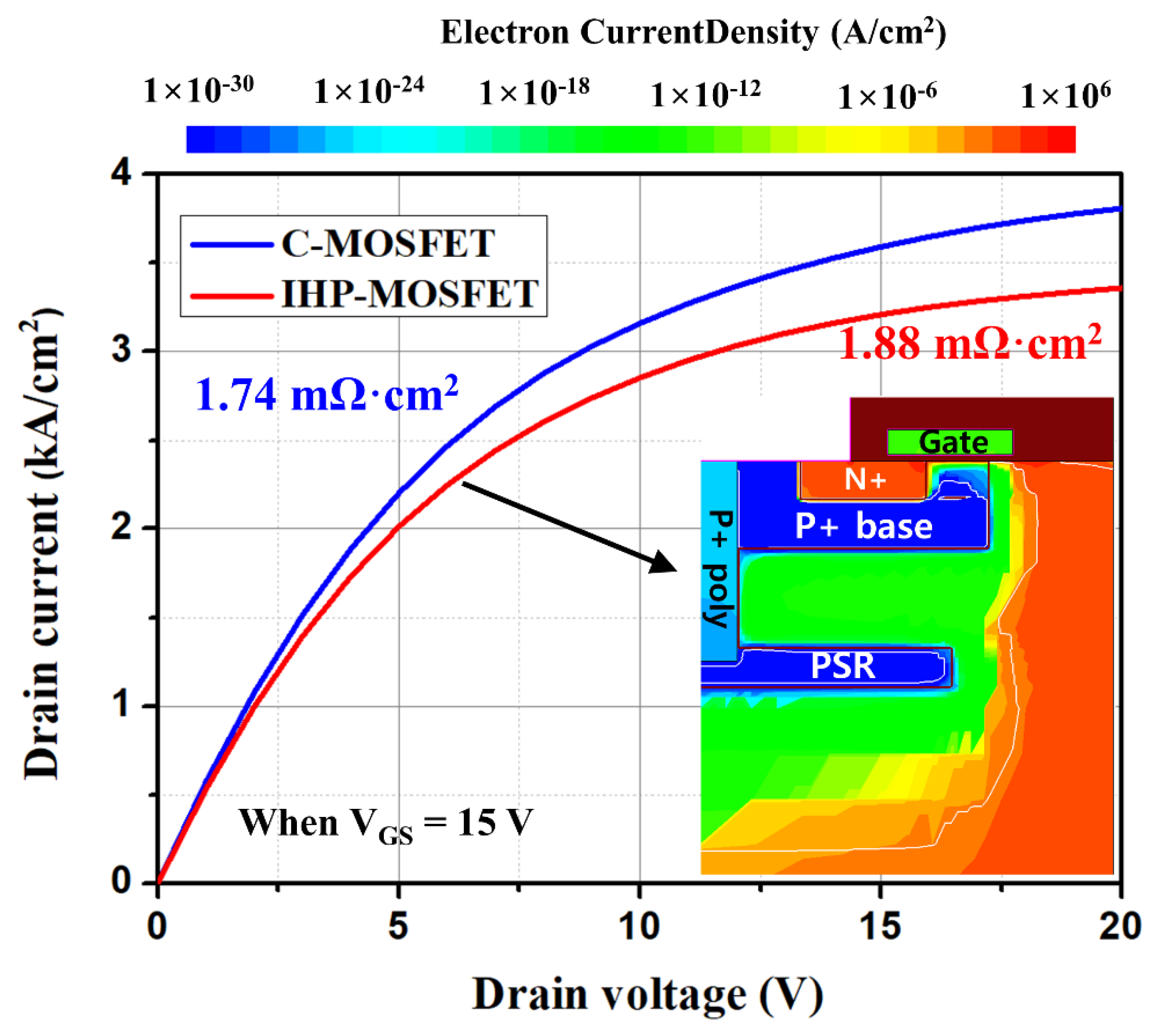
3.3. Device Performance Comparison of Both Devices
4. Conclusions
Author Contributions
Funding
Institutional Review Board Statement
Informed Consent Statement
Data Availability Statement
Acknowledgments
Conflicts of Interest
References
- Kimoto, T.; Cooper, J.A. Fundamentals of Silicon Carbide Technology: Growth Characterization Devices and Applications; Wiley: Singapore, 2014. [Google Scholar]
- Dong, L.; Sun, G.; Yu, J.; Zheng, L.; Liu, X.; Zhang, F.; Yan, G.; Li, X.; Wang, Z. Growth of 4H-SiC epilayers with low surface roughness and morphological defects density on 4 degrees off-axis substrates. Appl. Surf. Sci. 2013, 270, 301–306. [Google Scholar] [CrossRef]
- Shen, Z.; Zhang, F.; Dimitrijev, S.; Han, J.S.; Tian, L.X.; Yan, G.G.; Wen, Z.X.; Zhao, W.S.; Wang, L.; Liu, X.F.; et al. Prediction of High-Density and High-Mobility Two-Dimensional Electron Gas at AlxGa1-xN/4H-SiC Interface. Mate. Sci. Forum 2017, 897, 719–722. [Google Scholar] [CrossRef]
- Liu, G.; Ahyi, A.C.; Xu, Y.; Isaacs-Smith, T.; Sharma, Y.K.; Williams, J.R.; Feldman, L.C.; Dhar, S. Enhanced Inversion Mobility on 4H-SiC (112-0) Using Phosphorus and Nitrogen Interface Passivation. IEEE Electron Device Lett. 2013, 34, 181–183. [Google Scholar] [CrossRef]
- Cooper, J.J.A.; Melloch, M.R.; Singh, R.; Agarwal, A.; Palmour, J.W. Status and prospects for SiC power MOSFETs. IEEE Trans. Electron Devices 2002, 49, 658–664. [Google Scholar] [CrossRef]
- Godignon, P.; Soler, V.; Cabello, M.; Montserrat, J.; Rebollo, J.; Knoll, L.; Bianda, E.; Mihaila, A. New Trends in High Voltage MOSFET Based on Wide Band Gap Materials. In Proceedings of the International Semiconductor Conference (CAS), Sinaia, Romania, 11–14 October 2017. [Google Scholar]
- Sakai, T.; Murakami, N. A new VDMOSFET structure with reduced reverse transfer capacitance. IEEE Trans. Electron Devices 1989, 36, 1381–1386. [Google Scholar] [CrossRef]
- Han, K.J.; Baliga, B.J.; Sung, W.J. 1.2 kV 4H-SiC split-gate power MOSFET: Analysis and experimental results. Mater. Sci. Forum 2018, 924, 684–688. [Google Scholar] [CrossRef]
- Cha, K.; Yoon, J.; Kim, K. 3.3-kV 4H-SiC Split-Gate DMOSFET with Floating p+ Polysilicon for High-Frequency Applications. Electronics 2021, 10, 659. [Google Scholar] [CrossRef]
- Ishigaki, T.; Tatsunori, M.; Kinoshita, K.; Morikawa, T.; Oda, T.; Fujita, R.; Konishi, K.; Mori, Y.; Shima, A. Analysis of Degradation Phenomena in Bipolar Degradation Screening Process for SiC-MOSFETs. In Proceedings of the 31st International Symposium on Power Semiconductor Devices and ICs (ISPSD), Shanghai, China, 19–23 May 2019. [Google Scholar]
- An, J.; Hu, S. Heterojunction Diode Shielded SiC Split-Gate Trench MOSFET with Optimized Reverse Recovery Characteristic and Low Switching Loss. IEEE Access 2019, 7, 28592–28596. [Google Scholar] [CrossRef]
- Wang, Y.; Ma, Y.; Hao, Y.; Hu, Y.; Wang, G.; Cao, F. Simulation Study of 4H-SiC UMOSFET Structure With p+-polySi/SiC Shielded Region. IEEE Trans. Electron Devices 2017, 64, 3719–3724. [Google Scholar] [CrossRef]
- Han, Z.; Bai, Y.; Chen, H.; Li, C.; Lu, J.; Yang, C.; Yao, Y.; Tian, X.; Tang, Y.; Song, G.; et al. A Novel 4H-SiC Trench MOSFET Integrated with Mesa-Sidewall SBD. IEEE Trans. Electron Devices 2021, 68, 192–196. [Google Scholar] [CrossRef]
- Tian, L.; Yang, F.; Shen, Z.; Zhang, F.; Liu, X.; Yan, G.; Zhao, W.; Wang, L.; Sun, G.; Wu, J.; et al. Low leakage current and high unipolar current density in a 4H-SiC trench gate MOSFET with integrated Schottky barrier diode. In Proceedings of the 17th China International Forum on Solid State Lighting & 2020 International Forum on Wide Bandgap Semiconductors China (SSLChina: IFWS), Shenzhen, China, 23–25 November 2020; pp. 58–62. [Google Scholar]
- Li, X.; Tong, X.; Huang, A.Q.; Tao, H.; Zhou, K.; Jiang, Y.; Jiang, J.; Deng, X.; She, X.; Zhang, B.; et al. SiC Trench MOSFET with Integrated Self-Assembled Three-Level Protection Schottky Barrier Diode. IEEE Trans. Electron Devices 2018, 65, 347–351. [Google Scholar] [CrossRef]
- Jang, S.; Kim, J.; Lee, H.; Kim, K. Improved on-state resistance with reliable reverse characteristics in 1.2kV 4H-SiC MOSFET by selective nitrogen implantation assisted current spreading layer. Jpn. J. Appl. Phys. 2020, 59, 046501. [Google Scholar] [CrossRef]
- Wei, J.; Zhang, M.; Jiang, H.; To, X.; Kim, S.; Kim, J.; Chen, K.J. SiC trench IGBT with diode-clamped p-shield for oxide protection and enhanced conductivity modulation. In Proceedings of the IEEE 30th International Symposium on Power Semiconductor Devices and ICs (ISPSD), Chicago, IL, USA, 13–17 May 2018; pp. 411–414. [Google Scholar]
- Wei, J.; Zhang, M.; Jiang, H.; Wang, H.; Chen, K.J. Dynamic Degradation in SiC Trench MOSFET With a Floating p-Shield Revealed with Numerical Simulations. IEEE Trans. Electron Devices 2017, 64, 2592–2598. [Google Scholar] [CrossRef]
- Han, Z.; Song, G.; Bai, Y.; Chen, H.; Liu, X.; Lu, J. A novel 4H-SiC MOSFET for low switching loss and high reliability applications. Semicond. Sci. Technol. 2020, 35, 085017. [Google Scholar] [CrossRef]
- Jiang, J.-Y.; Wu, T.-L.; Zhao, F.; Huang, C.-F. Numerical Study of 4H-SiC UMOSFETs with Split-Gate and P+ Shielding. Energies 2020, 13, 1122. [Google Scholar] [CrossRef] [Green Version]
- Kim, J.; Kim, K. 4H-SiC Double-Trench MOSFET with Side Wall Heterojunction Diode for Enhanced Reverse Recovery Performance. Energies 2020, 13, 4602. [Google Scholar] [CrossRef]
- Na, J.; Cheon, J.; Kim, K. 4H-SiC Double Trench MOSFET with Split Heterojunction Gate for Improving Switching Characteristics. Materials 2021, 14, 3554. [Google Scholar] [CrossRef] [PubMed]
- Kobayashi, Y.; Harada, S.; Ishimori, H.; Takasu, S.; Kojima, T.; Ariyoshi, K.; Sometani, M.; Senzaki, J.; Takei, M.; Tanaka, Y.; et al. 3.3kV-Class 4H-SiC UMOSFET by Double Trench with Tilt Angle Ion implantation. Mater. Sci. Forum 2016, 858, 974–977. [Google Scholar] [CrossRef]
- Yoon, J.; Kim, K. A Novel MOS-Channel Diode Embedded in a SiC Superjunction MOSFET for Enhanced Switching Performance and Superior Short Circuit Ruggedness. Electronics 2021, 10, 2619. [Google Scholar] [CrossRef]
- TCAD Sentaurus Device Manual User Manual; Synopsys Inc.: Mountain View, CA, USA, 2015.
- Han, Z.; Bai, Y.; Chen, H.; Li, C.; Lu, J.; Song, G.; Liu, X. A trench/planar SiC MOSFET integrated with SBD (TPSBD) for low reverse recovery charge and low switching loss. Semicond. Sci. Technol. 2020, 35, 1–10. [Google Scholar] [CrossRef]
- Sasada, Y.; Kurumi, T.; Shimizu, H.; Kinoshita, H.; Yoshimoto, M. Junction formation via direct bonding of Si and 6H-SiC. Mater. Sci. Forum 2014, 778, 714–717. [Google Scholar] [CrossRef]
- Krishnaswami, S.; Das, M.; Hull, B.; Ryu, S.H.; Scofield, J.; Agarwal, A.; Palmour, J. Gate oxide reliability of 4H-SiC MOS devices. In Proceedings of the 43rd Annual, 2005 International Reliability Physics Symposium on IEEE, San Jose, CA, USA, 17–21 April 2005. [Google Scholar]
- Vudumula, P.; Kotamraju, S. Design and Optimization of 1.2-kV SiC Planar Inversion MOSFET Using Split Dummy Gate Concept for High-Frequency Applications. IEEE Trans. Electron Devices 2019, 66, 5266–5271. [Google Scholar] [CrossRef]


| Parameter | C-MOSFET | IHP-MOSFET | Unit |
|---|---|---|---|
| Epi-layer thickness | 10 | 10 | μm |
| N-drift doping | 8 × 10¹⁵ | 8 × 10¹⁵ | cm−3 |
| CSL doping | 4 × 10¹⁶ | 4 × 10¹⁶ | cm−3 |
| Length of the channel | 0.5 | 0.5 | μm |
| Channel doping | 2 × 10¹⁷ | 2 × 10¹⁷ | cm−3 |
| P+ base doping | 5 × 10¹⁸ | 5 × 10¹⁸ | cm−3 |
| N+ source doping | 1 × 10¹⁹ | 1 × 10¹⁹ | cm−3 |
| PSR doping | - | 5 × 10¹⁷ | cm−3 |
| Width of P+ base | 2 | 2 | μm |
| Half-cell pitch | 3 | 3.3 | μm |
| Width of JFET | 1 | 1 | μm |
| Oxide thickness (tox) | 50 | 50 | nm |
| Width of P+ polysilicon | - | 0.3 | μm |
| Width of PSR (PW) | - | 2 | μm |
| Distance between P+ base and PSR (PH) | - | 0.8 | μm |
| N+ substrate doping | 1 × 10¹⁹ | 1 × 10¹⁹ | cm−3 |
| N+ substrate thickness | 100 | 100 | μm |
| C-MOSFET | IHP-MOSFET | Unit | |
|---|---|---|---|
| VF 1 | 2.91 | 1.83 | V |
| BV 2 | 1223 | 1489 | V |
| RON 3 | 1.74 | 1.88 | mΩ·cm2 |
| BFOM (= BV2/RON) | 860 | 1179 | MW/cm2 |
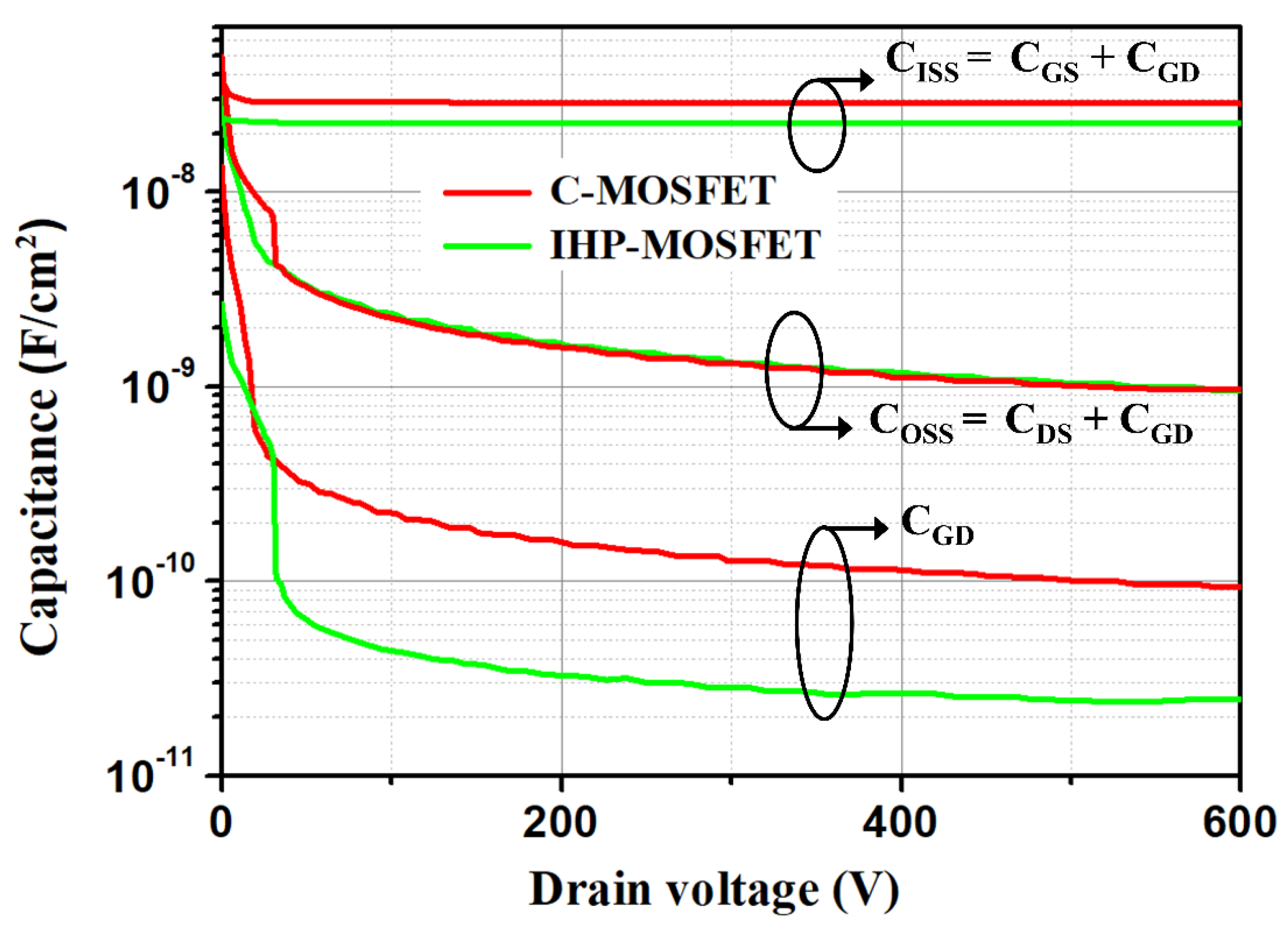
| CISS 4 | 28.48 | 22.51 | nF/cm2 |
| CGD 4 | 93.25 | 23.89 | pF/cm2 |
| COSS 4 | 951.89 | 962.42 | pF/cm2 |
| HFFOM (= RON × CGD) | 162.26 | 44.91 | mΩ∙pF |
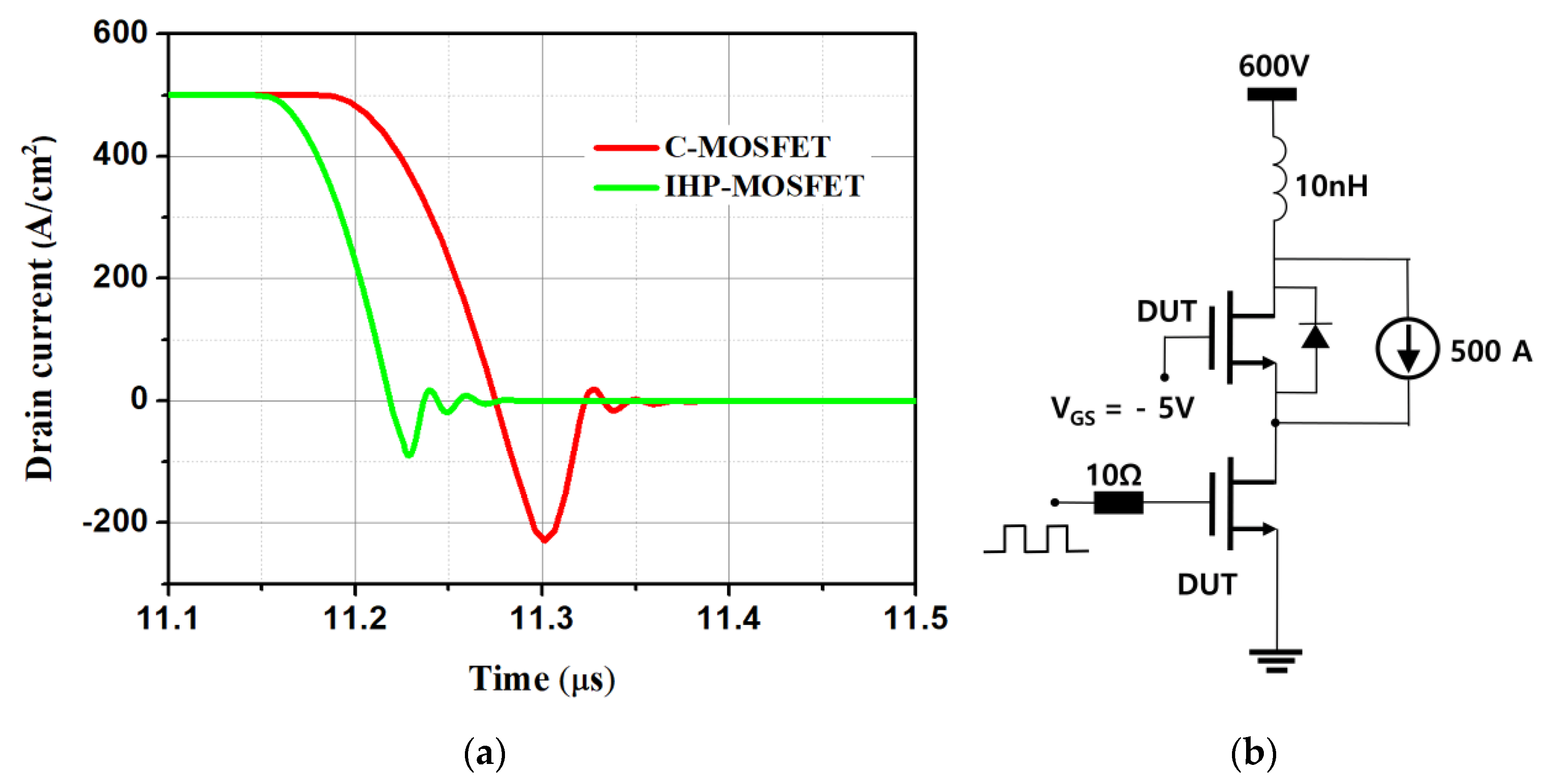
| IRRM | 230 | 90 | A/cm2 |
| trr | 48 | 18 | ns |
| Qrr | 6220 | 890 | nC/cm2 |
| C-MOSFET | IHP-MOSFET | Unit | |
|---|---|---|---|
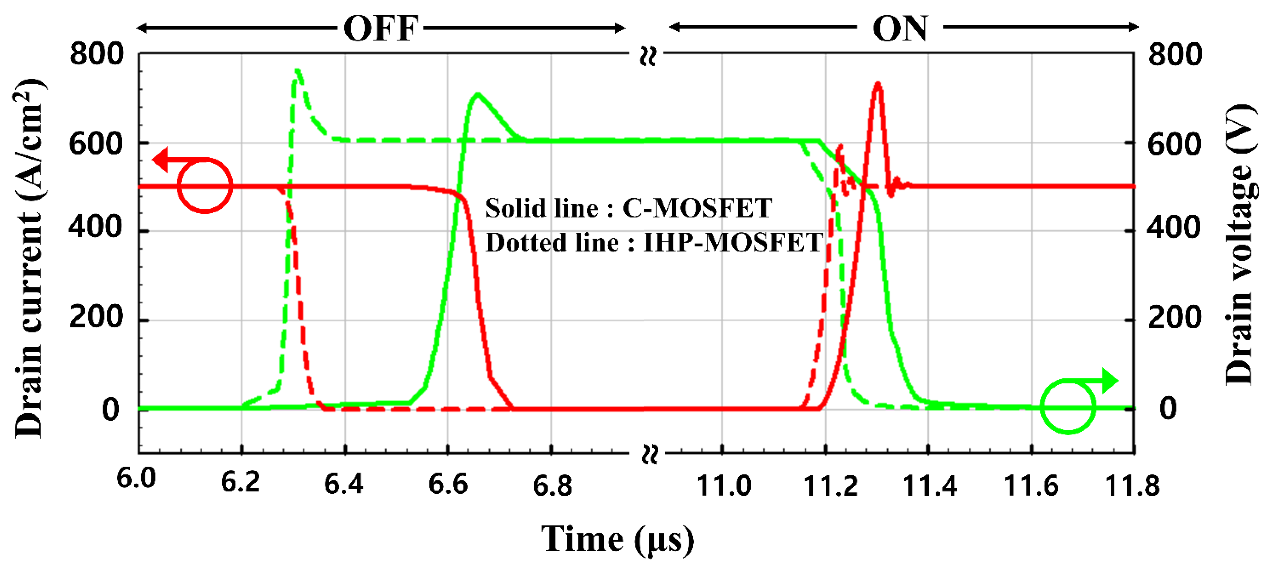
| TOFF | 544 | 244 | ns |
| TON | 303 | 197 | ns |
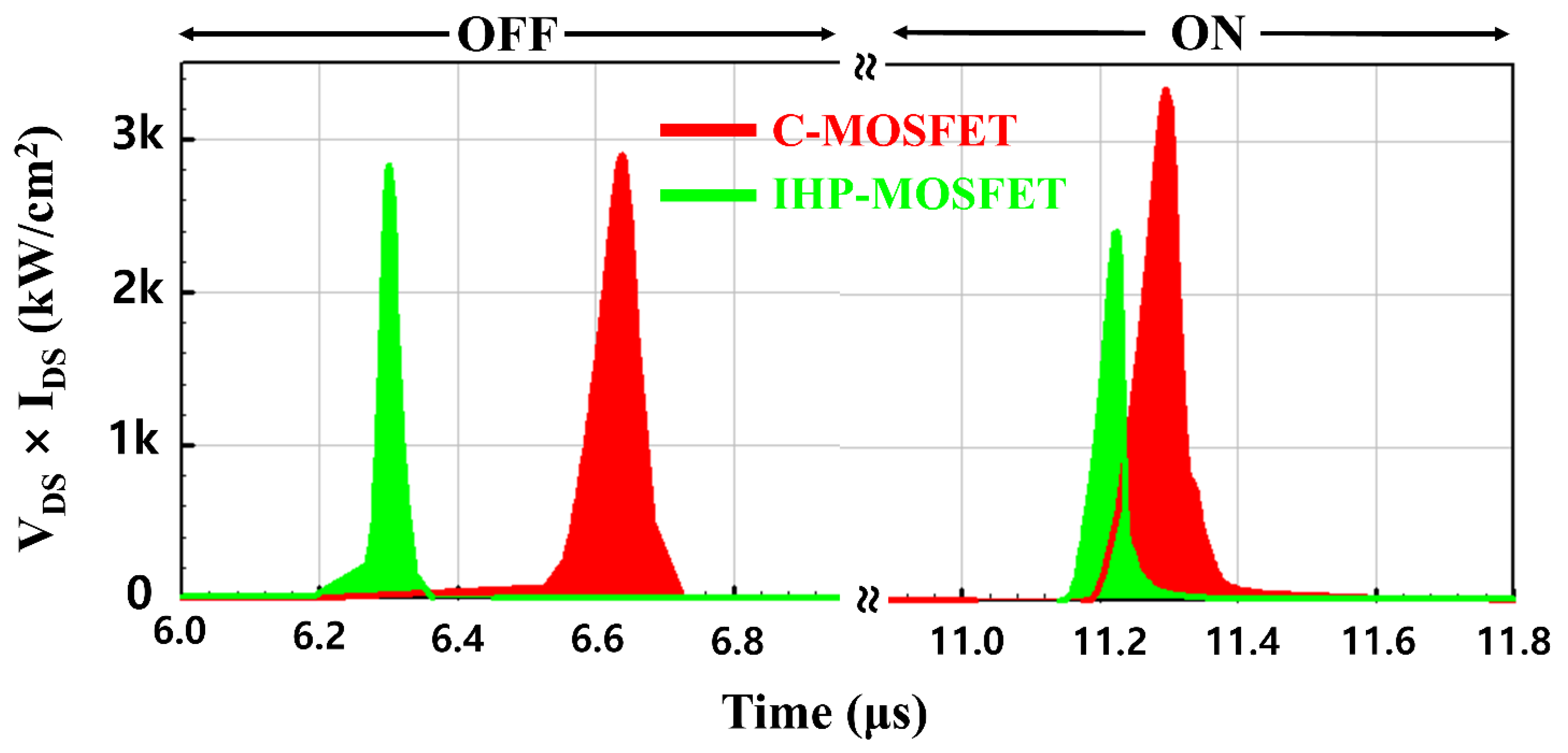
| EOFF | 10.70 | 3.70 | mJ/cm2 |
| EON | 23.25 | 10.05 | mJ/cm2 |
| ESW (= EON + EOFF) | 33.95 | 13.75 | mJ/cm2 |
Publisher’s Note: MDPI stays neutral with regard to jurisdictional claims in published maps and institutional affiliations. |
© 2021 by the authors. Licensee MDPI, Basel, Switzerland. This article is an open access article distributed under the terms and conditions of the Creative Commons Attribution (CC BY) license (https://creativecommons.org/licenses/by/4.0/).
Share and Cite
Yoon, J.; Na, J.; Kim, K. A 1.2 kV SiC MOSFET with Integrated Heterojunction Diode and P-shield Region. Energies 2021, 14, 8582. https://doi.org/10.3390/en14248582
Yoon J, Na J, Kim K. A 1.2 kV SiC MOSFET with Integrated Heterojunction Diode and P-shield Region. Energies. 2021; 14(24):8582. https://doi.org/10.3390/en14248582
Chicago/Turabian StyleYoon, Jongwoon, Jaeyeop Na, and Kwangsoo Kim. 2021. "A 1.2 kV SiC MOSFET with Integrated Heterojunction Diode and P-shield Region" Energies 14, no. 24: 8582. https://doi.org/10.3390/en14248582