Article

Asymmetric Split-Gate 4H-SiC MOSFET with Embedded Schottky Barrier Diode for High-Frequency Applications

Department of Electronic Engineering, Sogang University, Seoul 04107, Korea
*
Author to whom correspondence should be addressed.
Energies 2021, 14(21), 7305; https://doi.org/10.3390/en14217305
Submission received: 5 October 2021 / Revised: 29 October 2021 / Accepted: 2 November 2021 / Published: 4 November 2021
(This article belongs to the Special Issue Advances in Power Electronics Technologies)

Abstract

:
4H-SiC Metal-Oxide-Semiconductor Field Effect Transistors (MOSFETs) with embedded Schottky barrier diodes are widely known to improve switching energy loss by reducing reverse recovery characteristics. However, it weakens the static characteristics such as specific on-resistance and breakdown voltage. To solve this problem, in this paper, an Asymmetric 4H-SiC Split Gate MOSFET with embedded Schottky barrier diode (ASG-MOSFET) is proposed and analyzed by conducting a numerical TCAD simulation. Due to the asymmetric structure of ASG-MOSFET, it has a relatively narrow junction field-effect transistor width. Therefore, despite using the split gate structure, it effectively protects the gate oxide by dispersing the high drain voltage. The Schottky barrier diode (SBD) is also embedded next to the gate and above the Junction Field Effect transistor (JFET) region. Accordingly, since the SBD and the MOSFET share a current path, the embedded SBD does not increase in RON,SP of MOSFET. Therefore, ASG-MOSFET improves both static and switching characteristics at the same time. As a result, compared to the conventional 4H-SiC MOSFET with embedded SBD, Baliga′s Figure of Merit is improved by 17%, and the total energy loss is reduced by 30.5%, respectively.

1. Introduction

4H-SiC is a wide bandgap material and has material properties such as high critical electric field and thermal conductivity [1]. With these characteristics, the use of 4H-SiC enables the implementation of MOSFETs, which significantly improves the switching characteristics compared to the conventional Si IGBT [2,3]. Therefore, 4H-SiC Metal-Oxide-Semiconductor Field Effect Transistors (MOSFETs) are considered to be promising candidates for high-voltage and high-frequency applications. In particular, high-voltage and high-frequency power devices are expected to be applied in applications requiring high-power density, such as high-power converters and traction drives [4,5]. However, most commercially available SiC power MOSFETs are for 1200 V and 1700 V applications. In response to these industry demands, SiC MOSFETs for 3300 V are being actively researched [6,7]. Recently, various studies into trench MOSFETs have been conducted due to the high channel mobility and the small cell pitch of trench MOSFETs. However, trench MOSFETs suffer from electric field concentrations at the trench gate oxide corners exceeding 3 MV/cm, the gate oxide reliability limit of SiC MOSFETs [8]. Therefore, for high voltage applications, research mainly focuses on planar MOSFETs.
To achieve fast switching speeds and low switching energy losses for high frequency, the gate—drain capacitance (CGD) must be minimized [9]. A well-known method to reduce CGD of the planar MOSFET is a split gate MOSFET, which reduces the overlapped region between gate and drain through the split active gate [10]. However, in this structure, the electric field is concentrated at the corner of the split gate oxide, so there is a problem in that the reliability of the gate oxide cannot be guaranteed. In particular, this problem becomes more serious as the high-voltage device increases. Therefore, the split gate structure is difficult to apply to high voltage applications (>3.3 kV).
Another way to improve the switching characteristic is to improve the reverse recovery characteristics. Because the body diode of SiC MOSFETs has a high reverse recovery charge, a high reverse recovery current is generated during the turn on transient in the switching operation [11]. The reverse recovery current increases the peak drain current, resulting in high switching energy loss. To handle the reverse recovery current, an external Schottky barrier diode (SBD) is widely used as a freewheeling diode to suppress the action of the body diode [12]. However, an external SBD increases the active chip area and package cost. In high voltage applications, the active chip area of external SBD increases as the size of the external SBD increases to withstand the high voltage in the off state [13]. Recently, to improve the reverse recovery characteristics of SiC MOSFETs without using an external SBD, research into embedding SBD in SiC MOSFET has been actively conducted. A conventional 4H-SiC MOSFET with embedded SBD (C-MOSFET) greatly improves reverse recovery characteristics without external SBD [14]. However, embedded SBD increases the cell pitch, decreasing the channel density and thus increases the specific on-resistance (RON,SP). Moreover, in the off state, due to the increased mesa region, the voltage concentrated on the p+ base is also increased, reducing the Breakdown Voltage (BV). That is, the SBD embedded in the mesa region improves the reverse recovery characteristic but is accompanied by a deterioration of the static characteristics.
In this paper, we propose an asymmetric split gate 4H-SiC MOSFET with embedded SBD (ASG-MOSFET) to simultaneously improve both the switching and static characteristics. In ASG-MOSFET, the SBD is embedded next to the active gate and above the junction field effect transistor (JFET) region. Accordingly, the embedded SBD does not degrade the RON,SP of MOSFET because the MOSFET and SBD share the current path in the on state. In addition, since the ASG-MOSFET is an asymmetric structure, it has a narrow JFET width (WJFET). Therefore, it has a high channel density through a small cell pitch, thus reducing the RON,SP despite the narrow WJFET. This narrow WJFET also forms a large depletion region, creating a small depletion capacitance (CDEP). Moreover, the split gate structure of ASG-MOSFET reduces the overlapping area between gate and drain, thereby reducing gate oxide capacitance (COX). Therefore, ASG-MOSFET significantly reduces CGD through the reduced COX and CDEP.
This study was conducted by a Sentaurus TCAD simulation tool. In this simulation, the used models include the Fermi–Dirac statistics, band narrowing, anisotropic material properties, Shockley-Read-Hall, Auger recombination. A Hatakeyama model is used to consider the impact of ionization behavior. Mobility models, such as doping dependent, high field saturation, surface roughness, and acoustic phonon scattering at the SiC/SiO2 interface are involved [15]. The incomplete ionization model is also considered and the nonlocal tunneling model and Schottky barrier lowering model are used for the tunneling current at the Schottky contact [16]. The fixed charge concentration at the SiC/SiO2 interface is considered as 3 × 1012 cm−2.

2. Device Structure and Optimization

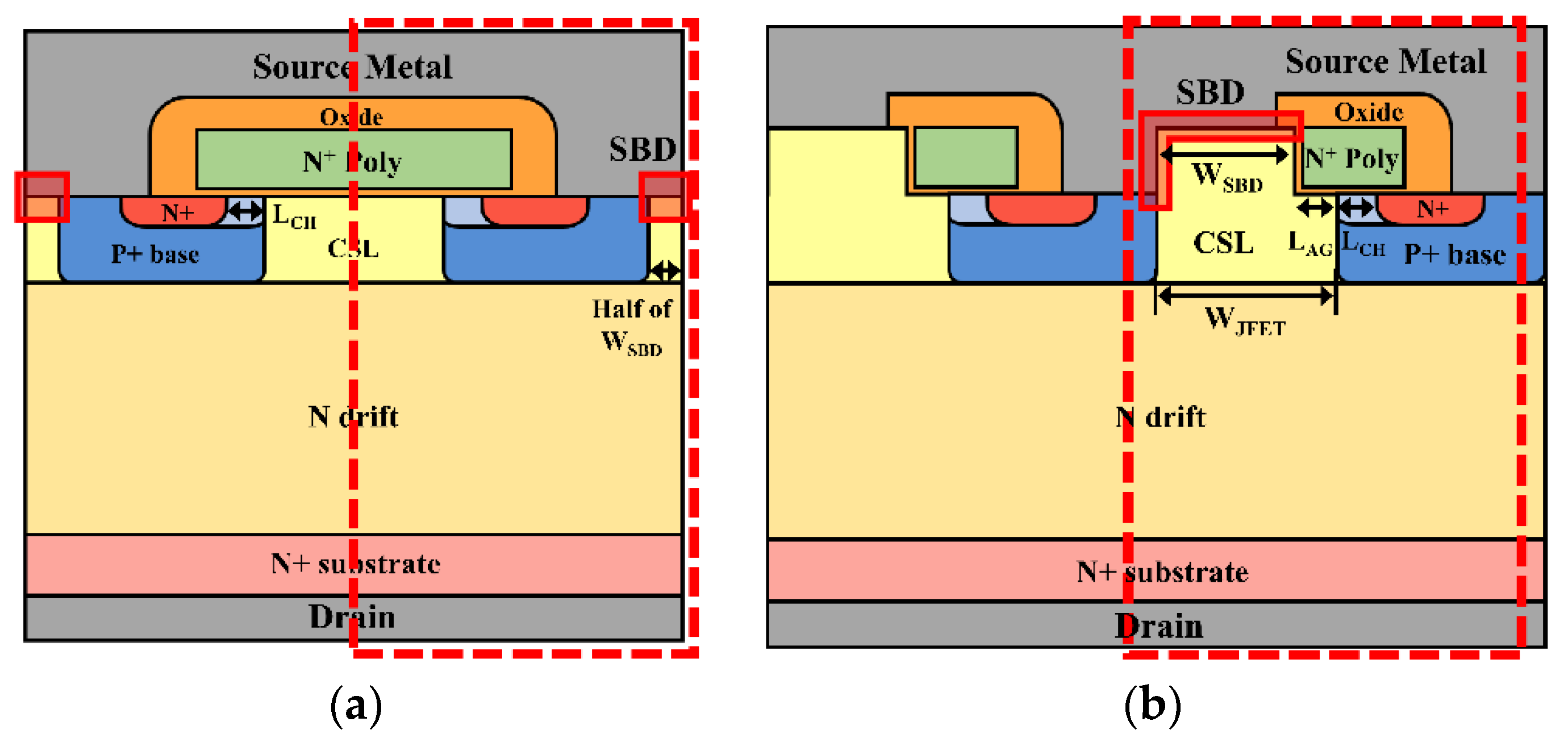
2.1. Proposed Device Structure

Figure 1 is a cross-sectional view of the C-MOSFET and the proposed ASG-MOSFET. In Figure 1, the cells used for the simulation are marked with a red dotted line. In Figure 1, the C-MOSFET and the ASG-MOSFET have the SBD embedded over the mesa region and the JFET region, respectively.
For the two device structures, the channel length and gate oxide thicknesses are 0.5 μm and 50 nm, respectively, and the doping concentration in the channel region is 2 × 1017 cm−3. Considering the simultaneous formation of ohmic and Schottky contacts using Ni as a source metal, the work function of the Schottky metal was set to 5.05 eV [17]. The electron mobility is set at about 20–50 cm2V−1S−1 in the 15 nm range below the SiC/SiO2 interface. A P+ base region doping concentration of 2 × 1018 cm−3, an N-drift layer of 30 μm, an N-drift doping concentration of 3 × 1015 cm−3, and a Channel Spread Layer (CSL) doping concentration of 2 × 1016 cm−3 were used. A heavily doped 1 × 1020 cm−3 N-type Poly Si was adopted as the active gate. The WJFET of C-MOSFET was set to 2.0 μm in consideration of static characteristics such as RON,SP, and BV. The gate oxide thickness of the two structures was considered to be 50 nm.

2.2. Key Parameter Optimization

In this section, optimization of the two structures was performed considering RON,SP and turn on voltage of embedded SBD (VF,SBD) of C-MOSFET and ASG-MOSFET. As previously mentioned, the C-MOSFET improves the reverse recovery characteristic through the embedded SBD, but it accompanies the degradation of the static characteristic. Therefore, the SBD width (WSBD) of C-MOSFET was designed considering RON,SP and VF,SBD. Figure 2 shows RON,SP and VF,SBD according to WSBD change in C-MOSFET. As WSBD increases, VF,SBD decreases while RON,SP increases. This is because the embedded SBD in the mesa region increases the cell pitch of the C-MOSFET, reducing the channel density. Therefore, considering both RON,SP and VF,SBD, 2.0 μm with the most appropriate performance was determined as the WSBD.
For a fair comparison between C-MOSFET and ASG-MOSFET, the WJFET of ASG-MOSFET is designed such that the BV of the ASG-MOSFET has a BV similar to that of the C-MOSFET. In the ASG-MOSFET, the WJFET consists of WSBD, the active gate length (LAG) and the gate oxide thickness (TOX). The LAG and TOX of ASG-MOSFET is fixed to 0.2 μm and 50nm. Therefore, the WJFET of the ASG-MOSFET was optimized by adjusting the WSBD.
Figure 3 shows the effect of WJFET on static characteristics of the ASG-MOSFET. In Figure 3a, unlike C-MOSFET, when WSBD increases, VF,SBD and RON,SP decrease simultaneously. In other words, the embedded SBD of the ASG-MOSFET does not degrade the RON,SP characteristic of the ASG-MOSFET. This is because the MOSFET channel and the embedded SBD share a current path through the JFET region in their respective on state. Meanwhile, from Figure 3b, in the off state, as the WJFET increases, the BV decreases due to the reduction of the screening effect by the JFET region. As a result, 1.4 μm, the condition with the most similar BV to that of C-MOSFET, was determined as WJFET. Therefore, WSBD, LAG, and TOX of the optimized ASG-MOSFET were designed to be 1.4 μm, 0.2 μm, and 50 nm, respectively.

3. Electrical Characteristics Analysis

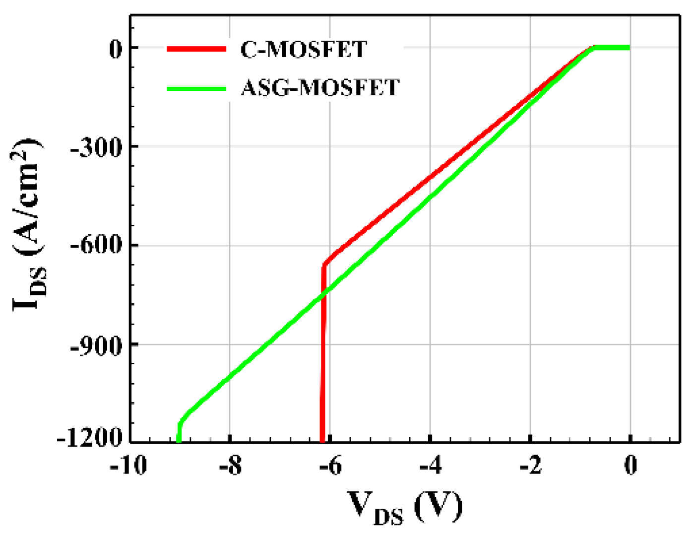
3.1. Static Characteristics

In this section, to verify the excellent electrical properties of the proposed ASG-MOSFET, the electrical properties of the two structures were compared and analyzed through TCAD simulation.
Figure 4 shows output curves and BV characteristics of the C-MOSFET and ASG-MOSFET. According to the results optimized in Section 2.2, C-MOSFET and ASG-MOSFET have similar BV of 4094 V and 4141 V, respectively. Whereas, The RON,SP of both structures are 10.12 mΩ·cm2 and 8.85 mΩ·cm2, respectively. ASG-MOSFET has higher JFET resistance than C-MOSFET due to smaller WJFET, but RON,SP of ASG-MOSFET is 12.5% smaller than C-MOSFET. This is because the ASG-MOSFET has a smaller cell pitch, which increases the channel density. As a result, the BFOM calculated by BV2/RON,SP improved by 17 %, respectively, compared to C-MOSFET.
The electric field distributions of C-MOSFET and ASG-MOSFET when VDS = 3000 V are plotted in Figure 5a,b, respectively. The C-MOSFET has the highest gate oxide electric field (EOX) in the center of the gate oxide because the WJFET is wide. On the other hand, in ASG-MOSFET, the split gate corner is most vulnerable to electric field. However, because the ASG-MOSFET has an asymmetric structure, the gate oxide is more effectively protected by forming a wide depletion region in the JFET region through a narrow WJFET. As a result, the maximum EOX of C-MOSFET and ASG-MOSFET is 2.74 MV/cm and 2.02 MV/cm, respectively, so ASG-MOSFET has a more superior gate oxide reliability.
Figure 6 shows the forward conduction characteristics of the body diode. The forward conduction characteristics were extracted by sweeping VDS from 0 V to −10 V when VGS = −5 V. In Figure 6, the VF,SBD is defined as the VDS when the drain current reaches −80 A/cm2. Meanwhile, the knee point means the point at which the body diode is turned on [18]. As a result, VF,SBD of C-MOSFET is 1.45 V, whereas VF,SBD of ASG-MOSFET is 1.35 V. Therefore, the ASG-MOSFET more effectively suppresses the turn on of the body diode. The static characteristics of the two devices, including RON,SP, BV, maximum EOX, VF,SBD and turn on voltage of body diode (VF,Body), are summarized in Table 1. In addition, Baliga′s Figure of Merit (BFOM), which is the static characteristic indicator considering RON,SP and BV, was calculated and listed.

3.2. Dynamic Characteristics

The capacitance simulation results of two devices are depicted in Figure 7. In the capacitance simulation, the capacitance was extracted by sweeping the drain voltage from 0 V to 1500 V when VGS = 0 V, and the AC small signal was set to 1 MHz. In addition, the active area of two devices of two devices is set to 1 cm2.
From Figure 7a, it can be seen that the input capacitance (CISS) and the output capacitance (COSS) of two structures are very similar. In the Figure 7b, the ASG-MOSFET has a significant improvement in CGD over C-MSOFET. The CGD of ASG-MOSFET is 6.04 pF/cm2, which is improved by 60.4% compared to 15.24 pF/cm2 of C-MOSFET. This is because the ASG-MOSFET greatly reduces the COX and CDEP constituting CGD. The CGD is a series connection of COX and CDEP [9]. The split-gate structure of ASG-MOSFET effectively reduces the overlapping area between gate and drain, reducing the COX. In addition, narrow WJFET of ASG-MOSFET forms a wide depletion region between gate and drain, which also reduces CDEP. Therefore, the ASG-MOSFET has significantly reduced CGD. Based on the RON,SP and CGD results, High-Frequency Figure of Merit (HFFOM), which is commonly used as the high frequency performance indicators is calculated [2]. As a result, owing to the reduced RON,SP and CGD, the HFFOM of the ASG-MOSFET is 53.45 mΩ·pF, which is a 65% improvement compared to the 154.23 mΩ·pF of the C-MOSFET.
Figure 8 shows the switching waveforms of both devices when used as a device under test (DUT) in a half-bridge circuit. Figure 8a shows this during the turn on transient and turn off transient, respectively, and Figure 8b appears to show the half bridge circuits used for the double pulse test simulation. In Figure 8b, the gate resistance is set to 10 Ω and the gate voltage switched from −5 V to 20 V. In order to proceed with the double pulse test of the 3.3 kV device, VDD was set to 1700 V. Furthermore, to set the load current to 100 A/cm2 in the test circuit, the time period of the first pulse and load inductance are set to 10 µs and 170 µH, respectively, considering the VDD and the rate of di/dt, and a parasitic inductance is assumed to 10 nH. In addition, the same MOSFET as the lower arm MOSFET was used for the upper arm MOSFET to handle the freewheeling current in the half-bridge circuit, and VGS of the upper arm MOSFET was applied to −5V to maintain the off state of the upper arm MOSFET. The SBD connected in parallel to the MOSFET in a half-bridge circuit appears in the SBD, which is embedded into the MOSFET.
In Figure 8a, the ASG-MOSFET has a shorter Miller plateau and a faster switching speed than C-MOSFET during the switching transients, which is consistent with the CGD results. Meanwhile, although SBD of ASG-MOSFET has lower VF,SBD than C-MOSFET, the peak current during switching transient is larger. This is because the fast-switching time of the ASG-MOSFET results in a higher overshoot current [19].
Figure 9 shows the current waveform of upper arm MOSFET during the turn on transient of lower arm MOSFET when the C-MOSFET and ASG-MOSFET are used as DUT in half-bridge circuit. From Figure 9, the ASG-MOSFET has a slightly larger reverse recovery charge (QRR) compared to the C-MOSFET. This is because the reduced CGD of the ASG-MOSFET causes a larger overshoot current, resulting in a higher peak current.
The ASG-MOSFET has a slightly larger QRR, but more superior the switching characteristics than the C-MOSFET. Figure 10 shows the total switching energy loss (ETotal) of two devices during the switching transient. The ETotal of the ASG-MOSFET is still lower than that of the C-MOSFET shown in Figure 10 due to its fast-switching speed. Based on the double pulse test simulation results, the turn off loss (EOFF) and the turn on loss (EON) of ASG-MOSFET are 0.84 mJ/cm2 and 3.19 mJ/cm2, respectively, whereas the C-MOSFET has an EOFF of 1.79 mJ/cm2 and an EON of 4.01 mJ/cm2, the ETotal of ASG-MOSFET is 4.03 mJ, which is 30.5% lower than that of C-MOSFET with ETotal of 5.80 mJ. As a result, the switching characteristics, including the parasitic capacitance and reverse recovery characteristics of the two devices, are summarized in Table 2.

4. Proposed Fabrication Process

Considering the feasibility of the proposed MOSFE, the fabrication process of ASG-MOSFET is proposed as shown in Figure 11. The N- drift and Channel Spread Layer are grown on an n+ substrate by epitaxial process, and the CSL layer is etched to remove the CSL layer, except for the Schottky contact region. N+ source, P+ base and P channel region are formed by the implantation process. The chemical vapor deposition is performed at 800 °C to form an oxide with a uniform thickness of 50 nm [20]. Poly Si is deposited by the low-pressure chemical vapor deposition (LPCVD) and is etched by reactive ion etching to form a split gate structure [21]. Interlayer dielectric oxide is deposited through LPCVD and is etched to open the Ohmic and Schottky contact region [22]. After Ni is deposited, rapid thermal annealing (RTA) is performed at 900 °C [23]. RTA at 900 °C after Ni deposition allows Ni to serve as a multifunctional metal that simultaneously forms Ohmic and Schottky contacts. Finally, an Ni layer is patterned, and a thick Al layer is deposited to form a metal pad.

5. Conclusions

In this paper, based on the TCAD simulation results, we propose and analyze an asymmetric 4H-SiC split-gate MOSFET with embedded SBD (ASG-MOSFET). ASG-MOSFET has narrower WJFET than C-MOSFET due to its asymmetric structure. The narrower WJFET forms a wide depletion region, causing a better shielding effect of the JFET region. Therefore, the split gate structure of ASG-MOSFET is effectively protected without degradation of BV and gate oxide reliability. ASG-MOSFET also has lower RON,SP than C-MOSFET. Unlike C-MOSFET, in ASG-MOSFET, the SBD is embedded above the JFET region so that the embedded SBD does not degrade the RON,SP and the ASG-MOSFET has a smaller cell pitch, increasing channel density. In addition, since narrow WJFET due to asymmetric structure effectively reduces CDEP, ASG-MOSFET effectively improves switching characteristics through split gate, narrow WJFET due to its asymmetric structure, and embedded SBD. As a result, ASG-MOSFET improved BFOM and switching energy loss by 17% and 30.5%, respectively, compared to C-MOSFET. Therefore, ASG-MOSFET is more suitable for high voltage and high frequency applications.

Author Contributions

All authors contributed to this work. Please confirm. Conceptualization, K.C.; methodology, K.C. and K.K.; software, K.C.; validation, K.C. and K.K.; formal analysis, K.C. and K.K.; investigation, K.C.; resources, K.C. and K.K.; writing—original draft preparation, K.C.; writing—review and editing, K.K.; visualization, K.C.; supervision, K.K.; project administration, K.C. and K.K.; All authors have read and agreed to the published version of the manuscript.

Funding

This research received no external funding.

Institutional Review Board Statement

Not applicable.

Informed Consent Statement

Not applicable.

Data Availability Statement

Data are not available on a publicly accessible repository and they cannot be shared under request.

Acknowledgments

This paper was supported by the MSIT (Ministry of Science and ICT), Korea, under the ITRC (Information Technology Research Center) support program (IITP-2021-2018-0-01421) supervised by the IITP (Institute for Information & communications Technology Promotion).

Conflicts of Interest

The authors declare no conflict of interest.

References

  1. Paul, T. Wide bandgap semiconductor power devices for energy efficient systems. In Proceedings of the 2015 IEEE 3rd Workshop on Wide Bandgap Power Devices and Applications (WiPDA), Blacksburg, VA, USA, 2–4 November 2015; pp. 402–405. [Google Scholar]
  2. Baliga, B.J. Fundamentals of Power Semiconductor Devices; Springer: New York, NY, USA, 2008. [Google Scholar]
  3. Godignon, P.; Soler, V.; Cabello, M.; Montserrat, J.; Rebollo, J.; Knoll, L.; Bianda, E.; Mihaila, A. New Trends in High Voltage MOSFET Based on Wide Band Gap Materials. In Proceedings of the International Semiconductor Conference (CAS), Sinaia, Romania, 11–14 October 2017. [Google Scholar]
  4. Zhang, M.; Wei, J.; Jiang, H.; Chen, K.J.; Cheng, C.H. Low ON-Resistance SiC Trench/Planar MOSFET With Reduced OFF-State Oxide Field and Low Gate Charges. IEEE Electron. Device Lett. 2016, 37, 1458–1461. [Google Scholar]
  5. Cooper, J.A.; Agarwal, A. SiC power-switching devices-the second electronics revolution? Proc. IEEE 2002, 90, 956–968. [Google Scholar] [CrossRef]
  6. Agarwal, A.; Baliga, B.J.; Francois, M.M.A.; Maxwell, E.; Berliner, N.; Papageorge, M. 3.3kV 4H-SiC Planar-Gate MOSFETs Manufactured using Gen-5 PRESiCE™ Technology in a 4-inch Wafer Commercial Foundry. In Proceedings of the SoutheastCon 2021, Atlanta, GA, USA, 10–13 March 2021; pp. 1–4. [Google Scholar]
  7. Baba, M.; Tawara, T.; Morimoto, T.; Harada, S.; Takei, M.; Kimura, H. Ultra-Low Specific on-Resistance Achieved in 3.3 kV-Class SiC Superjunction MOSFET 2021. In Proceedings of the 3rd International Symposium on Power Semiconductor Devices and ICs (ISPSD), Nagoya, Japan, 30 May–3 June 2021; pp. 83–86. [Google Scholar]
  8. Krishnaswami, S. Gate oxide reliability of 4H-SiC MOS devices. In Proceedings of the IEEE International Reliability Physics Symposium (IRPS), San Jose, CA, USA, 17–21 April 2005; pp. 592–593. [Google Scholar]
  9. Vudumula, P.; Kotamraju, S. Design and Optimization of 1.2-kV SiC Planar Inversion MOSFET Using Split Dummy Gate Concept for High-Frequency Applications. IEEE Electron. Device Lett. 2019, 66, 5266–5271. [Google Scholar] [CrossRef]
  10. Han, K.; Baliga, B.J.; Sung, W. Split-Gate 1.2-kV 4H-SiC MOSFET: Analysis and Experimental Validation. IEEE Electron. Device Lett. 2017, 38, 1437–1440. [Google Scholar] [CrossRef]
  11. Ishigaki, T.; Tatsunori, M.; Kinoshita, K.; Morikawa, T.; Oda, T.; Fujita, R.; Konishi, K.; Mori, Y.; Shima, A. 2019 Analysis of Degradation Phenomena in Bipolar Degradation Screening Process for SiC-MOSFETs. In Proceedings of the 31st International Symposium on Power Semiconductor Devices and ICs (ISPSD), Shanghai, China, 19–23 May 2019; pp. 259–262. [Google Scholar]
  12. Conrad, M.; De Doncker, R.W. Avoiding reverse recovery effects in super junction MOSFET based half-bridges. In Proceedings of the 2015 IEEE 6th International Symposium on Power Electronics for Distributed Generation Systems (PEDG), Aachen, Germany, 22–25 June 2015; pp. 1–5. [Google Scholar]
  13. Kawahara, K.; Hino, S.; Sadamatsu, K.; Nakao, Y.; Yamashiro, Y.; Yamamoto, Y.; Iwamatsu, T.; Tomohisa, S.; Yamakawa, S. 6.5 kV schottky-barrier-diode-embedded SiC-MOSFET for compact full-unipolar module. In Proceedings of the 2017 29th International Symposium on Power Semiconductor Devices and IC’s (ISPSD), Sapporo, Japan, 28 May–1 June 2017; pp. 41–44. [Google Scholar]
  14. Soltau, N.; Wiesner, E.; Hatori, K. Switching Performance of 750A/3300V Dual SiC-Modules. Bodo’s Power Syst. 2019, 2, 26–28. [Google Scholar]
  15. Han, Z.; Bai, Y.; Chen, H.; Li, C.; Lu, J.; Song, G.; Liu, X. A trench/planar sic mosfet integrated with SBD (TPSBD) for low reverse recovery charge and low switching loss. Semicond. Sci. Technol. 2020, 35, 1–10. [Google Scholar] [CrossRef]
  16. Synopsys, Inc. TCAD SentaurusTM Device User Guide; Synopsys, Inc.: Mountain View, CA, USA, 2017. [Google Scholar]
  17. Sung, W.; Baliga, B.J. On Developing One-Chip Integration of 1.2 kV SiC MOSFET and JBS Diode (JBSFET). IEEE Trans. Ind. Electron. 2017, 64, 8206–8212. [Google Scholar] [CrossRef]
  18. Pan, Y.; Tian, L.; Wu, H.; Li, Y.; Yang, F. 3.3kV 4H-SiC JBS diodes with single-zone JTE termination. Microelectron. Eng. 2017, 181, 10–15. [Google Scholar] [CrossRef]
  19. Shenai, K.; Baliga, B.J. Monolithically integrated power MOSFET and Schottky diode with improved reverse recovery characteristics. IEEE Trans. Electron. Devices 1990, 37, 1167–1169. [Google Scholar] [CrossRef]
  20. Ahn, J.; Ting, W.; Kwong, D.L. Comparison of performance and reliability between MOSFETs with LPCVD gate oxide and thermal gate oxide. IEEE Trans. Electron. Devices 1991, 38, 2709–2710. [Google Scholar] [CrossRef]
  21. Saxena, R.S.; Kumar, M.J. Dual-Material-Gate Technique for Enhanced Transconductance and Breakdown Voltage of Trench Power MOSFETs. IEEE Trans. Electron. Devices 2009, 56, 517–522. [Google Scholar] [CrossRef]
  22. Rao, V.R.; Eisele, I.; Patrikar, R.M.; Sharma, D.K.; Vasi, J.; Grabolla, T. High-field stressing of LPCVD gate oxides. IEEE Electron. Device Lett. 1997, 18, 84–86. [Google Scholar]
  23. Sung, W.; Baliga, B.J. Monolithically Integrated 4H-SiC MOSFET and JBS Diode (JBSFET) Using a Single Ohmic/Schottky Process Scheme Applications. IEEE Electron. Device Lett. 2016, 37, 1605–1608. [Google Scholar] [CrossRef]
Figure 1. Schematic cross-sectional views (a) conventional MOSFET with embedded SBD (C-MOSFET) and (b) asymmetric split gate MOSFET with embedded SBD (ASG-MOSFET).
Energies 14 07305 g001
Figure 2. Trade-off between RON,SP and VF,SBD of C-MOSFET according to WSBD.
Energies 14 07305 g002
Figure 3. Static characteristics of ASG-MOSFET according to WSBD (a) RON,SP and VF,SBD characteristics and (b) BV.
Energies 14 07305 g003
Figure 4. Output curve and BV characteristics of C-MOSFET and ASG-MOSFET.
Energies 14 07305 g004
Figure 5. Electric field distribution of (a) C-MOSFET and (b) ASG-MOSFET when VDS = 3000 V.
Energies 14 07305 g005
Figure 6. Forward conduction of the body diode of C−MOSFET and ASG−MOSFET.
Energies 14 07305 g006
Figure 7. Capacitance of C-MOSFET and ASG-MOSFET (a) Input and output capacitance and (b) Gate–drain capacitance.
Energies 14 07305 g007
Figure 8. (a) Switching waveforms of C-MOSFET and ASG-MOSFET during turn off transient and turn on transient and (b) half-bridge circuit used for double pulse test simulation.
Energies 14 07305 g008
Figure 9. Current waveform of upper arm MOSFET during the turn on transient of lower arm DUT.
Energies 14 07305 g009
Figure 10. Switching energy loss during turn off and turn on transients.
Energies 14 07305 g010
Figure 11. Proposed process flow of ASG-MOSFET. (a) Epitaxial N-drift layer and CSL on N+ substrate and Form the P+ base, P channel and N+ source by implantation (b) gate oxide deposition (c) Poly Si deposition and patterning (d) ILD deposition (e) ILD patterning (f) Ni metal deposition to form the ohmic and Schottky contact.
Energies 14 07305 g011
Table 1. Dynamic characteristics of two devices.
C-MOSFETASG-MOSFET
RON,SP (mΩ·cm2)10.128.85
BV (V)40984141
BFOM (MW/cm2)1659.51937.6
Maximum EOX (MV/cm)2.742.02
VF,SBD (V)1.451.35
VF,Body (V)6.129.0
Table 2. Dynamic characteristics of two devices.
C-MOSFETASG-MOSFET
CISS (nF/cm2)16.7917.34
COSS (pF/cm2)369.79369.71
CGD (pF/cm2)15.246.04
QRR (nC/cm2)1.181.26
EOFF (mJ/cm2)1.790.84
EON (mJ /cm2)4.013.19
ETotal (mJ/cm2)5.804.03
Publisher’s Note: MDPI stays neutral with regard to jurisdictional claims in published maps and institutional affiliations.

