Article

Optimizing Device Structure of PTB7-Th:PNDI-T10 Bulk Heterojunction Polymer Solar Cells by Enhancing Optical Absorption

by
Daniel Dodzi Yao Setsoafia
1,
Kiran Sreedhar Ram
1,
Hooman Mehdizadeh Rad
1,2,
David Ompong
1,2,
Naveen Kumar Elumalai
1 and
Jai Singh
1,2,*
1
College of Engineering, IT and Environment, Purple 12, Charles Darwin University, Darwin, NT 0909, Australia
2
Energy and Resources Institute, Charles Darwin University, Darwin, NT 0909, Australia
*
Author to whom correspondence should be addressed.
Energies 2022, 15(3), 711; https://doi.org/10.3390/en15030711
Submission received: 18 November 2021 / Revised: 4 January 2022 / Accepted: 7 January 2022 / Published: 19 January 2022
(This article belongs to the Special Issue Advances in Power Electronics Technologies)

Abstract

:
Using the optical transfer matrix method, we optimized the layered structure of a conventional and an inverted BHJ OSC with the active layer made of blended PTB7-Th:PNDI-T10 by maximizing the optical absorption and, hence, the J S C . The maximum J S C thus obtained from the optimised structure of the inverted OSC was 139 Am−2 and that of the conventional OSC was 135 Am−2. Simulation of the electric field distribution in both inverted and conventional OSCs showed that the formation of a single CIP was obtained in the active layer of thickness 105 nm in both OSCs. As the light incidents from the ITO side, it was found that excitons were generated more closely to ITO electrode, which favors the efficient charge transport and collection at the opposite electrodes in the inverted OSC, which produces higher J S C .

Graphical Abstract

1. Introduction

Increasing demand for clean energy and utilization of environmentally sustainable means for generating electricity are fueling the rapid development and commercialization of a broad range of renewable energy technologies [1,2,3,4]. The conversion of solar energy to electricity remains an indispensable part of the renewable energy portfolio due to the ubiquity of solar radiation, which is generated outside the planet Earth [5]. Such a conversion from solar energy to electricity is carried out by solar cells, which are semiconductor devices fabricated from both inorganic and organic semiconductors. However, the photovoltaic research is currently focused on the development of efficient organic solar cells (OSCs) as an alternative to the well-established inorganic counterparts largely based on crystalline silicon (c-Si). This is evidenced by the steady increase in the power conversion efficiency (PCE) of organic solar cells [6]. The increasing research interest in OSCs is also due to their advantages of lightweight, mechanical flexibility, semitransparency, suitability for roll-to-roll printing, and ease of synthesis [7,8]. These advantages are expected to lower the overall cost of fabrication of OSCs and, hence, power generation.
Power conversion efficiency of organic solar cells has been increasing from less than 1% [9] to more than 18% [10] over the past few decades. Manipulation of the active layer materials for efficient dissociation of excitons, synthesis of new organic semiconductors for improved photo absorption, and the development of different OSC architectures are some of the strategies used to achieve high PCE [11,12]. The earliest reported OSC, referred to as the single-layer organic solar cell (SLOSC), consisted of a single organic absorber layer sandwiched between an anode and a cathode [13]. The active layer generates excitons when it absorbs incident photons of appropriate energies. Exciton dissociation in SLOSCs is inefficient due to the electrical neutrality of excitons and, hence, is unaffected by the electrostatic potential developed by the difference in the work functions of electrodes [14]. This is the primary reason that such single-layer OSCs have very poor power conversion efficiency. Following the seminal work of Tang [15], the single layer was replaced by a bilayer of organic donor material and organic acceptor material. Thus, in a bilayer OSC, the active layer consists of two layers: One layer is of a donor material and the other layer is of an acceptor material, and the interface between the donor and acceptor plays a very important part. The transparent anode is deposited on the donor side from which the sunshine enters and gets absorbed in the bilayer and the metal electrode is deposited on the acceptor side. In the bilayer structure, as the sunshine enters from the donor layer side most of it gets absorbed within the donor layer, although the acceptor can also absorb. When the donor absorbs a photon, an electrically neutral exciton is excited, which cannot be directed to move in any particular direction. It can only diffuse in any direction randomly but when it reaches the donor (D)–acceptor (A) interface, the electron in the donor LUMO gets transferred to acceptor LUMO, being at a lower energy. An exciton with the electron in the acceptor and a hole in the donor is called a charge transfer (CT) exciton. The formation of a CT exciton itself causes the dissociation if its binding energy is less or equal to the LUMO offset energy at the D–A interface [16].
However, in a bilayer structure, most absorption occurs near the anode; so, excitons have to diffuse to the D–A interface. As explained above, they cannot be directed/forced to reach the interface. The exciton diffusion length in organic solids is usually less than 10 nm; so, some of the excitons may recombine radiatively/non-radiatively before reaching the D–A interface and may not generate any free charge carriers. Hence, the power conversion efficiency (PCE), although better than a single-layer structure, is still very low in a bilayer. To address this problem, the bulk heterojunction (BHJ) structure was invented [17], where the donor and acceptor materials are blended together within the active layer, which results in many D–A interfaces within the active layer and, hence, offers almost 100% exciton dissociation [18].
Until recently, polymer-fullerene single-junction BHJ OSC dominated the research on OSCs, with PCEs of approximately 6% [5]. However, this situation changed with non-fullerene OSCs developing very rapidly due to a better understanding of the mechanisms of charge transport and absorption in organic semiconductors [12]. The PCE of non-fullerene OSCs using polymer donor–polymer acceptors has now reached ≥15% [19]. Additionally, donor and acceptor semiconductors based on the use of small molecules in A–D–A configurations are currently in development. They are used with other existing acceptor or donor polymers or exclusively to form all small molecule organic solar cells (SMOSCs). Currently, efficiencies above 18% using D18 polymer donor and Y6 (BTP-4F) small molecule acceptors have been attained [20].
To improve the PCE of a single-junction BHJ OSC, its open circuit voltage (Voc), short circuit current density ( J S C ) and fill factor (FF) should be enhanced. This is a challenging task because both Voc and J S C are limited by HOMO and LUMO energy levels of donors and acceptors [21] and, hence, cannot be enhanced simultaneously. As J S C depends on the number of photogenerated charge carriers; hence, it can be enhanced by enhancing the absorption of photons, which has been tried in a few ways. The first concept was of a tandem structure, in which more than one solar cell is stacked on top of each other such that the top solar cell has the largest band gap and the bottom one, the minimum [22,23]. This allows the unabsorbed/transmitted photons from the top cell to be absorbed in the lower cells and, hence, increases the absorption. The tandem structure of up to three solar cells using silicon-based monolithic triple-junction solar cells has been studied, and a PCE of more than 34% has been reported [24]. Record efficiencies of 19.6% have also been achieved with the all-organic tandem configuration [25]; however, the choice of suitable cells and the stability of the sub cells in the tandem configuration all pose challenges, which hinder its practical implementation [21,26].
Another way of enhancing the absorption in OSCs is to use a ternary blend involving two donors and one acceptor or one donor and two acceptors. As the absorption occurs in all three materials, the exciton generation gets enhanced. However, the dissociation of these excitons can only occur if the energies of LUMO and HOMO offsets are higher than the exciton binding energy [18] and, hence, causes some limitations. A ternary OSC of PCE more than 20% was simulated [27], which demonstrated that high PCE can be attained using the ternary blend. The efficiency of PM6:Y6: MOITIC BHJ OSC was improved from 15.7% to 17.1% simply by the introduction of 1% of alkyloxyl-phenyl-substituted ITIC-based non-fullerene acceptor (MOITIC) in the active layer blend [28]. The benefit of the ternary strategy is that it integrates both the enhanced photon harvesting by incorporating different photoactive materials, such as in tandem devices, and the simplicity of the fabrication process used in single-junction OSCs [29].
The conventional approach of optimizing photo absorption in the active layer by trial-and-error methods of fabricating several solar cells with varying active layer thicknesses and determining the optimal layer thickness is both time consuming and expensive [30]. This approach does not even work all the time because it is not only the active layer but also the optical properties of all other layers in the device stack that must be considered and their thicknesses must also be optimized [31]. Therefore, to achieve an optimized structure of a multilayer device experimentally in the laboratory is nearly impossible.
In view of the above, optical simulation of the structure of OSCs has become a cost-effective means to optimize the thickness of each layer for maximum absorption in the active layer blend [32]. However, such studies are mostly carried out on OSCs based on polymer-fullerene blends.
In a recent study, Hooman et al. [33] used the optical transfer matrix method (OTMM) to investigate the light absorption, exciton generation, and recombination rates in conventional and inverted BHJ polymer: fullerene OSCs and found that the inverted structure requires a thinner active layer than the conventional structure to absorb the same amount of incident solar radiation. This suggests that improved absorption of the incident solar radiation occurs in the inverted OSCs compared with the conventional structures with the same active layer blends. Peterson et al. [34] also used the optical transfer matrix method earlier to model the short-circuit photocurrent action spectra of poly(3-(4′-(1″,4″,7″-trioxaoctyl)phenyl)thiophene) (PEOPT)/fullerene (C60) bilayer structure OSC and estimated the exciton diffusion length to be 4.7 nm and 7.7 nm in PEOPT and C60, respectively. Studies involving the optical modelling of OSCs are mostly focused on polymer-fullerene devices using OTMM and drift diffusion equations to simulate the parameters such as short circuit current density ( J S C ) and open circuit voltage (Voc) [35,36].
However, to the best of the authors’ knowledge, the study of the optical properties of OSCs based on nonfullerene all-polymer D-A active layer blend has not been carried out. Though relatively new, all-polymer nonfullerene-based OSCs have the potential to outperform the polymer-fullerene configurations due to their enhanced absorption and improved stability [37]. Therefore, our goal in this research was to maximize the absorption of photon energy in the active layer blend of PTB7-Th:PNDI-T10 by optimizing the thicknesses of the active layer blend, hole transport layers, and electron transport layers. A major challenge with the photoactive layer of all-polymer blends is the low miscibility of most acceptor and donor polymers [38]. However, unlike other acceptor polymers, PNDI-T10 is properly miscible with the low band gap donor polymer PTB7-Th. Thus, a nanostructured blend is produced, which promotes the efficient dissociation of exciton and enhances charge transport. This is the reason of selecting this blend in this study. It may also be pointed out that a conventional OSC based on this blend is reported to have a PCE = 7.6%, FF = of 0.71, V o c = 0.83 V, and J S C = 129 Am−2 [39].
Using the indices of refraction and extinction coefficients [39,40] of the layers in the OSC, we employed OTMM implemented in MATLAB R2021b software to optimize the absorption of light in the active layer of both the conventional and inverted OSCs. The absorption leads to the generation of excitons, some of which may recombine before being separated to their respective electrodes. We incorporated the rates of recombination in the active layer and, thus, calculated the net rate of charge carrier generation by subtracting the rate of recombination from the rate of generation of charge carriers in both the OSCs. Finally, J S C was calculated by multiplying with the electronic charge to the rate of the net charge carrier generation, hence, the recombination loss was fully accounted for in our simulation. Both the OSCs had the same active layer of blended donor polymer of PTB7-Th and acceptor polymer of PNDI-T10, as shown in Figure 1.
The simulation results from this paper showed that the thicknesses of other layers such as the electron and hole transport layers and back electrodes play a major role in the exciton generation in both the inverted and conventional OSC structures. In agreement with other simulation results [16], the inverted OSCs exhibited a higher exciton generation rate, which translated to higher J S C compared with the conventional structure. It was also established that even though improved photo absorption can be achieved using inverted OSC structures, parasitic absorption in individual layers other than the active layer is a major loss factor affecting the efficiency of inverted OSCs. The results of this paper are expected to provide guidance in fabricating all polymer solar cells with enhanced J S C .
The contents of this paper are organized as follows. The theory and method of simulation are presented in Section 2. Section 3 presents the results and discussions, including the simulation of the J S C ,   absorption by the components in the inverted structure and photogeneration of excitons and electric field distribution Finally, the conclusions are presented in Section 4.

2. Theory of Calculation

In applying OTMM, one uses a matrix to calculate the optical intensity distribution in a multi thin layer structure of an OSC, as shown in Figure 2. The incident light after passing through the glass substrate of the OSC undergoes optical interference due to the nanoscale dimensions of thin films that make up the multilayered structure [41,42]. Thus, optical simulation of an OSC must account for interference effects in the reflection, refraction, and transmission through the OSC structure. As the absorption of the electric field component of the electromagnetic radiation contributes to the exciton generation, the distribution of the electric field within the active layer becomes important to simulate. In this simulation it was assumed that the jth layer was the active layer (see Figure 2).

2.1. Exciton Generation Rate

Assuming that the jth layer of the structure in Figure 2 is the active layer, the total electric field E j ( x ) as a function of the position x  ( 0 x d j ) within the jth layer is obtained by summing the forward ( E j   + ( x ) ) and reflected ( E j   ( x ) ) electric field components as [43]:
E j ( x ) = E j   + ( x ) + E j   ( x )  
The total electric field E j ( x ) in Equation (1) can also be expressed in terms of the incident electric field E 0 + as:
E j ( x ) = t j + [ e i β j x + r j e i β j   ( 2 d j x )   ] E 0 +
where t j + is the internal transfer coefficient, which relates the incident plane wave to its internal electric field E 0 + propagating in the positive x direction in layer j, β j   ( 2 d j x ) is the layer phase thickness that describes the phase shift of the light wave propagating in the jth layer, and t j + is the reflection coefficient at the interface of layers j and j + 1.
The electric field carries energy, which, when absorbed in the active layer, excites Frenkel excitons. Thus, the rate of photon energy of wavelength λ absorbed at the position x within the active layer j, denoted by Q j ( x ,   λ ) , can be calculated from the modulus square of the total electric field in Equation (2) as:
Q j ( x , λ ) = 4 π c ε 0 k j n j 2 λ | E j ( x ) | 2 = 1 2 c ε 0 α j n j | E j ( x ) | 2
where n j , kj, and α j = 4πkj/λ are the refractive index, extinction coefficient, and absorption coefficient, respectively, of the active layer. After deriving | E j ( x ) | 2 from Equation (2) and then substituting it in Equation (3), we get [34]:
Q j ( x ,   λ ) = α j I 0 T i n t   | t j + | 2 ( n j n 0 ) [ exp ( α j x ) + p j 2 e x p ( α j ( 2 d j x ) ) + 2 p j e x p ( α j d j ) c o s ( 4 π n j λ ( d j x ) + δ j ) ]
where I 0 is the intensity of incident solar irradiance at the cell surface, T i n t is the internal intensity transmittance, and n 0 is the refractive index of the substrate, and p j and δ j are the magnitude and angle of complex reflection coefficient, respectively.
Assuming that the absorption of each photon excites an exciton, the rate of generation of excitons,   G j ( x ,   λ ) , in the active layer at the position x can be obtained as:
G j ( x , λ ) = ( λ h c ) Q j ( x , λ )
where ( h c λ ) is the energy of a single photon. For finding the rate of generation of free charge carriers, one must multiply the rate of exciton generation in Equation (5) by the probability P of dissociation of excitons. Then, the rate of generation of free charge carriers in the active layer denoted by G j ( x , λ ) can be obtained as [43]:
G j ( x , λ ) = P ( λ h c ) Q j ( x , λ )
The exciton dissociation probability P can be obtained from the relation [44]:
P = r j d i s s r j d i s s + r j R
where r j d i s s and r j R are the rates of exciton dissociation and germinate recombination, respectively, in the active layer and r j R = Z d where Z is the reactivity parameter and d is the electron-hole separation within an exciton.
The numerical value of P is found to be unity for the organic layer blend of P3HT: PCBM BHJ OSCs [16,33]. As P has not been calculated for the polymer active layer considered in this research, we assumed P = 1 in Equation (6) as well. This assumption may not be considered unreasonable since the nature of excitons formed in organic systems have similar characteristics as in polymers, which are also organic materials.
Using Equation (6), the total rate G j of generation of charge carriers within the whole active layer by all photons absorbed can be obtained as:
G j = x = 0 x = L j λ m i n λ m a x G j ( x , λ ) d   λ   d x
where L j is the thickness of the active layer. The minimum and maximum limits of the effective wave lengths, λ m a x and λ m i n , are set to 300 nm and 900 nm, respectively.

2.2. Recombination of Charge Carriers and Calculation of J S C

All the charge carriers generated at the rate given in Equation (8) do not contribute to the generation of photocurrent because some may recombine before reaching to their respective electrodes. In OSCs, the dominant recombination is nongeminate in nature, which occurs through the bimolecular and trap-assisted processes. Denoting the rates of the bimolecular recombination and trap assisted by R b m and R t r a p , respectively, the total rate of recombination, R t o t can be written as:
R t o t = R b m + R t r a p
The trap-assisted recombination can occur through two possible processes: (1) bulk trap with a rate R b t r a p and (2) surface trap with a rate R s t r a p . Then, the total rate of recombination in Equation (9) can be written as [45]:
R t o t = R b m + R s t r a p + R b t r a p
where R b m is expressed as [45]:
R b m = L j   k b m n 2 = q L j   ε ε 0 ζ ( μ n + μ p ) n 2
where k b m = ( q   ε 0 ε r ζ ( μ n + μ p ) ) is the bimolecular recombination coefficient and μ n ( p ) is the electron(hole) mobility, respectively. ζ is the reduction factor (referred to as the Langevin pre factor) and is defined as the ratio between the measured k b m and the expected bimolecular recombination coefficient by the Langevin theory   k L ( ζ = k b m / k L ). However, in the simulation, ζ is used as a fitting parameter (see Table 1) and is determined by getting the best fit for J S C . ε 0 and ε r are, respectively, the dielectric permittivity of free space and the relative dielectric constant of the material.
The surface trap-assisted recombination R s t r a p is the recombination that occurs due to the presence of traps at the surface of the active layer, and it can be expressed as:
R s t r a p = q ε ε 0 μ p n   N t , s u r f e x p ( q ( V b i V c o r ) k T )
where N t , s u r f is the density of the surface traps, V b i is the built-in voltage (it is calculated from the difference of work functions of Aluminum (Al) and PEDOT:PSS for the conventional OSC (0.8 eV) and Al and MoO3 for the inverted OSC (1.1 eV)), and   V c o r represents the corrected voltage and it is obtained as [35]:
  V c o r = V a p p J t r a n s R a  
where V a p p is the applied voltage and J t r a n s is the transport current density, which can be written as:
J t r a n s = q ( G j R b m R b t r a p )
R a = ρ L j is the series resistance of the active layer blend of resistivity ρ .
The third term R b t r a p of Equation (9) is given by:
R b t r a p = q L j   ε ε 0 μ n N t , b u l k n
where N t , b u l k is the density of deep traps in the bulk and its value is given in Table 1.
Using Equations (11), (12), and (15) in Equation (10), the total recombination rate R t o t is obtained as:
R t o t = q L j   ε 0 ε r ζ ( μ n + μ p ) n 2 q L j   ε 0 ε r μ n N t , b u l k n q   ε ε 0 μ n   n N t , s u r f e x p ( q ( V b i V c o r ) k T )  
Using Equations (8) and (16), the net generation rate, G n e t = G j R t o t , can be calculated, which gives J S C = q G n e t as:
J S C = q [ G j q L j   ε 0 ε r ζ ( μ n + μ p ) n 2 q L j   ε 0 ε r μ n N t , b u l k n q ε ε 0 μ n   n N t , s u r f e x p ( q ( V b i V c o r ) k T ) ]
Using the theory developed in this section, J S C of both conventional and inverted BHJ OSCs is calculated as a function of the thickness of each layer to obtain an optimal BHJ OSC structure. Finally, the electric field distribution and exciton generation rate for the optimized BJH OSC are calculated.

3. Results and Discussions
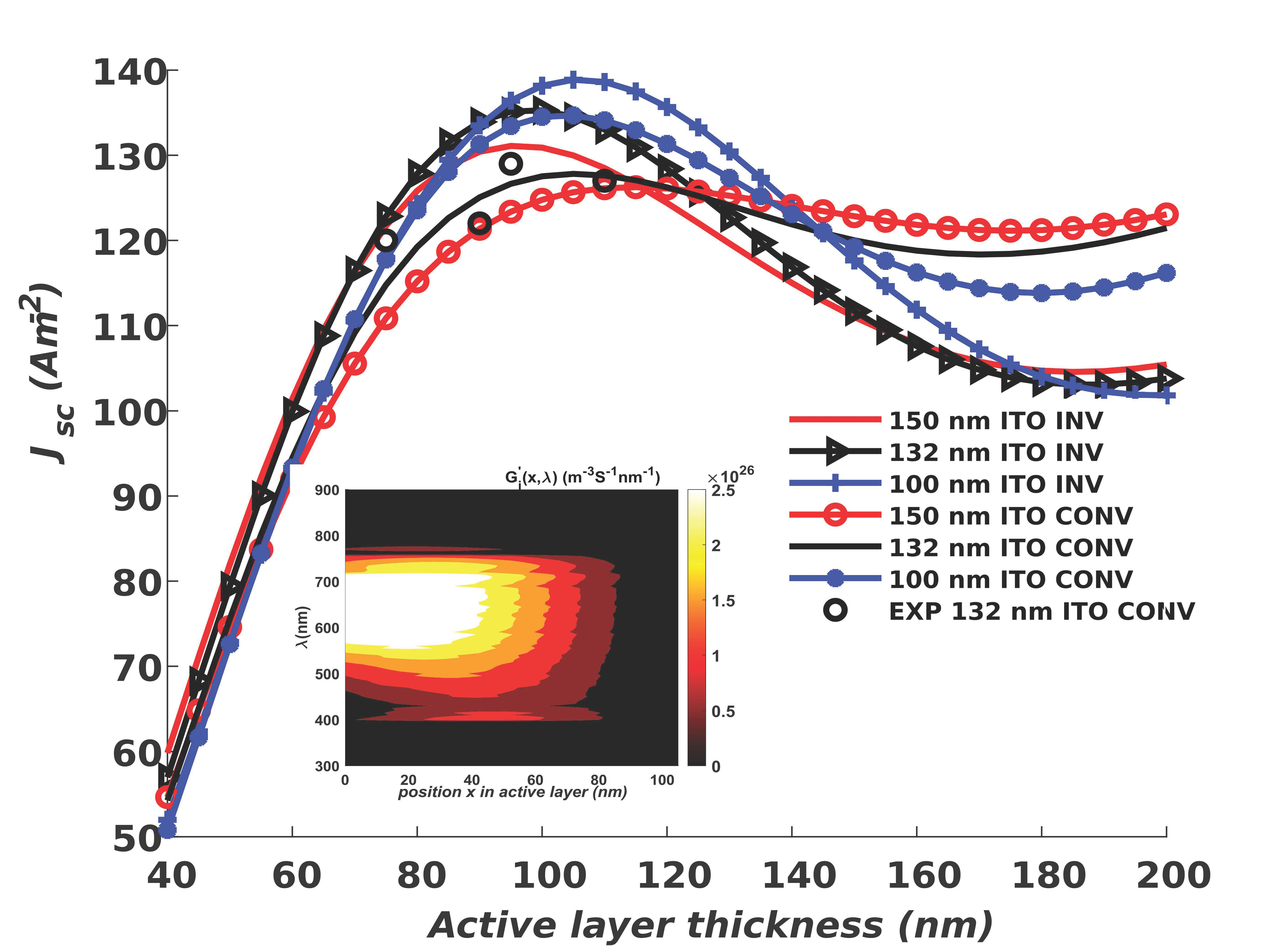
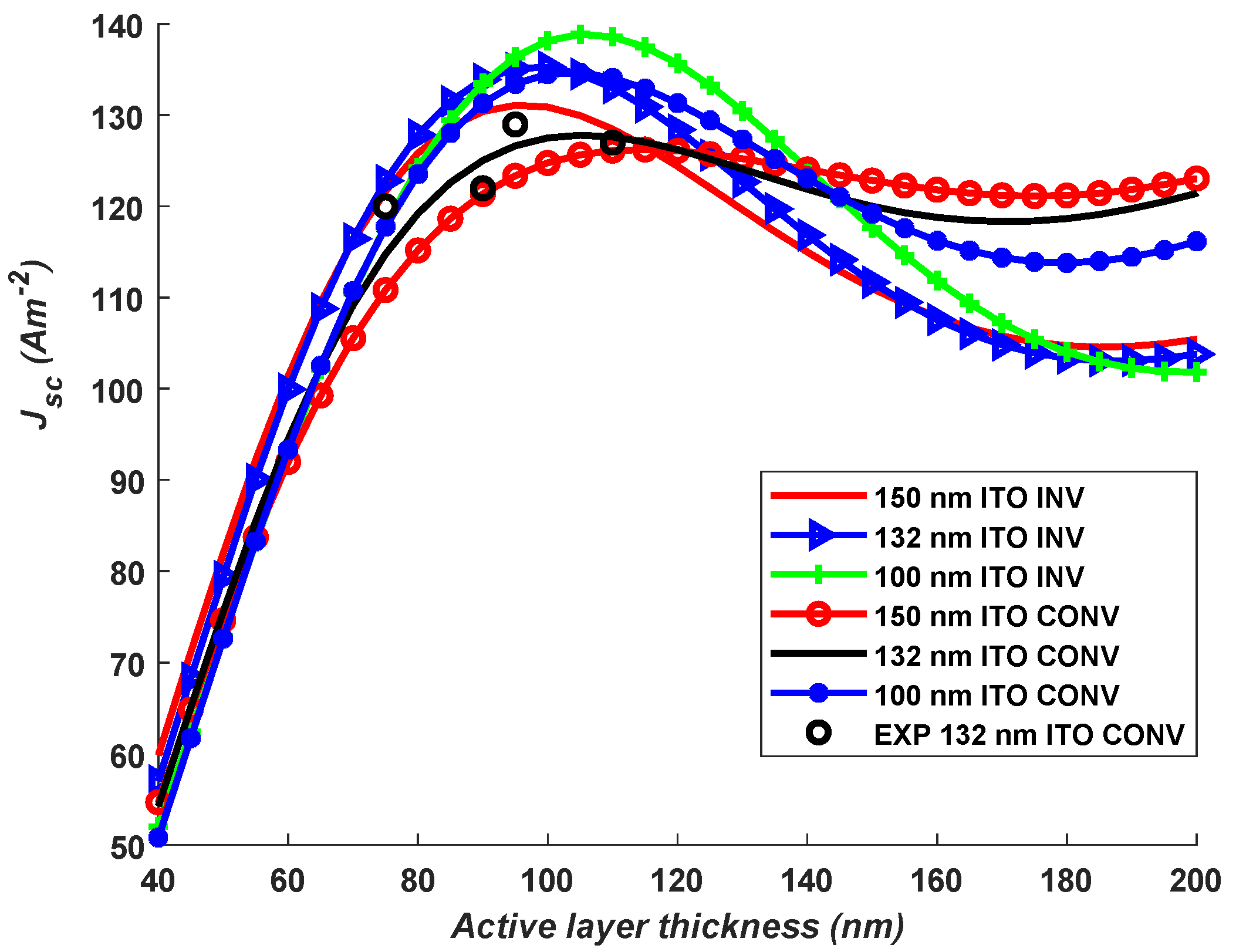
Simulation of the generation of free charge carriers from the absorption of solar photons in both conventional and inverted structure OSCs have been presented here for calculating the short circuit current density, J S C . The J S C thus obtained is optimised with respect to the thicknesses of the active layer and ITO in both conventional and inverted structures; however, it is optimised with respect to the thicknesses of the hole and electron layers only in the inverted structure. The results of these optimizations are described below.

3.1. Optimisation of J S C with Respect to ITO Thickness in Conventional and Inverted PTB7-Th:PNDI-T10 OSCs

Using the input parameters listed in Table 1 and indices of refraction and extinction coefficients of the active layer obtained from experiments [39], we simulated J S C in both the conventional and inverted OSCs with the same active layer blend of PTB7-Th:PNDIT10. Using three different ITO thicknesses of 150 nm, 132 nm, and 100 nm, the J S C of the conventional OSC of structure ITO/SiO2(20 nm)/PEDOT:PSS(40 nm)/PTB7-Th:PNDIT-10 (40 nm–200 nm)/LiF (1 nm)/Al (100 nm) and that of the inverted OSCs of structure ITO/SiO2 (20 nm)/Al (1 nm)/PTB7-Th:PNDI-T10 (40 nm–200 nm)/MoO3 (14 nm)/Ag (100 nm) were simulated and are plotted in Figure 3 as a function of the thickness of the active layer. For comparison, in Figure 3, we also show the experimental results of J S C measured in the conventional OSC for four active layer thicknesses of 75, 90, 95, and 110 nm with the ITO thickness of 132 nm [39].
According to Figure 3, our simulated J S C was 127 Am−2 at the active layer thickness of the 95-nm and 132-nm-thick ITO layer, which agrees quite well with the corresponding experimental value of 129 Am−2 [39]. Likewise, for the active layer thickness of 110 nm, both the simulated and experimental J S C had the same value of 127 Am−2 for the same ITO thickness of 132 nm. These agreements between the simulation and experimental results clearly validate our simulation method.
Having proven that our simulation was valid, we then wanted to optimize J S C with respect to the thickness of the ITO layer in order to optimise J S C in the conventional OCS. According to Figure 3, the maximum simulated   J S C = 135 Am−2 was found to be at an ITO thickness of 100 nm and the active layer thickness of 105 nm in a conventional OSC. As the peak in Figure 3 is relatively wider, one may consider optimal thickness of the active layer in the range of 90 nm to 110 nm and ITO thickness of 100 nm to generate higher J S C .
In the inverted OSC, according to Figure 3, the maximum simulated J S C = 139 Am−2 was also obtained at the same active layer thickness of 105 nm and ITO thickness of 100 nm. Thus, similar to the conventional OSC, as the peak of J S C was wider, an optimal active layer thickness in the range 90 nm to 115 nm was used. It was also distinctively conclusive that the inverted OSC gave a higher J S C than the conventional OSC, which also agreed with the experimental result [52].

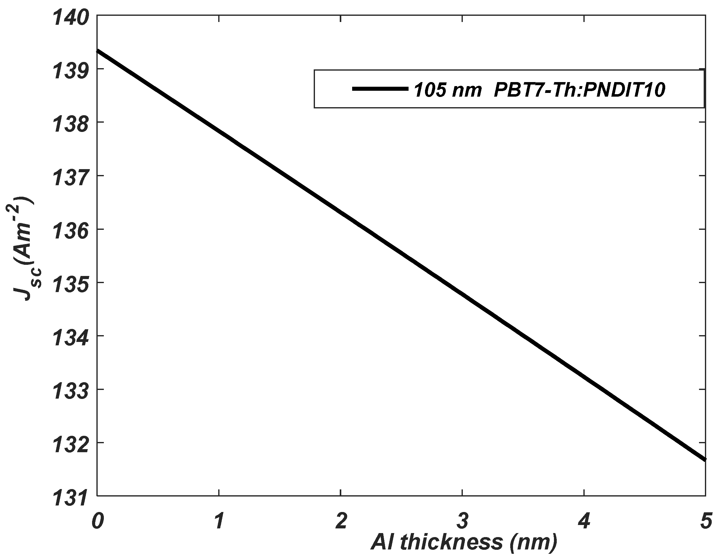
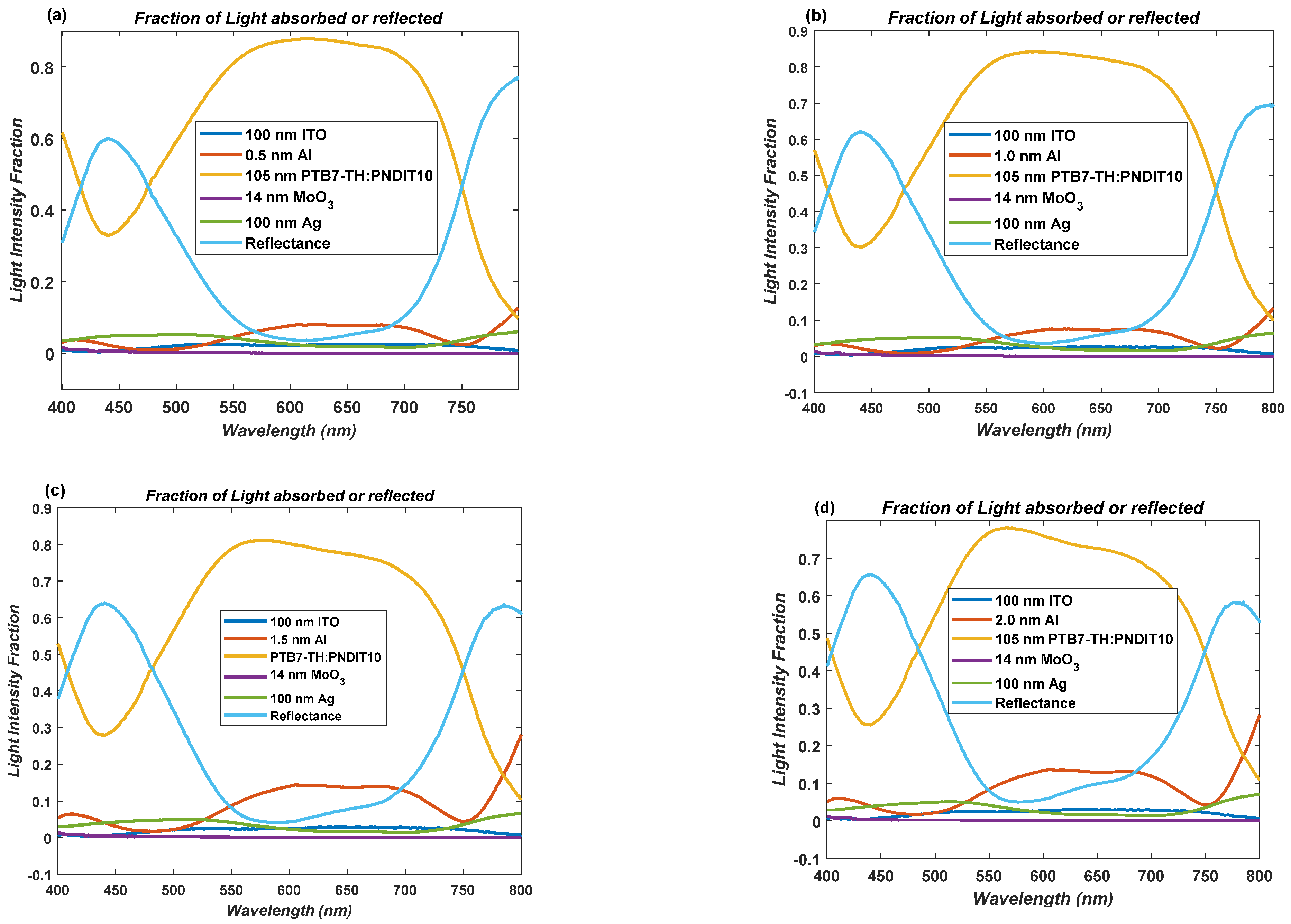
3.2. Optimizing Thickness of Al in Inverted OSC

In this section, we present the optimization of J S C with respect to the thickness of the Al layer (electron transport layer) in the inverted OSC. We plotted J S C as a function of the thickness of the Al layer, keeping the active layer thickness at 105 nm in Figure 4, which shows clearly that J S C decreased nearly linearly when the thickness of the Al layer increased from 0 to 5 nm. This was because, in the inverted structure, the light passed through the Al layer to be absorbed in the active layer; hence, the Al layer should be as transparent as possible. By increasing the thickness of the Al layer, absorption in this layer increased, which reduced the absorption in the active layer and, hence, reduced J S C . Therefore, the thickness of the Al layer should be very minimal to allow the transport of electrons to the cathode. Accordingly, the thickness of the Al layer should not exceed a few nms. This is consistent with the experimental results, where the Al thickness used was about 1.2 nm [53].

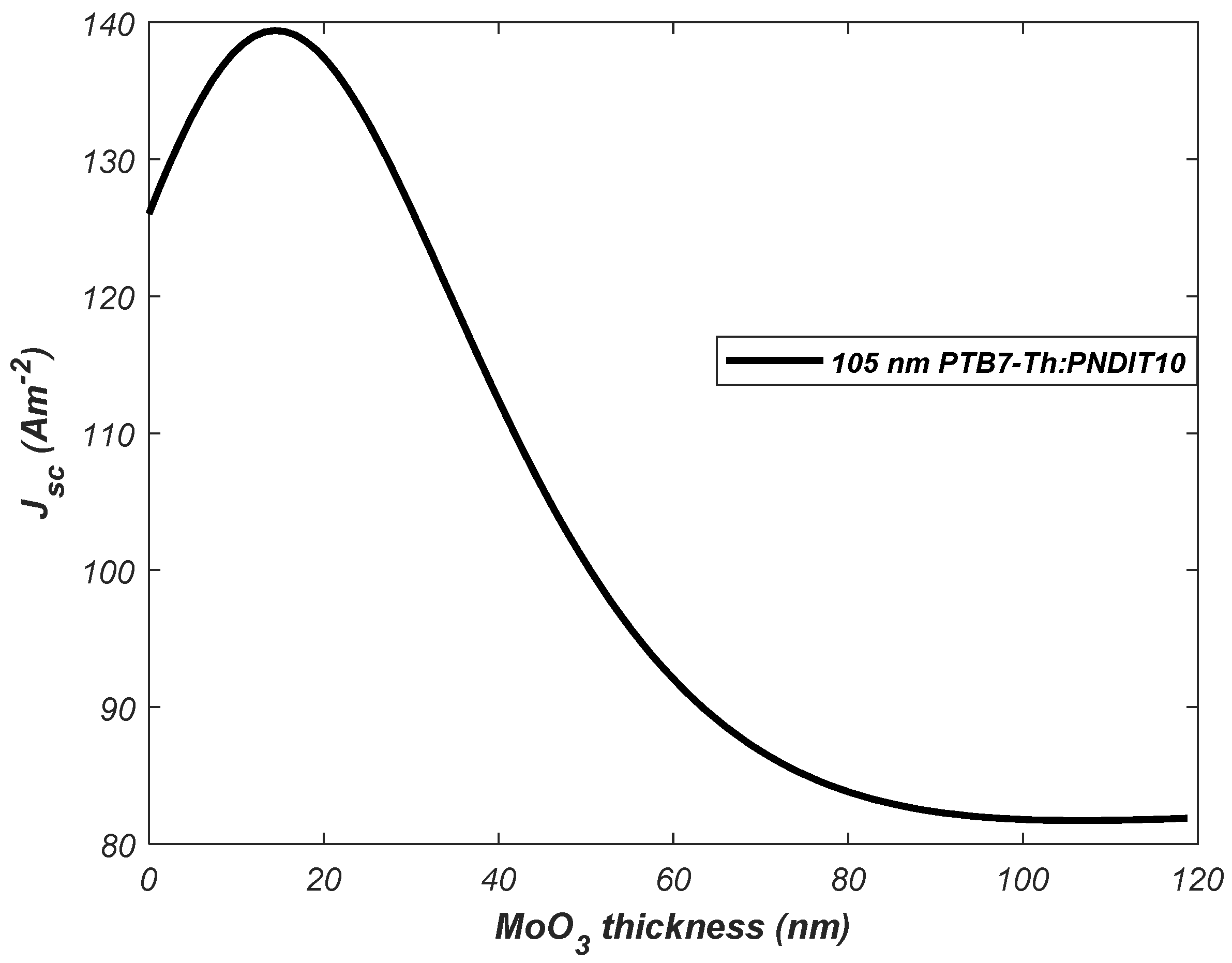
3.3. Optimizing Thickness of MoO3: The Hole Transport Layer in Inverted OSC

Using a cathode thickness of 100 nm ETL thicknesses of 0.5 nm, we plotted J S C in Figure 5 as a function of the thickness of the MoO3 layer, keeping the active layer thickness at 105 nm. According to Figure 5, an optimal J S C was obtained if the thickness of the MoO3 layer was between 14 nm to 25 nm. Such a thickness of MoO3 was a little larger than the 10 nm obtained by simulation with a different active layer and used in experiments as 3 nm and 5 nm [54], which also used different active layers involving a fullerene acceptor. This implies that the optimal thickness of the MoO3 layer may depend on the material blend and the thickness of the active layer. The simulated, optimized structures thus obtained for both conventional and inverted OSCs are summarized in Table 2.

3.4. Optimizing the Wavelenght of Photons for Maximum Absorption

In Figure 6, we plotted the simulated absorption and reflection as a function of the wavelength of the incident irradiation in the inverted optimized OSC with ITO (100 nm), four Al thicknesses of 0.5 nm (Figure 6a), 1 nm (Figure 6b), 1.5 nm (Figure 6c), and 2 nm (Figure 6d), active layer blend of 105 nm, and MoO3 (14 nm). The thickness of Al was varied to ascertain if there was any preferred value yielding better absorption with respect to wavelength of solar radiation. According to Figure 6a–d, regardless of the selected four thicknesses of the Al layer, the absorption in the active layer was dominant within the wavelength of 550 nm (2.26 eV) to 700 nm (1.77 eV); below and above this range the reflection becomes dominant. The energy range of 1.77 eV to 2.56 eV covered nearly the whole visible region, which implies higher absorption in OSCs compared to that in inorganic Si solar cells. As a result, the thickness of the Al layer of 1 nm was chosen to be the optimal thickness in the discussions to follow, which agrees with the experimental value of 1.2 nm [53].

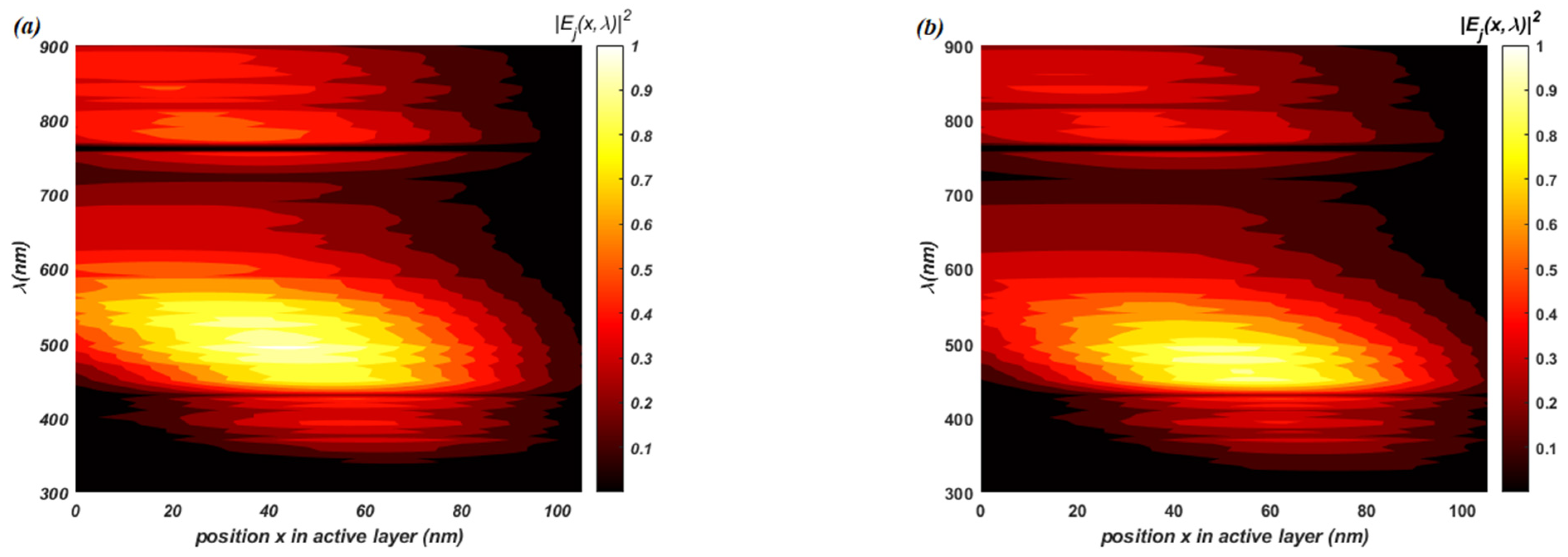
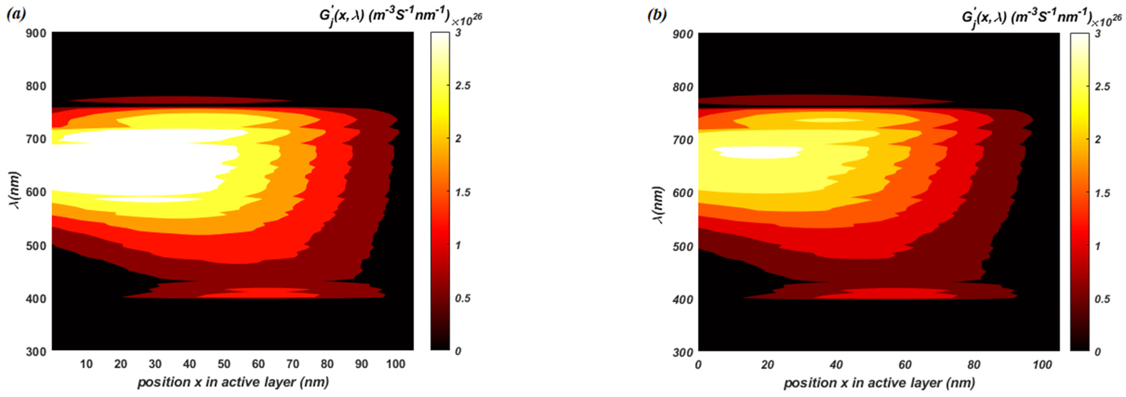
3.5. Electric Field Distribution and Exciton Generation Rate in Inverted and Conventional OSCs

Using Equation (1), we simulated the contour plots of the square modulus of the total electric field |   E j ( x ) | 2 as a function of the wavelength and position x within the active layer in both the conventional and inverted optimized OSCs of structures: (conventional) ITO (100 nm)/SiO2 (20 nm)/PEDOT:PSS (40 nm)/PTB7-Th:PNDI-T10 (105 nm)/LiF (1 nm)/Al (100 nm); (inverted): ITO (100 nm)/SiO2 (20 nm)/Al (1 nm)/PTB7-Th:PNDI-T10 (105 nm)/MoO3 (20 nm)/Ag (100 nm). The contour plots of electric field distribution within the active layer of conventional and inverted OSCs are shown in Figure 7a,b, respectively. In both figures, the spread of brighter spot represents the constructive interference position (CIP) between the forward and reflected electric field components, and both figures have only a single CIP with spread covering nearly the whole active layer. This was consistent with our earlier work [33] on different OSCs, where a single CIP was found within the active layer of 150 nm.
The CIPs represent positions of maximum photon activity, which can lead to maximum exciton generation at these points, where CIP overlaps with the region of maximum photon absorption in the active layer blend. It may be noted here that most generated excitons get dissociated within the active layer; therefore, the brighter spots represent the positions of generation of dissociated charge carriers within the active layer. The contour plots of the exciton generation rate G j ( x , λ ) in Equation (5) are plotted in Figure 8a,b as a function of position in the active layer and wavelength of solar radiation for conventional and inverted OSCs, respectively. It is evident from the plots in Figure 8a,b that more charge carriers were generated near the transparent electrode in both solar cells, which was obvious because the light was incident from the ITO side. Since the hole mobility was one order of magnitude higher than the electron mobility, as shown in Table 1, the charge carrier generation near the cathode (ITO) in the inverted OSC facilitated efficient extraction of the photogenerated electrons and holes in comparison with that in the conventional solar cell, where ITO was the anode. The exciton generation rate was also found to be higher in the inverted OSCs relative to that in the conventional OSCs due to the high reflectivity of MoO3/Ag in the inverted structure over LiF/Al in the conventional OSC. Thus, the higher J S C in the inverted OSC may be attributed to the combined effect of high reflectivity and exciton generation near the cathode in the inverted configuration.

4. Conclusions

Using the optical transfer matrix formalism, we optimized the layered structure of a conventional and an inverted BHJ OSCs with the active layer made of blended PTB7-Th:PNDI-T-10 by maximizing the J S C . The optimised structure thus obtained for both the OSCs is listed in Table 2. Maximum J S C thus obtained from the optimised structure of the inverted OSC is 139 Am−2 and that of the conventional OSC is 135 Am−2. Simulation of the electric field distribution in both inverted and conventional OSCs showed that the formation of a single CIP is obtained in the active layer of thickness 105 nm in both OSCs. As the light incidents from the ITO side, it was found that excitons are generated more closely to ITO electrode, which favors the efficient charge transport and collection at the opposite electrodes in the inverted OSC. This may be attributed to producing higher J S C   in the inverted OSC, as found here; hence, the inverted OSCs may be favored in future fabrications.

Author Contributions

D.D.Y.S. carried out the details of simulation work under the supervision of the corresponding author J.S.; H.M.R., N.K.E. and D.O. provided insight in MATLAB software and K.S.R. helped with the literature review. All authors have read and agreed to the published version of the manuscript.

Funding

This research received no external funding.

Data Availability Statement

The data presented in this study are available in this article.

Conflicts of Interest

The authors declare no conflict of interest.

References

  1. Xu, X.; Li, D.; Yuan, J.; Zhou, Y.; Zou, Y. Recent advances in stability of organic solar cells. ACS Energy Lett. 2021, 3, 100046. [Google Scholar] [CrossRef]
  2. You, Y.-J.; Saeed, M.A.; Shafian, S.; Kim, J.; Hyeon Kim, S.; Kim, S.H.; Kim, K.; Shim, J.W. Energy recycling under ambient illumination for internet-of-things using metal/oxide/metal-based colorful organic photovoltaics. Nanotechnology 2021, 32, 465401. [Google Scholar] [CrossRef] [PubMed]
  3. Ahsan Saeed, M.; Hyeon Kim, S.; Baek, K.; Hyun, J.K.; Youn Lee, S.; Won Shim, J. PEDOT:PSS: CuNW-based transparent composite electrodes for high-performance and flexible organic photovoltaics under indoor lighting. Appl. Surf. Sci. 2021, 567, 150852. [Google Scholar] [CrossRef]
  4. Sattar, A.; Farooq, M.; Amjad, M.; Saeed, M.A.; Nawaz, S.; Mujtaba, M.A.; Anwar, S.; El-Sherbeeny, A.M.; Soudagar, M.E.M.; Bandarra Filho, E.P.; et al. Performance Evaluation of a Direct Absorption Collector for Solar Thermal Energy Conversion. Energies 2020, 13, 4956. [Google Scholar] [CrossRef]
  5. Ganesamoorthy, R.; Sathiyan, G.; Sakthivel, P. Review: Fullerene based acceptors for efficient bulk heterojunction organic solar cell applications. Sol. Energy Mater. Sol. Cells 2017, 161, 102–148. [Google Scholar] [CrossRef]
  6. Green, M.A.; Hishikawa, Y.; Dunlop, E.D.; Levi, D.H.; Hohl-Ebinger, J.; Yoshita, M.; Ho-Baillie, A.W.Y. Solar cell efficiency tables (Version 53). Prog. Photovolt. 2019, 27, 3–12. [Google Scholar] [CrossRef] [Green Version]
  7. Girtan, M. Study of charge carriers’ transport in organic solar cells by illumination area shifting. Sol. Energy Mater. Sol. Cells 2017, 160, 430–434. [Google Scholar] [CrossRef]
  8. Sadoogi, N.; Rostami, A.; Faridpak, B.; Farrokhifar, M. Performance analysis of organic solar cells: Opto-electrical modeling and simulation. Eng. Sci. Technol. 2021, 24, 229–235. [Google Scholar] [CrossRef]
  9. Merritt, V.Y.; Hovel, H.J. Organic solar cells of hydroxy squarylium. Appl. Phys. Lett. 1976, 29, 414–415. [Google Scholar] [CrossRef]
  10. Kan, B.; Kan, Y.; Zuo, L.; Shi, X.; Gao, K. Recent progress on all-small molecule organic solar cells using small-molecule nonfullerene acceptors. InfoMat 2021, 3, 175–200. [Google Scholar] [CrossRef]
  11. Su, Y.-W.; Lan, S.-C.; Wei, K.-H. Organic photovoltaics. Mater. Today 2012, 15, 554–562. [Google Scholar] [CrossRef]
  12. Benten, H.; Mori, D.; Ohkita, H.; Ito, S. Recent research progress of polymer donor/polymer acceptor blend solar cells. J. Mater. Chem. A 2016, 4, 5340–5365. [Google Scholar] [CrossRef] [Green Version]
  13. Tang, C.W.; Albrecht, A.C. Photovoltaic effects of metal–chlorophyll-a–metal sandwich cells. J. Chem. Phys. 1975, 62, 2139–2149. [Google Scholar] [CrossRef]
  14. Singh, J.; Ruda, H.E.; Narayan, M.R.; Ompong, D. Concept of Excitons. In Optical Properties of Materials and Their Applications; John Wiley & Sons: Hoboken, NJ, USA, 2019; pp. 129–155. [Google Scholar]
  15. Tang, C.W. Two-layer organic photovoltaic cell. Appl. Phys. Lett. 1986, 48, 183–185. [Google Scholar] [CrossRef]
  16. Singh, J.; Narayan, M.; Ompong, D.; Zhu, F. Dissociation of charge transfer excitons at the donor–acceptor interface in bulk heterojunction organic solar cells. J. Mater. Sci. Mater. Electron. 2017, 28, 7095–7099. [Google Scholar] [CrossRef]
  17. Yu, G.; Gao, J.; Hummelen, J.C.; Wudl, F.; Heeger, A.J. Polymer Photovoltaic Cells: Enhanced Efficiencies via a Network of Internal Donor-Acceptor Heterojunctions. Science 1995, 270, 1789–1791. [Google Scholar] [CrossRef] [Green Version]
  18. Narayan, M.R.; Singh, J. Study of the mechanism and rate of exciton dissociation at the donor-acceptor interface in bulk-heterojunction organic solar cells. J. Appl. Phys. 2013, 114, 073510. [Google Scholar] [CrossRef] [Green Version]
  19. Yin, H.; Yan, C.; Hu, H.; Ho, J.K.W.; Zhan, X.; Li, G.; So, S.K. Recent progress of all-polymer solar cells—From chemical structure and device physics to photovoltaic performance. Mater. Sci. Eng. R Rep. 2020, 140, 100542. [Google Scholar] [CrossRef]
  20. Liu, Q.; Jiang, Y.; Jin, K.; Qin, J.; Xu, J.; Li, W.; Xiong, J.; Liu, J.; Xiao, Z.; Sun, K.; et al. 18% Efficiency organic solar cells. Sci. Bull. 2020, 65, 272–275. [Google Scholar] [CrossRef] [Green Version]
  21. Ullah, F.; Chen, C.-C.; Choy, W.C.H. Recent Developments in Organic Tandem Solar Cells toward High Efficiency. Adv. Sustain. Syst. 2021, 2, 2000050. [Google Scholar] [CrossRef]
  22. Ameri, T.; Dennler, G.; Lungenschmied, C.; Brabec, C.J. Organic tandem solar cells: A review. Energy Environ. Sci. 2009, 2, 347–363. [Google Scholar] [CrossRef]
  23. Vos, A.D. Detailed balance limit of the efficiency of tandem solar cells. J. Phys. D 1980, 13, 839–846. [Google Scholar] [CrossRef]
  24. Müller, R.; Schygulla, P.; Lackner, D.; Höhn, O.; Hauser, H.; Richter, A.; Fell, A.; Bläsi, B.; Predan, F.; Benick, J.; et al. Silicon-based monolithic triple-junction solar cells with conversion efficiency >34%. In Proceedings of the 37th European Photovoltaic Solar Energy Conference and Exhibition, Lisboa, Portugal, 9–11 September 2020; pp. 574–578. [Google Scholar] [CrossRef]
  25. Wang, J.; Zheng, Z.; Zu, Y.; Wang, Y.; Liu, X.; Zhang, S.; Zhang, M.; Hou, J. A Tandem Organic Photovoltaic Cell with 19.6% Efficiency Enabled by Light Distribution Control. Adv. Mater. 2021, 33, 2102787. [Google Scholar] [CrossRef] [PubMed]
  26. Zhang, K.; Ying, L.; Yip, H.L.; Huang, F.; Cao, Y. Toward Efficient Tandem Organic Solar Cells: From Materials to Device Engineering. ACS Appl. Mater. Interfaces 2020, 12, 39937–39947. [Google Scholar] [CrossRef] [PubMed]
  27. Sreedhar Ram, K.; Singh, J. Over 20% Efficient and Stable Non-Fullerene-Based Ternary Bulk-Heterojunction Organic Solar Cell with WS2 Hole-Transport Layer and Graded Refractive Index Antireflection Coating. Adv. Theory Simul. 2020, 3, 2000047. [Google Scholar] [CrossRef]
  28. Xiong, M.; Wu, J.; Fan, Q.; Liu, Q.; Lv, J.; Ou, X.; Guo, X.; Zhang, M. Ternary organic solar cells with improved efficiency and stability enabled by compatible dual-acceptor strategy. Org. Electron. 2021, 96, 106227. [Google Scholar] [CrossRef]
  29. Wang, Z.S.; Ren, X.; Xu, X.; Peng, Q.; Sha, W.E.I.; Choy, W.C.H. A comprehensively theoretical and experimental study of carrier generation and transport for achieving high performance ternary blend organic solar cells. Nano Energy 2018, 51, 206–215. [Google Scholar] [CrossRef]
  30. Mulligan, C.J.; Wilson, M.; Bryant, G.; Vaughan, B.; Zhou, X.J.; Belcher, W.J.; Dastoor, P.C. A projection of commercial-scale organic photovoltaic module costs. Sol. Energy Mater. Sol. Cells 2014, 120, 9–17. [Google Scholar] [CrossRef]
  31. Gagliardi, A.; Wang, S.; Albes, T. Simulation of charge Carrier mobility unbalance in organic solar cells. Org. Electron. 2018, 59, 171–176. [Google Scholar] [CrossRef]
  32. Burlingame, Q.; Loo, Y.L. Optical simulations to inform the design of UV-absorbing organic materials and solar cells. Sol. Energy Mater. Sol. Cells 2021, 227, 111114. [Google Scholar] [CrossRef]
  33. Mehdizadeh Rad, H.; Zhu, F.; Singh, J. Profiling exciton generation and recombination in conventional and inverted bulk heterojunction organic solar cells. J. Appl. Phys. 2018, 124, 083103. [Google Scholar] [CrossRef]
  34. Pettersson, L.A.A.; Roman, L.S.; Inganäs, O. Modeling photocurrent action spectra of photovoltaic devices based on organic thin films. J. Appl. Phys. 1999, 86, 487–496. [Google Scholar] [CrossRef]
  35. Sreedhar Ram, K.; Mehdizadeh-Rad, H.; Ompong, D.; Setsoafia, D.D.Y.; Singh, J. Characterising Exciton Generation in Bulk-Heterojunction Organic Solar Cells. Nanomaterials 2021, 11, 209. [Google Scholar] [CrossRef] [PubMed]
  36. Sreedhar Ram, K.; Ompong, D.; Rad, H.M.; Setsoafia, D.D.Y.; Singh, J. An Alternative Approach to Simulate the Power Conversion Efficiency of Bulk Heterojunction Organic Solar Cells. Phys. Status Solidi A 2020, 218, 2000597. [Google Scholar] [CrossRef]
  37. Xu, Y.; Yuan, J.; Liang, S.; Chen, J.-D.; Xia, Y.; Larson, B.W.; Wang, Y.; Su, G.M.; Zhang, Y.; Cui, C.; et al. Simultaneously Improved Efficiency and Stability in All-Polymer Solar Cells by a P–i–N Architecture. ACS Energy Lett. 2019, 4, 2277–2286. [Google Scholar] [CrossRef]
  38. Wang, G.; Melkonyan, F.S.; Facchetti, A.; Marks, T.J. All-Polymer Solar Cells: Recent Progress, Challenges, and Prospects. Angew. Chem. Int. Ed. 2019, 58, 4129–4142. [Google Scholar] [CrossRef] [PubMed]
  39. Li, Z.; Xu, X.; Zhang, W.; Meng, X.; Ma, W.; Yartsev, A.; Inganas, O.; Andersson, M.R.; Janssen, R.A.; Wang, E. High Performance All-Polymer Solar Cells by Synergistic Effects of Fine-Tuned Crystallinity and Solvent Annealing. J. Am. Chem. Soc. 2016, 138, 10935–10944. [Google Scholar] [CrossRef] [PubMed]
  40. Burkhard, G.F.; Hoke, E.T.; McGehee, M.D. Accounting for interference, scattering, and electrode absorption to make accurate internal quantum efficiency measurements in organic and other thin solar cells. Adv. Mater. 2010, 22, 3293–3297. [Google Scholar] [CrossRef] [PubMed]
  41. Monestier, F.; Simon, J.J.; Torchio, P.; Escoubas, L.; Ratier, B.; Hojeij, W.; Lucas, B.; Moliton, A.; Cathelinaud, M.; Defranoux, C.; et al. Optical modeling of organic solar cells based on CuPc and C60. Appl. Opt. 2008, 47, C251–C256. [Google Scholar] [CrossRef]
  42. Hoppe, H.; Arnold, N.; Sariciftci, N.S.; Meissner, D. Modeling the optical absorption within conjugated polymer/fullerene-based bulk-heterojunction organic solar cells. Sol. Energy Mater. Sol. Cells 2003, 80, 105–113. [Google Scholar] [CrossRef]
  43. Zhao, X.; Mi, B.; Gao, Z.; Huang, W. Recent progress in the numerical modeling for organic thin film solar cells. Sci. China Phys. Mech. 2011, 54, 375–387. [Google Scholar] [CrossRef]
  44. Braun, C.L. Electric field assisted dissociation of charge transfer states as a mechanism of photocarrier production. J. Chem. Phys. 1984, 80, 4157–4161. [Google Scholar] [CrossRef]
  45. Vollbrecht, J.; Brus, V.V.; Ko, S.J.; Lee, J.; Karki, A.; Cao, D.X.; Cho, K.; Bazan, G.C.; Nguyen, T.Q. Quantifying the Nongeminate Recombination Dynamics in Nonfullerene Bulk Heterojunction Organic Solar Cells. Adv. Energy Mater. 2019, 9, 12. [Google Scholar] [CrossRef]
  46. Hughes, M.P.; Rosenthal, K.D.; Ran, N.A.; Seifrid, M.; Bazan, G.C.; Nguyen, T.Q. Determining the Dielectric Constants of Organic Photovoltaic Materials Using Impedance Spectroscopy. Adv. Funct. Mater. 2018, 28, 1801542. [Google Scholar] [CrossRef]
  47. Islam, M.S. Analytical modeling of organic solar cells including monomolecular recombination and carrier generation calculated by optical transfer matrix method. Org. Electron. 2017, 41, 143–156. [Google Scholar] [CrossRef]
  48. Jeckelmann, B.; Piquemal, F. The Elementary Charge for the Definition and Realization of the Ampere. Ann. Phys. 2018, 531, 1800389. [Google Scholar] [CrossRef] [Green Version]
  49. Steiner, R. History and progress on accurate measurements of the Planck constant. Rep. Prog. Phys. 2012, 76, 016101. [Google Scholar] [CrossRef] [PubMed]
  50. Porrat, D.; Bannister, P.R.; Fraser-Smith, A.C. Modal phenomena in the natural electromagnetic spectrum below 5 kHz. Radio Sci. 2001, 36, 499–506. [Google Scholar] [CrossRef]
  51. Pitre, L.; Plimmer, M.D.; Sparasci, F.; Himbert, M.E. Determinations of the Boltzmann constant. C.R. Phys. 2019, 20, 129–139. [Google Scholar] [CrossRef]
  52. Lee, Y.-J.; Adkison, B.L.; Xu, L.; Kramer, A.A.; Hsu, J.W.P. Comparison of conventional and inverted organic photovoltaic devices with controlled illumination area and extraction layers. Sol. Energy Mater. Sol. Cells 2016, 144, 592–599. [Google Scholar] [CrossRef] [Green Version]
  53. Kam, Z.; Yang, Q.; Wang, X.; Wu, B.; Zhu, F.; Zhang, J.; Wu, J. Enhanced absorbance and electron collection in inverted organic solar cells: Optical admittance and transient photocurrent analyses. Org. Electron. 2014, 15, 1306–1311. [Google Scholar] [CrossRef]
  54. Tao, C.; Ruan, S.; Zhang, X.; Xie, G.; Shen, L.; Kong, X.; Dong, W.; Liu, C.; Chen, W. Performance improvement of inverted polymer solar cells with different top electrodes by introducing a MoO3 buffer layer. Appl. Phys. Lett. 2008, 93, 411. [Google Scholar] [CrossRef]
Figure 1. The structure of PTB7-Th polymer donor and PNDI-T10 acceptor polymer [39].
Energies 15 00711 g001
Figure 2. Schematic diagram of an organic solar cell stack, indicating light incident from the left side of the device. Starting from the left, the layers are indexed as j = 0 starting with the glass substrate to j = m + 1 for the air medium (far right beyond the OSC). E is the electric field of the electromagnetic radiation propagating through the device. E j + and E j are the forward and reflected components of E at each interface, respectively; dj represents the thickness of the jth layer’ and R and T represent, respectively, reflection and transmission of E through the whole device.
Energies 15 00711 g002
Figure 3. Simulated J S C is plotted for both conventional and inverted OSCs as a function of the active layer thickness for three selected ITO thicknesses of 100 nm, 132 nm, and 150 nm. The experimental results are also plotted for comparison.
Energies 15 00711 g003
Figure 4. J S C plotted as a function of the Al film thicknesses up to 5 nm in the inverted OSC by keeping the thickness of the active layer at 105 nm.
Energies 15 00711 g004
Figure 5. J S C of inverted OSC plotted as a function of the MoO3 layer at an active layer thickness of 105 nm and Al layer thickness of 1 nm.
Energies 15 00711 g005
Figure 6. Absorption and reflection plotted as a function of the wavelength of the incident solar radiation in the inverted OSC with the structure: ITO(100 nm), Al (x nm) active layer blend (105 nm), and MoO3 (20 nm), where (a) x = 0.5 nm, (b) x = 1.0, (c) x = 1.5, and (d) x = 2.0.
Energies 15 00711 g006
Figure 7. Contour plots of the electric field distribution | E j ( x ) | 2 as a function of x and λ in (a) inverted and (b) in conventional OSCs.
Energies 15 00711 g007
Figure 8. Contour plots of the exciton generation as a function of x and   λ in (a) inverted and (b) conventional OSCs.
Energies 15 00711 g008
Table 1. Input and fitting parameters used in the simulation.
ParameterValueReferences
Lj (nm)40–200[36]
εr3.4[46]
µn (m2V−1s−1)6.0 × 10⁻⁴[39]
µp (m2V−1s−1)1.0 × 10⁻³
ρ (Ωcm)1000[35]
n(cm 3)2 × 10²²
Vbi (eV)0.8 (1.1)[47]
Ntbulk (m−3)2.1 × 10¹⁹ [45]
Ntsurf (m−2)6.3 × 10¹⁸
T (K)300[36]
e (C)1.6 × 10⁻¹⁹[48]
h (Js−1)6.63 × 10⁻³⁴[49]
ε0 (Fm−1)8.85 × 10⁻¹²[50]
k (JK−1)1.3840 × 10⁻²³[51]
ζ 5.29 × 10⁻¹⁴ (fitting parameter)
λ1 (nm)300
λ2 (nm) 900
Table 2. Summary of the optimized components of the inverted and conventional OSC.
Inverted OSCConventional OSC
LayersOptimized Thickness (nm)
ITO (Cathode/Anode)100100
Al (ETL)1
PTB7-Th:PNDI-T10 (ATL)85–12590–115
MoO3 (HTL)14–25
Publisher’s Note: MDPI stays neutral with regard to jurisdictional claims in published maps and institutional affiliations.

