1. Introduction
Semiconductor materials are still the dominating components of solar cells. The photovoltaic (PV) market is currently based on crystalline silicon (c-Si) technologies, mainly as a result of their low fabrication costs and high reliability of the material and the fabrication processes. Research cell record efficiencies are approaching 27% therefore, toward a 29.4% theoretical limit for c-Si solar cells, only minor improvements are possible [
1,
2].
In a semiconductor material, photons from the absorbed light give their energy to electrons from the valence band, which then move to the conduction band. However, this only happens when the photons have an energy greater than the semiconductor’s energy band gap, which is a characteristic value of the semiconductor. On the other hand, the excess of photon energy (resulting from the difference between the photon energy and the absorber gap energy value) is lost in the thermalization process—energy higher than the band gap excites electrons in the absorber area, and then its excess is unproductively lost. Therefore, the effect of limiting the efficiency of solar cells with a low band gap energy is a compromise between the amount of photons absorbed by the semiconductor and the simultaneous thermal loss, which can be solved by introducing a second absorber with a higher band gap energy [
3]. An effective solution seems to be to use more than one absorber with a different energy band gaps, as in the case of multijunction solar cells, and thus reduce internal losses. In such a system, a surface cell with a higher band gap reduces the amount of losses resulting from the thermalization phenomenon, and the lower absorber absorbs the rest of the unabsorbed light [
2]. This allows for more effective operation and sharing of the solar radiation spectrum, which consequently leads to an increase in the photovoltaic conversion efficiency (PCE) [
4].
Recently, one of the most popular examples of a multijunction solar cell, characterized by its simple configuration, is the tandem solar cell (TSC). Considering that cheap and efficient solar cells based on c-Si silicon are the most popular because of their low band gap energy of 1.1 eV and high open circuit voltage (V
OC) up to 750 mV, therefore, they are a great material to use as a bottom cell in TSC [
2]. Moreover, the combination of silicon with a perovskite cell in a tandem enables an increase in efficiency above 30%, at the same time reducing the cost of 1 kWp [
5]. Inorganic–organic perovskites such as, for example, metal halides, seem promising in this role. Due to high absorption, they have been the subject of research for over 7000 publications submitted by the end of 2019 [
4]. Such a turn of events caused a simultaneous increase in interest in silicon/perovskite tandem cells, the efficiency of which exceeded 25% within three years of development [
2].
Basically, there are two views of a tandem link. The so called 4-terminal structure is mechanically stacked tandem with a Si or copper indium gallium (di)selenide (CIGS) as the bottom cell and perovskite solar cell as the top cell. In contrast, a 2-terminal or monolithic tandem consists of two series-connected sub-cells [
6].
The most simple to implement tandem solar cell configuration is a 4-terminal (4T) construction. Two separately made cells allows problems to be avoided related to the temperature of the process and the choice of solvent, substrate roughness, or polarity of the cell, especially in the case of the top cell. Additionally, it is possible to precisely control the band gap and to approach the optimal value as much as possible [
2]. An additional advantage of 4T cells is the lack of the need to adjust the current of individual cells, because they do not have to be connected in series, and this allows for a wide range of tuning the band gap [
7]. 4T cells are easier to configure, but their disadvantages are the presence of parasitic absorption and additional reflections from the interlayers, which must result in a TSC reduction in efficiency [
8]. This is why it is so important to develop layers and conductive electrodes with high transparency [
9].
Another more advanced example is the 2-terminal (2T) configuration. In this case, in order to avoid losses, the current between the cells should be adjusted, because 2T cells consist of two sub-cells connected in series [
8,
9]. The requirement of “current matching” narrows the range of the ideal band gap to 1.7–1.8 eV [
2]. The top cell in the 2T architecture with higher bandgap energy converts high energy photons at high voltage, while passing unabsorbed photons with an energy lower than the absorption edge. On the other hand, the bottom sub-cell converts the low-energy photons that reach it. According to Kirchhoff’s law, the effective voltage is the sum of the voltages of individual cells, and the photocurrent is limited by the lower current among the sub-cells [
2]. Additionally, to obtain a higher efficiency of the photovoltaic conversion, the lower parasitic absorption must be obtained by the reduction in losses from series resistance through the transport of lower current at higher voltage [
4]. In the 2T structure, it is necessary to use only two contacts including one (on the top sub-cell) transparent to light, therefore, the use of transparent electrodes is necessary and cannot be ignored [
3,
10,
11,
12]. Sub-cells in the 2T structure are connected by a tunnel junction or a recombination layer into a monolithic cell. The main difficulty is the selection of this layer between the cells, which should satisfy two conditions: to ensure low resistance of the series connection between the cells and, at the same time, to minimize optical losses through low light abortion inside this layer. Another research aspect is applying the top sub-cell in a way that does not affect the lower sub-cell. An interesting way is the TiN layer deposition in CZTS/Si (Cu
2ZnSnS
4/Si) tandem solar cell. This operation mitigates in-diffusion of CZTS elements into the c-Si bulk during the high temperature sulfurization process, forming both a diffusion barrier and recombination layer [
13]. Additionally, the lower sub-cell must be a suitable substrate for the application of the upper sub-cell, so the use of a silicon cell with a surface texture of more than 1 micron is a challenge [
2].
The losses in the silicon/perovskite-based TSC result from two categories: optical losses and electronic losses. The optical losses are mainly from the reflection from the surface, parasitic absorption on translucent contacts and intermediate layers, and incomplete absorption in the sub-cells. On the other hand, electronic losses result from the excitation of carriers which: (a) are not removed from the device, and (b) lose energy in the recombination process through non-radiative recombination pathways or non-ideal contact material [
3]. Designing a silicon/perovskite tandem cell also necessitates the appropriate length of the diffusion path for the upper cell so that the perovskite layer should be thick enough to absorb all photons with energy above the band gap in a single pass [
3]. Limiting these losses leads to an increase in the theoretical PCE limit to the value of 45% [
4,
14].
Perovskites are an ideal candidate for use in TSC. Their wide band gap energy of 1.48–2.23 eV, steep absorption edge, and low sub-band absorption enable connection with silicon [
15,
16]. Additionally, matching in the 2T structure is easy due to the simplicity of the control of the band gap energy and therefore ensuring current matching. Moreover, perovskite solar cells offer high V
OC with low potential loss, high defect tolerance, long charge carrier diffusion lengths, and photon recycling. Additionally, perovskites achieve high efficiencies, are cheap to obtain, and can be applied by a number of chemical and physical methods [
2]. Additionally, the problem of long-term stability of the perovskite has recently being solved in various research works. Much emphasis has been placed on device architecture, electron transport layer, hole transport layer, electrodes, and encapsulation [
17]. Apart from the subjects related to the composition change [
18,
19,
20] and functional layers [
21,
22,
23,
24], the encapsulation of tandem solar cells plays an increasingly important role, which certainly brings this technology closer to commercial applications such as typical silicon photovoltaic modules [
17,
25,
26].
The historically used and best known compound is methylammonium lead iodide (MALI) with a band gap energy equal to 1.55 eV. Obviously, this is not an ideal material for coexistence with silicon, but it was perfect for the first tests in 2T structures. Defining the perovskite as a material in which the energy of the band gap is easy to control, it is enough to emphasize that the substitution of iodine ions by bromine allows for the control of the band gap energy in the range of 1.55–2 eV [
2,
5,
27]. Unfortunately, this leads to a change in the crystal structure from trigonal to cubic, and for the composition close to this transition, the material shows amorphous properties with high levels of energetic disorder, unexpectedly low absorption and low charge-carrier mobilities. However, the additional substitution of MA
+ cations into Cs ions allows for the structure to be stabilize and achieve an absorber with a band gap energy equal to 1.75 eV [
16].
The problem of the perovskite layer thickness has already been addressed above. The absorber layer with a band gap energy of 1.75 eV should have a thickness of approx. 1 µm, which may be problematic for meeting the current matching criterion due to the preservation of high quality of the material [
2]. One of the aspects is to increase the size of the grains and the crystallinity of the structure, which increases the lifetime of the carriers, by introducing methyl ammonium chloride (MACl), which enables the grains to grow and, consequently, to reduce the number of grain boundaries [
28,
29].
One way to improve TSC performance is to use the amorphous silicon/crystalline silicon (SHJ) heterojunction through excellent spectral responsivity in the near-infrared spectral region. However, the temperature of the perovskite layer deposition is critical as it will not destroy the SHJ structure [
30]. The lowering of the current is also due to the use of double polished silicon, providing optical losses [
2]. In this case, the application of the perovskite (e.g., via spin-coating) is optimal. However, the introduction of texture, even one-sided (from the bottom of the cell) significantly improves the energy yield. The classic texture improves the absorption properties by reducing the reflection and works well in the 4T structure, but for 2T cells, it prevents the application of perovskite by wet chemistry methods without completely filling the space between the pyramids or pits [
30].
Deposition of a continuous layer of perovskite on the surface of the pyramidal texturized silicon may lead to an increase in the generated photocurrent to the level of >20 mAcm
−2 [
2]. Sahli et al. deposited porous perovskite by co-evaporation of lead iodide and caesium bromide, and then spin-coated an organohalide solution (formamidine iodide, FAI and formamidine bromide, FABr), which infiltrated the pores and did not form organohalides in the valleys of the pyramids [
31]. Unfortunately, the quality of the applied perovskite layer did not allow a satisfactory fill factor (FF) parameter to be achieved. Another method was co-evaporation, which fully enables the formation of a conformal layer on the surface of the pyramids. It is a method that requires tremendous control of the deposition rate due to the large difference in vapor pressure between the organic and inorganic components. However, composing the perovskite layer requires the use of at least four sources, and the vacuum-deposited perovskites have not yet achieved the same cell efficiency as their solution processed counterparts [
32].
The literature has already reported successful attempts to cover a silicon cell with a pyramidal texture with a size of about 1 µm. Thus, the problem of uncovered pyramids and ineffective separation of the charge on different thicknesses of the perovskite layer has been overcome. Hou et al. used a concentrated precursor (1.65–1.75 M) that allowed for the creation of a perovskite layer with a thickness of a micrometer and a grain size of 2–4 mm [
33]. In turn, Chen et al., through a high-throughput blade coating, applied perovskite to a textured silicon surface with a controlled and reduced pyramid height below 2 µm. In this way, the perovskite layer planarized the textured surface and its thickness was below 2 µm [
32]. Both achievements led to complete coverage of the pyramids, resulting from the silicon texturization by the applied perovskite layer. For this reason, optical losses were minimized by reducing the reflection from the textured bottom cell, which in turn is important for meeting the current matching condition.
This paper discusses the problem of wet perovskite incorporation into the porous structure of silicon in the form of chemically etched wires. All preparation methods are based on wet chemistry, intentionally leading to production by fast and cheap processes that can be easily commercialized. The novelty of this work is the combination of the Si wire structure with a typical perovskite layer to simultaneously ensure a bottom cell reflectance reduction and a porous scaffold for the top cell.
3. Results
Chemical texturization of silicon can serve not only to increase roughness to reduce solar reflection, but also to provide a porous scaffold for the perovskite layer. One of the common techniques for obtaining high-performance perovskite cells is to apply or print a porous layer of titanium dioxide. On such a structure of pores and on the surface, a layer of perovskite absorber is deposited by wet methods. The authors propose the use of porous silicon structures instead of porous TiO2 to create a tandem cell.
This paper deals with the microstructure of the silicon-perovskite transition zone, but the authors first performed a series of analyses to define the structures of the tandem solar cell as a whole. In Lumerical FDTD solution, simulations were made to estimate the level of absorption in the individual layers of the tandem cell depending on the wavelength of the electromagnetic radiation (
Figure 1). Preliminary studies have been performed, which consist of selecting materials for individual cells in the case of the band gap energies. Moreover, the chosen type of material was matched to individual sub-cells and the level of absorption in individual layers was simulated. The simulation showed how the thickness of individual layers influences the absorption in the photoactive material of each sub-cell.
The simulations were carried out for the basic system containing silicon with an ITO and Au layer as a recombination layer, a perovskite layer, and another ITO as a transparent electrode (
Figure 1a). It has been shown that matching of the perovskite to silicon at the energy level corresponds to the areas of effective light absorption. The perovskite absorbed high-energy radiation because of the higher energy gap while the transmitted radiation with lower energy was effectively absorbed by the silicon (
Figure 1b). Modeling was also based on matching the energy gaps of individual absorbers to obtain the most effective structure possible. Since the silicon energy gap is strictly defined and unchanging, it was necessary to use the ability to control the energy gap of the perovskite by, for example, changing the chemical composition.
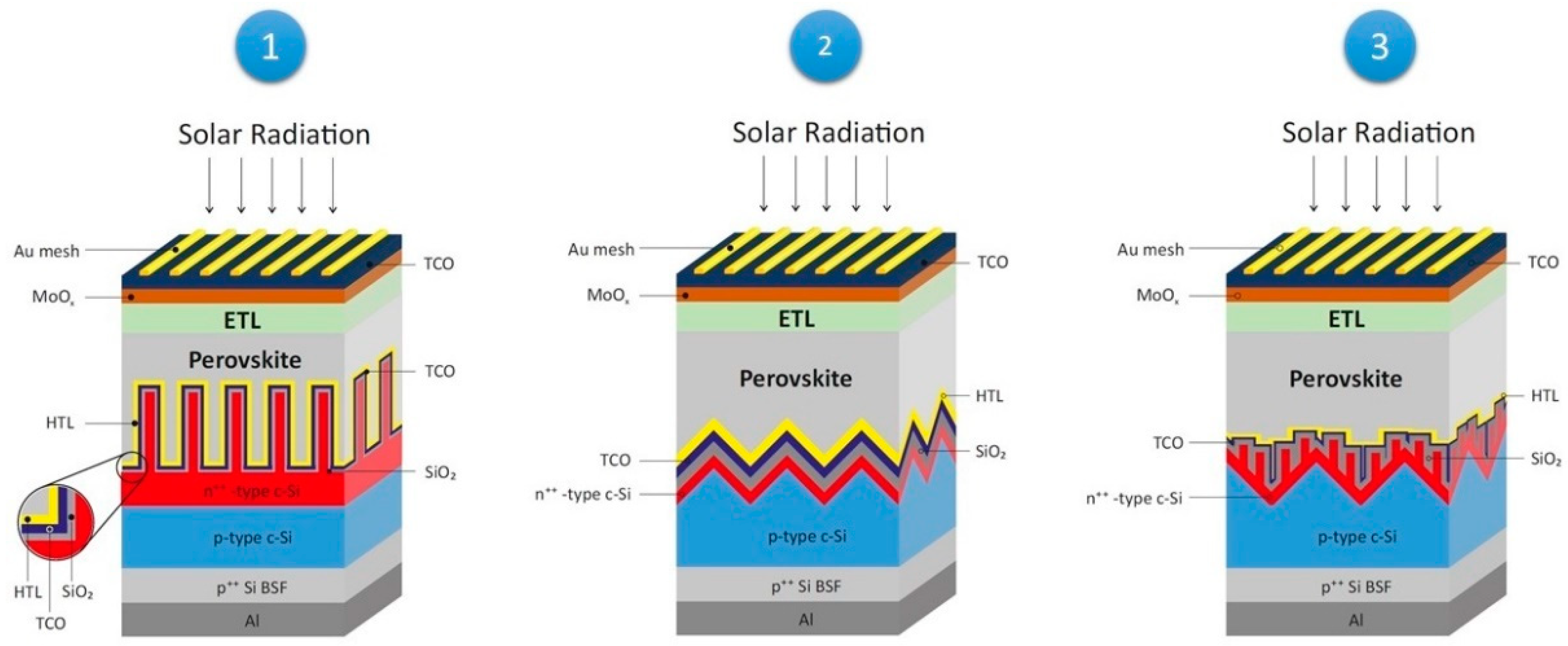
After the simulations, the authors changed the composition of the tandem solar cell by introducing the roughness in the silicon cell and also generated better matching of the structure in terms of the energetic principle of operation. Three concepts are presented in
Figure 2.
The p-type boron doped c-Si wafer with the surface texture (pyramids, wires, or hybrid pyramids/wires) obtained by chemical etching were doped with phosphorous to perform the p–n junction of the bottom sub-cell. Then, the passivating layer will be deposited. Subsequently, the recombination layer in the form of TCO was proposed to be undertaken. Through a two-step deposition, the perovskite top sub-cell is applied, providing the efficient coverage and current matching in terms of an optimized bandgap by changing the composition. Then, the transparent ETL layer will be applied, and the TCO as a front electrode will be deposited. Depending on the deposition method (destructive or non-destructive for the perovskite), an additional buffer layer in the form of MoOx will be used. Finally, to improve charge collection, a Au-mesh is planned to be applied.
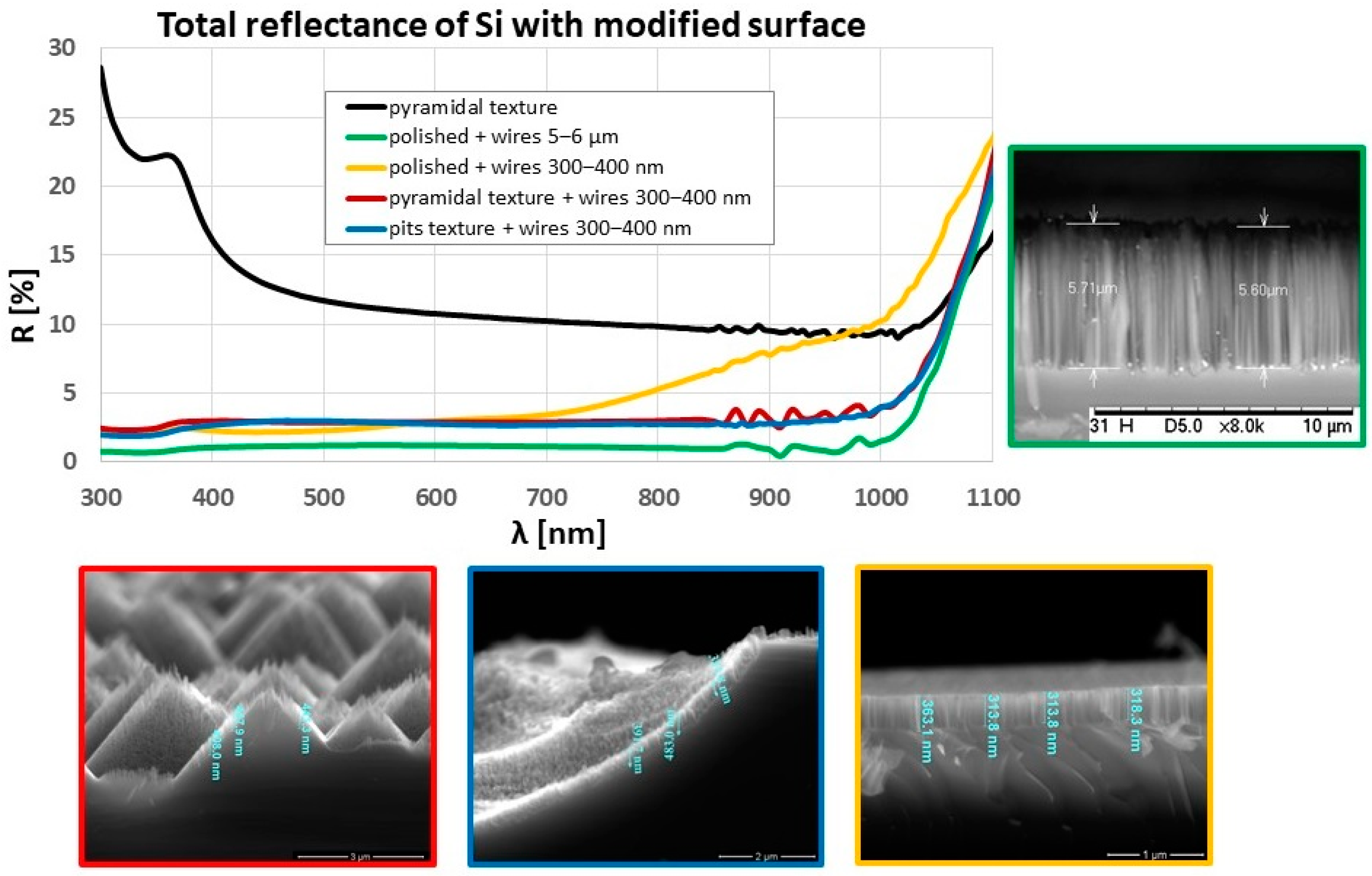
The motivation for the use of Si etched wires was a previous work in the field of effective texturing of silicon solar cells [
34]. Strong reduction in the total reflectance in the wavelength range of 300–1100 nm was critical to assume that this type of texture is predestined to act as a fully absorb material—‘black silicon’. Reflectance spectra are presented in
Figure 3.
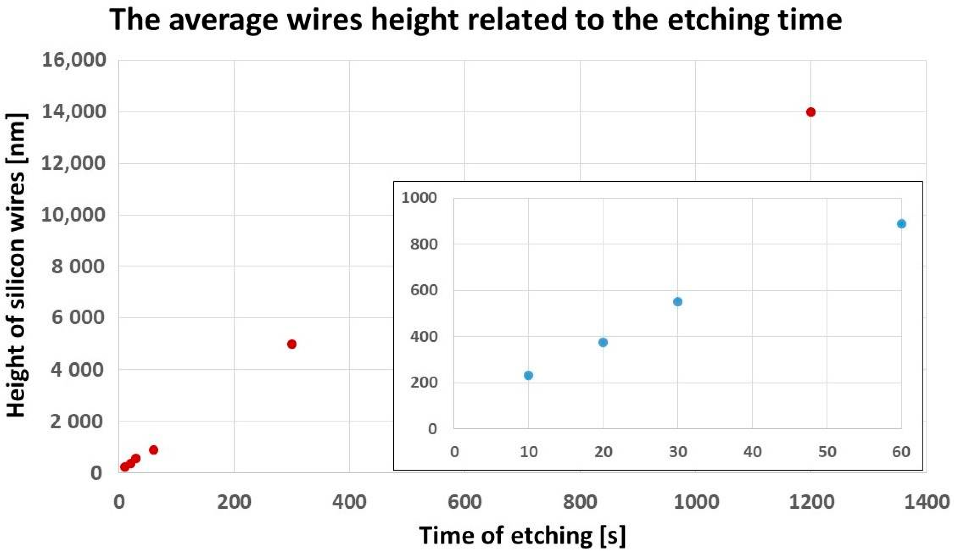
It is obvious that the height of the wires affects the roughness and development of the surface and therefore will consistently have a positive effect on the reduction in reflection. However, it should be remembered that the infinite porosity of the structure is impossible for two reasons: further processes of creating a silicon solar cell are hindered and the structure becomes brittle. Therefore, the height of the wires must be clearly defined and must be a compromise between maintaining good optical properties and porosity vs. the mechanical strength and the ability to carry out the processes of diffusion, passivation, applying thin layers, etc. [
36]. The average height related to the MAE etching time of the silicon wafer is listed in the
Table 1.
The data show that the etching of the wires and the resulting length is linearly proportional to the duration of etching, which is shown in
Figure 4.
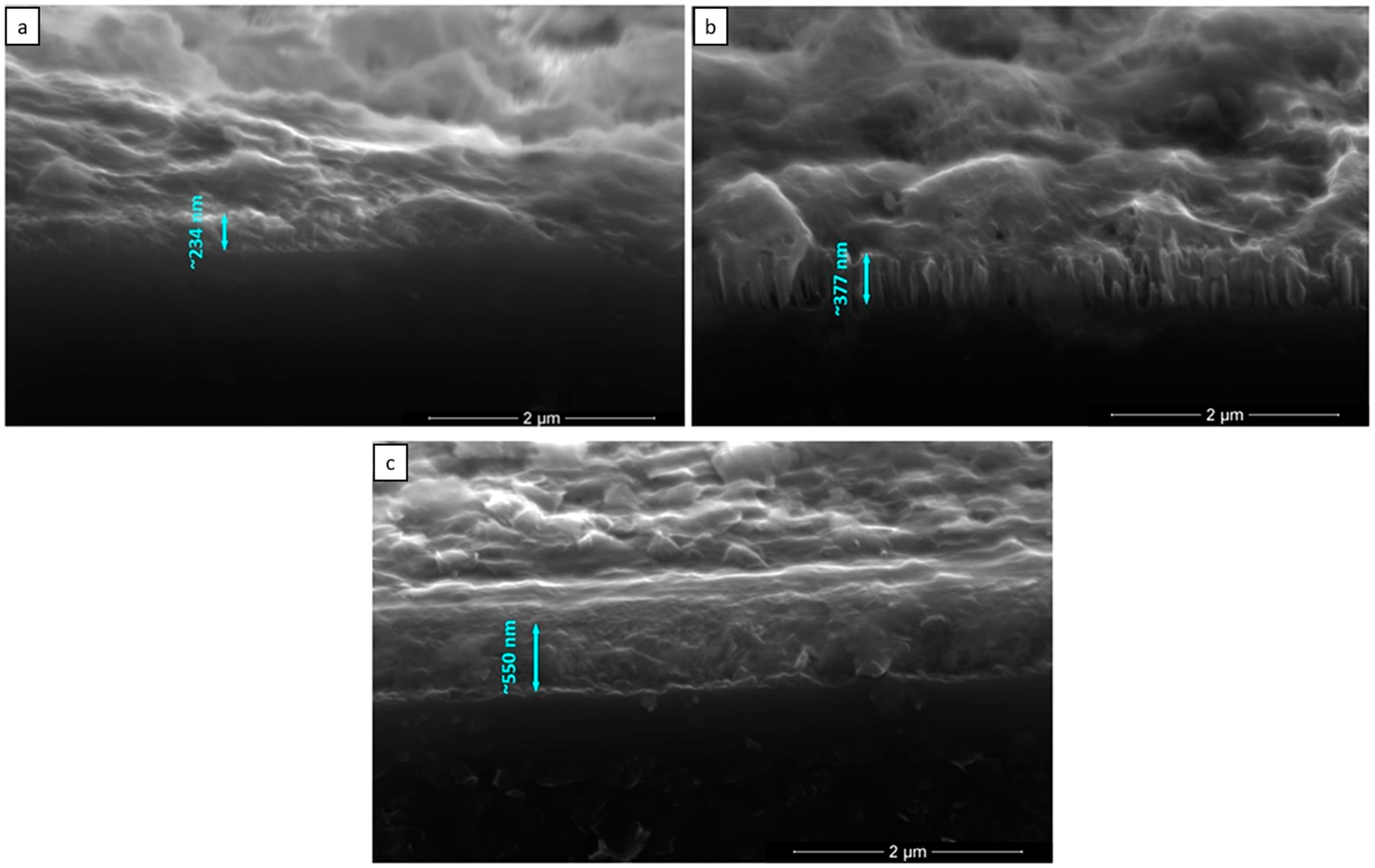
At this stage, due to the compromise described above, silicon wafers with wires up to 600 nm in length (i.e., with an etching time of up to 30 s) were accepted for testing. Ultimately, the best reflectance reduction was obtained for the hybrid-structured silicon sample (pyramids + wires or pits + wires), and this structure was the starting point for research involving the application of a dense layer of perovskite simultaneously filling the spaces between the wires.
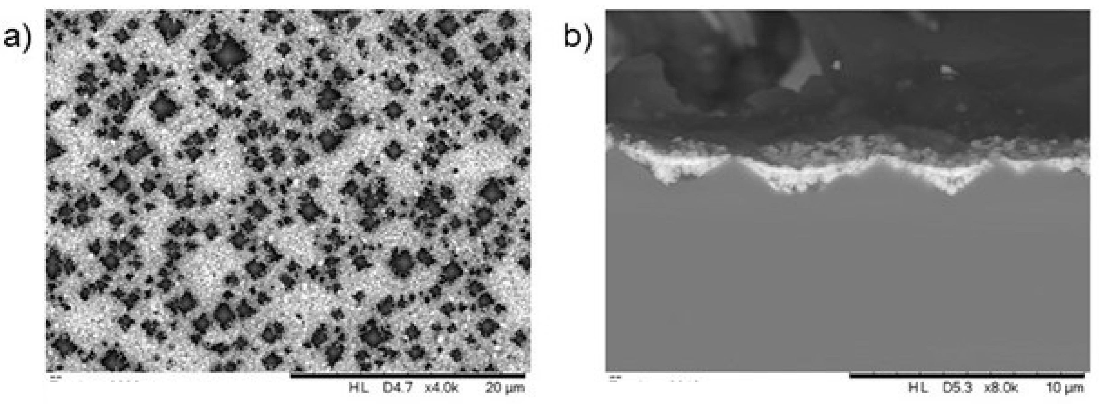
Figure 5 shows the resulting SEM image.
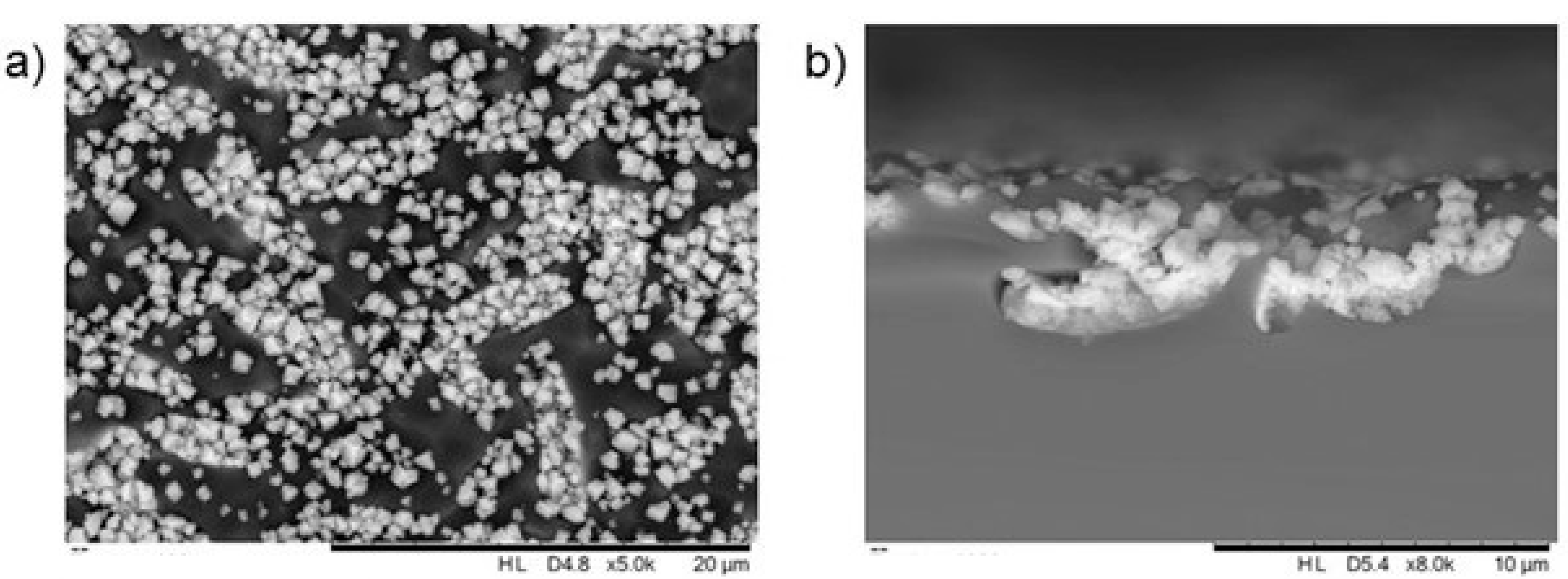
Figure 5 shows that the perovskite obtained in two-step processing, despite the scaffolding in the form of wires, did not fully cover the surface of the silicon wafer. The protruding tops of the pyramids were clearly visible including the previously etched wires. The result showed that the research should take a step back and determine whether the cause is the problem with applying the perovskite or the specificity of the texture with large dimensions reaching several microns (height of the pyramids). Therefore, attempts were made to deposit the perovskite in the same way on silicon wafers with a classic commercial texture. The application was carried out in two ways. Perovskite was applied to the two different samples: one etched in an alkaline solution, leading to the formation of pyramids, and the second etched in an acidic solution, leading to the formation of digestive pits (previously used for polycrystalline silicon). SEM images of the results are presented in
Figure 6 and
Figure 7.
The above images led the authors to conclude that the silicon texture above 1 micron is critical in coating the perovskite layer by the two-step method. At the moment, it seems that the proposed method of deposition is not possible to apply to such large structures. The authors are inclined to argue that other methods of perovskite deposition will be optimal, however, remaining in the spirit of simplicity and cost reduction, it was decided to further work on the two-step deposition of perovskite on silicon structures. In addition, literature reports and our own research showed that controlling the size of structures, especially in the case of a pyramidal texture, may allow for complete coverage with a perovskite absorber. Further research was limited to testing the last proposed structure indicated as a 1 in
Figure 2.
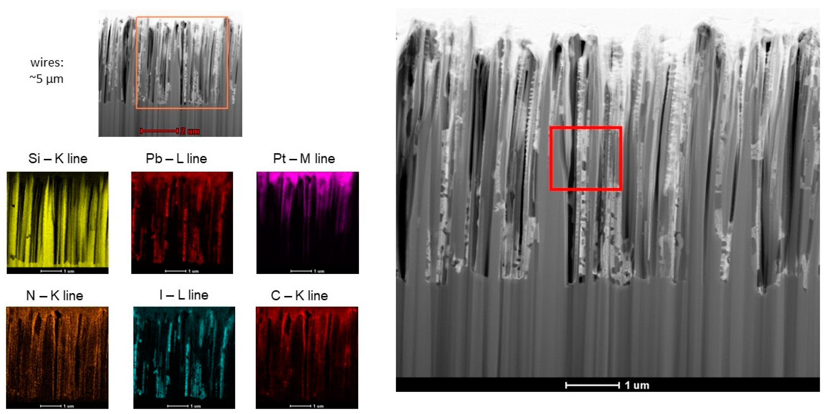
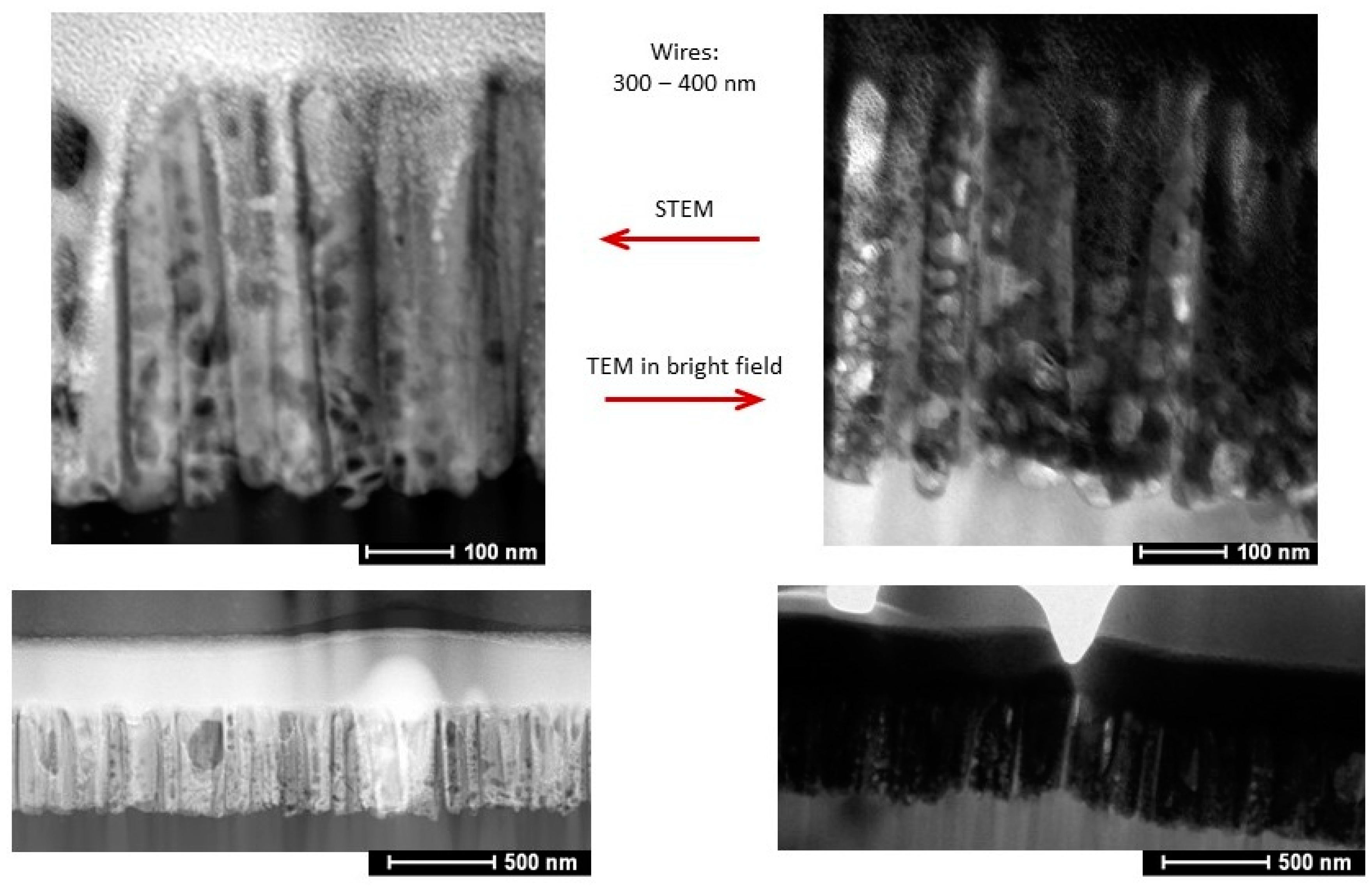
First, the perovskite was applied to relatively high wires with an average length of about 5 micrometers. The aim of this experiment was to check what penetration depth could be counted when applying perovskite by wet chemistry methods. TEM studies, presented in
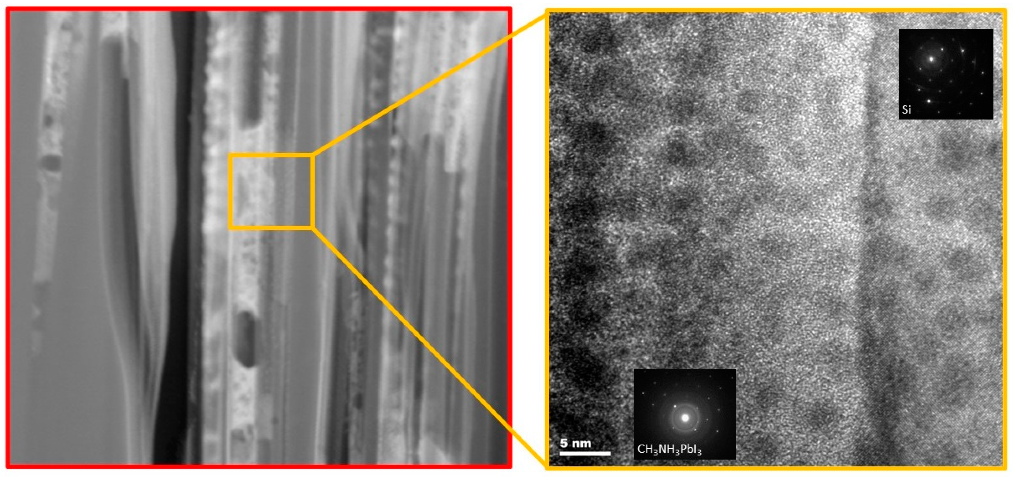
Figure 8, showed that the spaces between the wires were extensive, which makes it impossible to fully cover them and build up a capping layer. At the same time, determining the composition of elements shows that there is a clear separation boundary between silicon and perovskite. The precise determination of the transition zone of these two absorbers was performed using high-resolution transmission microscopy, which is shown in
Figure 9.
The combination of silicon and perovskite visible in the image is compact and continuous. No voids, air bubbles, and impurities were observed. The continuity of the crystal lattice of both silicon and perovskite was maintained. Thus, a natural step to maintain the continuity of the perovskite structure during spin-coating of PbI2 was to perform the same process on a less rough surface in this case and the lower wires. Here, three examples of 10, 20, and 30 s of etching time were chosen, resulting in the formation of wires with a length of up to 600 nm.
Considering that the two-stage process of perovskite deposition and ensuring the continuity of the layer on the porous substrate depends on the first stage-PbI
2 spin-coating because the second stage (i.e., immersion in MAI) will fully react with the previously applied lead iodide. The degree of surface coverage with perovskite of silicon nanowires is presented in
Figure 10.
The SEM images show that it is possible to cover silicon nanowires up to 600 nm in height with a continuous layer of perovskite using the two-step method based on wet chemistry. The presented perovskite layers are compact and in all samples fully fill the spaces between the wires and additionally create a capping layer.
For the selected sample (etched in 20 s and with a wire height of approx. 377 nm) shown in
Figure 10b, detailed studies were performed to confirm this assumption. The STEM and TEM BF examinations are shown in
Figure 11.
The STEM and TEM investigations confirmed the complete filling of the space between the wires and the presence of the perovskite layer. Both images clearly show that there is a limit to the structure porosity that can be homogeneously covered with wet chemistry methods.
4. Discussion
The conducted research was based on the microstructure analysis of silicon/perovskite transition zone as part of the Si/perovskite solar cell device preparation. Each change in a single element of the tandem can significantly affect the work of the entire device, therefore, the research must always be aimed at finally examining the optoelectronic properties of the structure as a whole. Unfortunately, the complexity of the problem resulting from the briefly described introduction does not allow us to investigate all of the interdisciplinary problems noticed above.
It is extremely important to select the absorber materials in a tandem solar cell. Silicon and perovskite appear to be ideally matched in terms of absorption ranges, which was also presented in the simulation part of this paper. In addition, the ability to control the energy gap in the perovskite allows for an increase in the efficiency of the entire TSC.
The authors would like to emphasize, that there are an infinite number of methods of the Si/perovskite tandem preparation. The selected methods tend to be simple, easily available, quick, and cheap. The aim of the research was to make a silicon/perovskite structure that would allow for further commercialization. It was decided to use wet chemistry methods: metal assisted etching (MAE) for silicon texturing and two-step deposition of a perovskite layer.
The polished silicon wafer, which is intentionally suitable for the application of perovskite by wet chemistry methods, unfortunately, leads to significant reflection losses. Therefore, as proposed in this paper, the structure of silicon with wires fulfils a double role: as a reflectance reducing texture and the scaffold for perovskite. Moreover, a compromise had to be found—maintaining good optical properties and porosity (as a scaffold) must be compared with the mechanical strength and the ability to carry out the processes of solar cell production. The optimal seems to be usage of a hybrid texture, which consists of elements of classic microstructure, reducing the reflection of light well known in classic solar cells based on crystalline silicon, additionally supported by the wire porosity at the level of individual hundreds of nanometers. Unfortunately, large sizes of structures resulting from classical texturization do not allow for continuous coverage with a perovskite layer using wet chemistry methods. However, it has been achieved, as shown in this paper, that it is possible to find such a structure of silicon wires, less than 600 nm in height, allowing for continuous coverage with a perovskite absorber and additional covering with a capping layer. At the same time, such a structure possesses high optical performance, which manifests itself in an excellent reflectance reduction in solar radiation. It was observed that the performed perovskite layer on silicon wires is continuous, compact, and free of air bubbles and contaminants. Additionally, as indicated in the literature [
2,
3,
5,
12], the front cell should be thick enough to absorb all photons with the energy above the bandgap in a single pass of light so the MAI is well suited for initial proof-of-concept tandem devices when the layer thickness is approximately 1 μm thick, which is still experimentally challenging while maintaining a high material quality.


 ,
, 


