
Application Properties of ZnO and AZO Thin Films Obtained by the ALD Method

 , , ,
, , ,
Abstract
:
1. Introduction
2. Materials and Methods
2.1. Sample Preparation
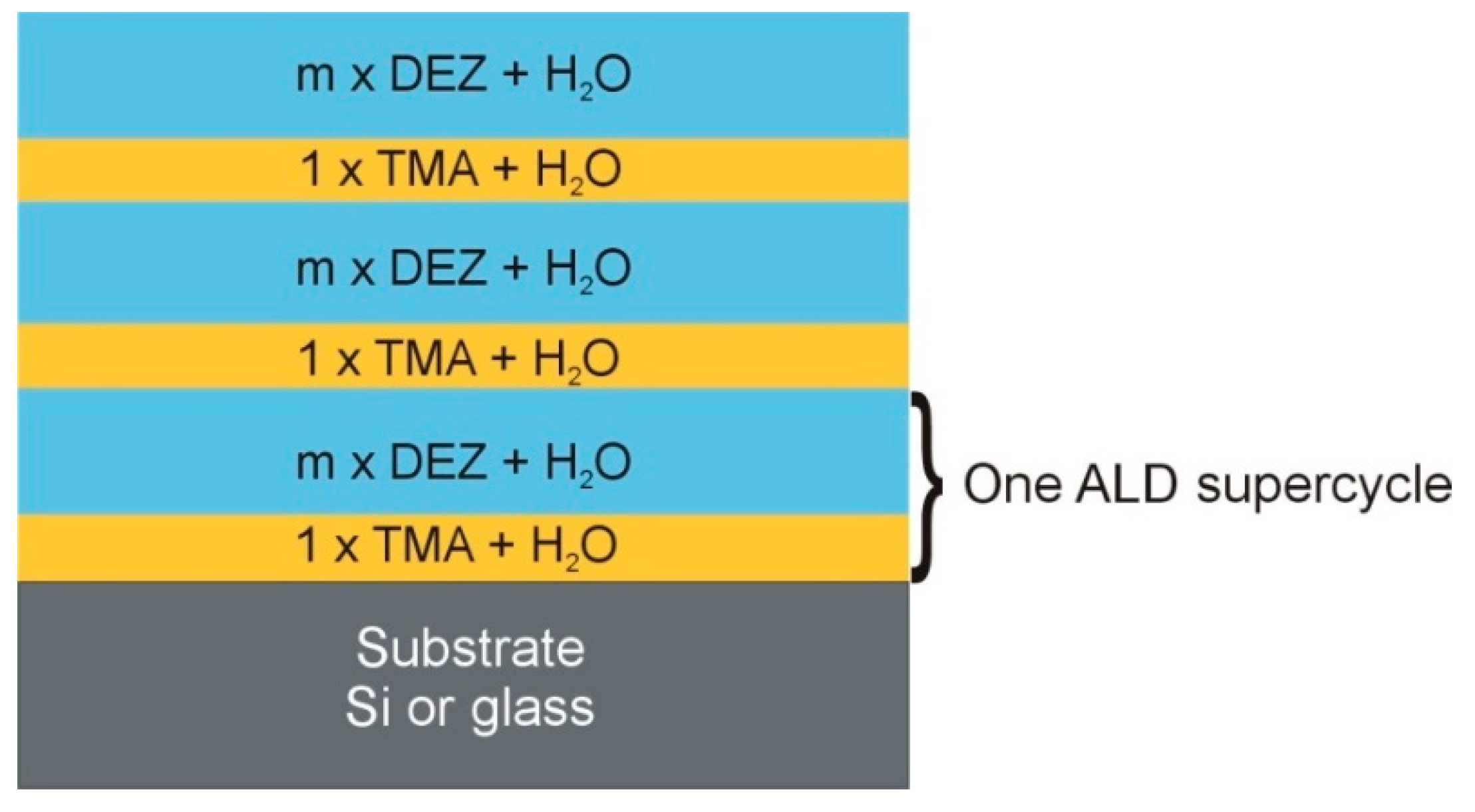
ALD Layer Deposition
2.2. Measurement Techniques
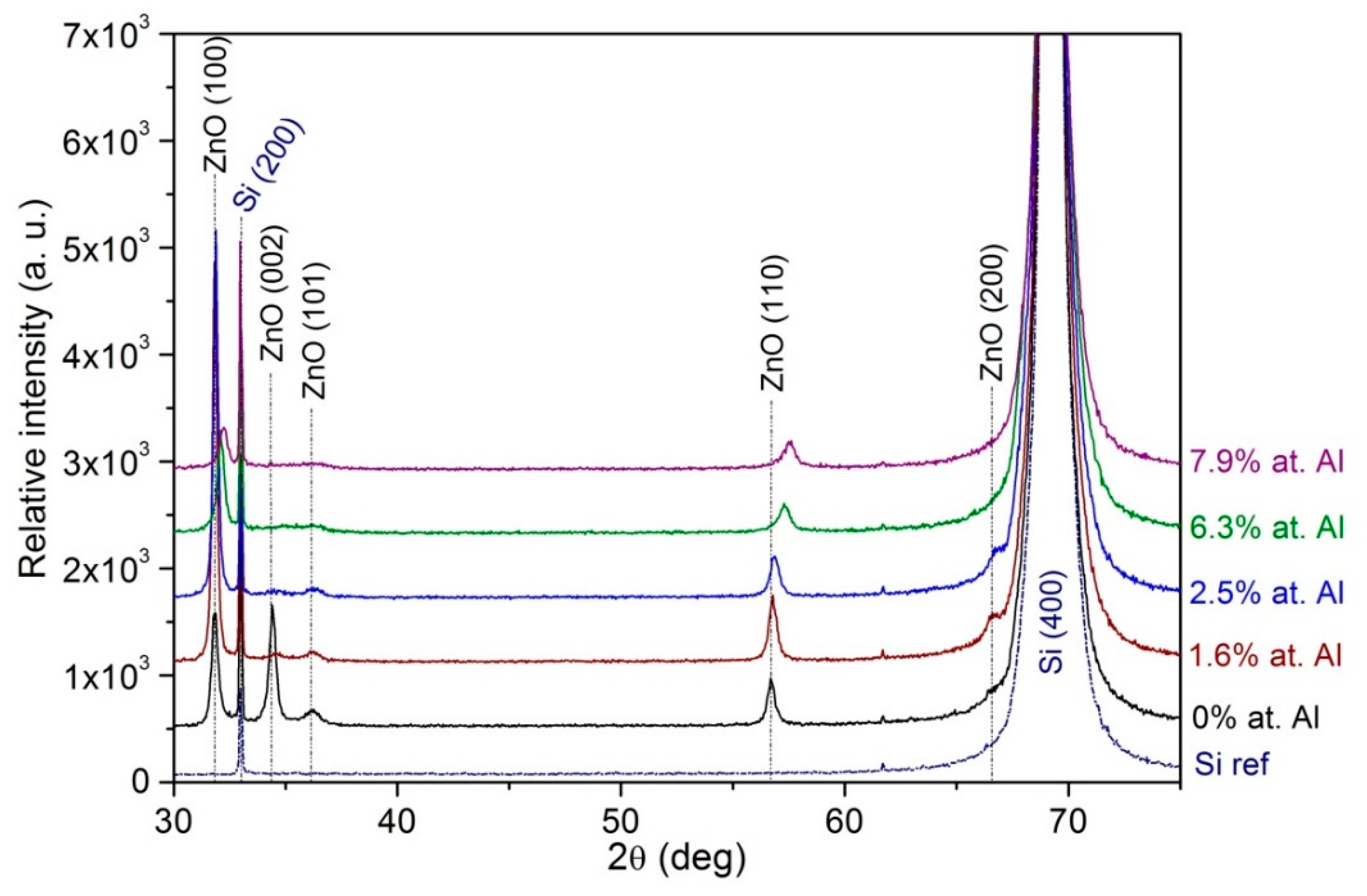
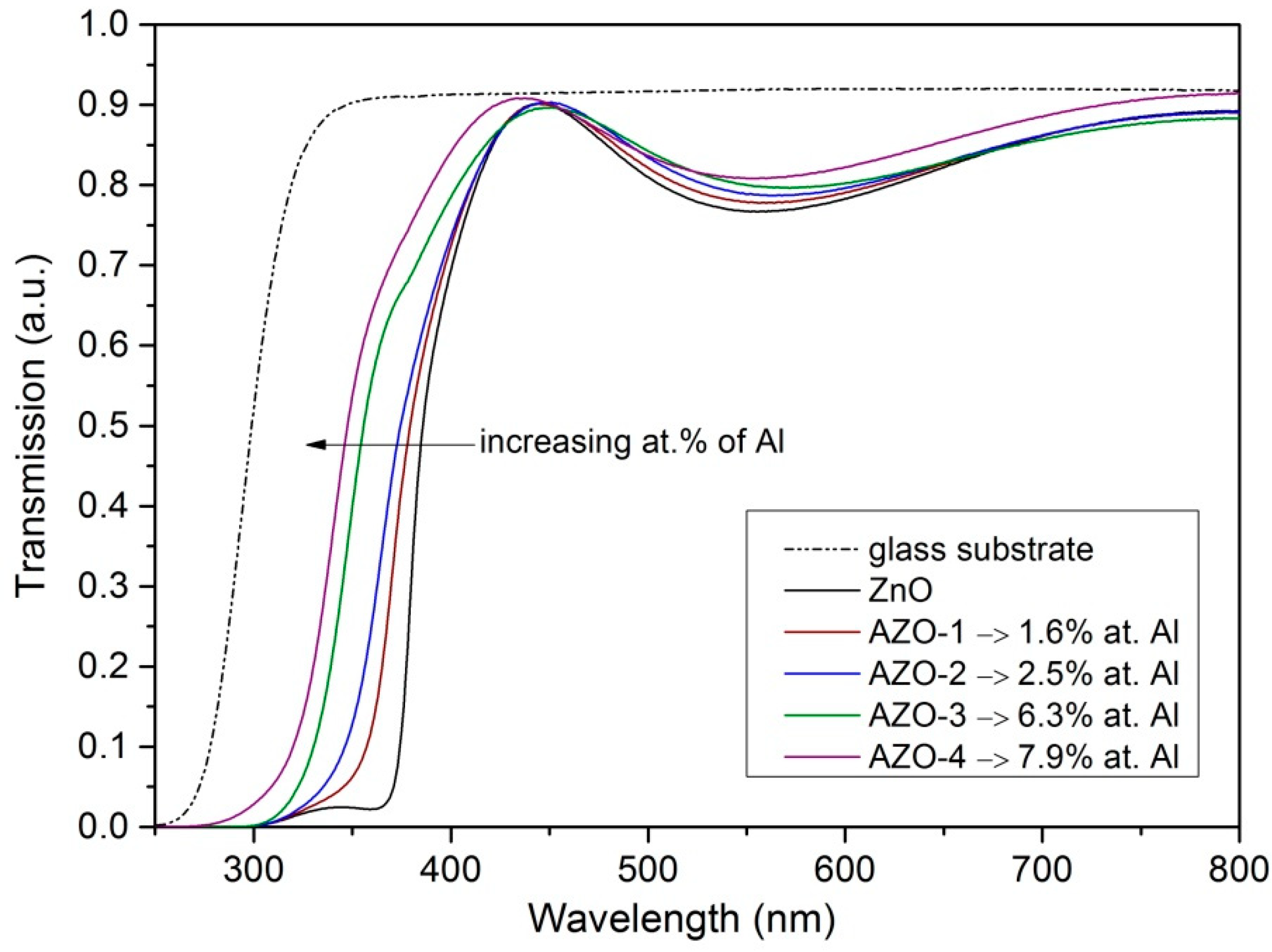
3. Results
4. Conclusions
Author Contributions
Funding
Institutional Review Board Statement
Informed Consent Statement
Conflicts of Interest
References
- Jagadish, C.; Pearton, S.J. (Eds.) Zinc Oxide Bulk, Thin Films and Nanostructures; Elsevier: Oxford, UK, 2006. [Google Scholar]
- Duenow, J.N.; Gessert, T.A.; Wood, D.M.; Barnes, T.M.; Young, M.; To, B.; Coutts, T.J. Transparent conducting zinc oxide thin films doped with aluminum and molybdenum. J. Vac. Sci. Technol. A 2007, 25, 955–960. [Google Scholar] [CrossRef]
- Minami, T.; Nanto, H.; Takata, S. Highly conductive and transparent aluminum doped zinc oxide thin films prepared by RF magnetron sputtering. Jpn. J. Appl. Phys. 1984, 23, L280–L282. [Google Scholar] [CrossRef]
- Minami, T. Transparent conducting oxide semiconductors fortransparent electrodes. Semicond. Sci. Technol. 2005, 20, S35. [Google Scholar] [CrossRef]
- Kim, H.; Gilmore, C.M.; Pique, A.; Horwitz, J.S.; Mattoussi, H.; Murata, H.; Kafafi, Z.H.; Chrisey, D.B. Electrical, optical, and structural properties of indium–tin–oxide thin films for organic light-emitting devices. J. Appl. Phys. 1999, 86, 6451–6461. [Google Scholar] [CrossRef]
- Coutts, T.J.; Young, D.L.; Li, X.; Mulligan, W.P.; Wu, X.J. Search for improved transparent conducting oxides: A fundamental investigation of CdO, Cd2SnO4, and Zn2SnO4. Vac. Sci. Technol. A 2000, 18, 2646. [Google Scholar] [CrossRef]
- Minami, T.; Suzuki, S.; Miyata, T. Transparent conducting impurity-co-doped ZnO:Al thin films prepared by magnetron sputtering. Thin Solid Films 2001, 53, 398–399. [Google Scholar] [CrossRef]
- Suzuki, A.; Matsushita, T.; Wada, N.; Sakamoto, Y.; Okuda, M. Transparent conducting Al-doped ZnO thin films prepared by pulsed laser deposition. Jpn. J. Appl. Phys. 1996, 35, L56. [Google Scholar] [CrossRef]
- Martin, A.; Espinos, J.P.; Justo, A.; Holgado, J.P.; Yubero, F.; Gonzalez-Elipe, A.R. Preparation of transparent and conductive Al-doped ZnO thin films by ECR plasma enhanced CVD. Surf. Coat. Technol. 2002, 289, 151–152. [Google Scholar] [CrossRef]
- Ohyama, M.; Kozuka, H.; Yoko, T.J. Sol-gel preparation of transparent and conductive aluminum-doped zinc oxide films with highly preferential crystal orientation. Am. Ceram. Soc. 1998, 81, 1622–1632. [Google Scholar] [CrossRef]
- Amakali, T.; Daniel, L.S.; Uahengo, V.; Dzade, N.Y.; de Leeuw, N.H. Structural and optical properties of ZnO thin films prepared by molecular precursor and sol–gel methods. Crystals 2020, 10, 132. [Google Scholar] [CrossRef] [Green Version]
- Bosio, A.; Romeo, N.; Mazzamuto, S.; Canevari, V. Polycrystalline CdTe thin films for photovoltaic applications. Prog. Cryst. Growth Charact. 2006, 52, 247–279. [Google Scholar] [CrossRef]
- Elmer, K. Resistivity of polycrystalline zinc oxide films: Current status and physical limit. J. Phys D Appl. Phys. 2001, 34, 3097–3108. [Google Scholar] [CrossRef]
- Pietruszka, R.; Witkowski, B.S.; Zielony, E.; Gwozdz, K.; Placzek-Popko, E.; Godlewski, M. ZnO/Si heterojunction solar cell fabricated by atomic layer deposition and hydrothermal methods. Sol. Energy 2017, 155, 1282–1288. [Google Scholar] [CrossRef]
- Kessler, J.; Bodegard, M.; Hedstrom, J.; Stolt, L. Baseline Cu(In, Ga)Se2 device production: Control and statistical significance. Sol. Energy Mater. Sol. Cells 2001, 67, 67–76. [Google Scholar] [CrossRef]
- Suntola, T. Atomic layer epitaxy. Mater. Sci. Rep. 1989, 4, 261–312. [Google Scholar] [CrossRef]
- Ritala, M.; Leskelä, M.; Dekker, J.-D.; Mutsaers, C.; Soininen, P.J.; Skarp, J. Perfectly conformal TiN and Al2O3 films deposited by atomic layer deposition. Chem. Vap. Depos. 1999, 5, 7–9. [Google Scholar] [CrossRef]
- Kukli, K.; Ritala, M.; Leskelä, M. Development of dielectric properties of niobium oxide, tantalum oxide, and aluminum oxide based nanolayered materials. J. Electrochem. Soc. 2001, 148, F35–F41. [Google Scholar] [CrossRef]
- Kopalko, K.; Godlewski, M.; Domagała, J.Z.; Łusakowska, E.; Minikayev, R.; Paszkowicz, W.; Szczerbakow, A. Monocrystalline ZnO films on GaN/Al2O3 by atomic layer epitaxy in gas flow. Chem. Mater. 2004, 16, 1447–1450. [Google Scholar] [CrossRef]
- Godlewski, M.; Guziewicz, E.; Szade, J.; Wójcik-Głodowska, A.; Krajewski, T.; Kopalko, K.; Jakieła, R.; Yatsunenko, S.; Przeździecka, E.; Kruszewski, P.; et al. Vertically stacked non-volatile memory devices–material considerations. Microelectron. Eng. 2008, 85, 2434–2438. [Google Scholar] [CrossRef]
- Puurunen, R.L. A short history of atomic layer deposition: Tuomo Suntola’s atomic layer epitaxy. Chem. Vap. Depos. 2014, 20, 332–344. [Google Scholar] [CrossRef] [Green Version]
- Godlewski, M.; Guziewicz, E.; Łuka, G.; Krajewski, T.; Łukasiewicz, M.; Wachnicki, Ł.; Wachnicka, A.; Kopalko, K.; Sarem, A.; Dalati, B. ZnO layers grown by atomic layer deposition: A new material for transparent conductive oxide. Thin Solid Films 2009, 518, 1145–1148. [Google Scholar] [CrossRef]
- Kowalik, I.A.; Guziewicz, E.; Kopalko, K.; Yatsunenko, S.; Wójcik-Głodowska, A.; Godlewski, M.; Dłużewski, P.; Łusakowska, E.; Paszkowicz, W. Structural and optical properties of low-temperature ZnO films grown by atomic layer deposition with diethylzinc and water precursors. J. Cryst. Growth 2009, 311, 1096–1101. [Google Scholar] [CrossRef]
- Guziewicz, E.; Godlewski, M.; Krajewski, T.; Wachnicki, Ł.; Szczepanik, A.; Kopalko, K.; Wójcik-Głodowska, A.; Przeździecka, E.; Paszkowicz, W.; Łusakowska, E.; et al. ZnO grown by atomic layer deposition: A material for transparent electronics and organic heterojunctions. J. Appl. Phys. 2009, 105, 122413. [Google Scholar] [CrossRef]
- Luka, G.; Krajewski, T.A.; Witkowski, B.S.; Wisz, G.; Virt, L.S.; Guziewicz, E.; Godlewski, M. Aluminum-doped zinc oxide films grown by atomic layer deposition for transparent electrode applications. J. Mater. Sci. Mater. Electron. 2011, 22, 1810–1815. [Google Scholar] [CrossRef] [Green Version]
- Luka, G.; Wachnicki, Ł.; Witkowski, B.S.; Krajewski, T.A.; Jakiela, R.; Guziewicz, E.; Godlewski, M. The uniformity of Al distribution in aluminum-doped zinc oxide films grown by atomic layer deposition. Mat. Sci. Eng. B-Adv. 2011, 176, 237–241. [Google Scholar] [CrossRef]
- Fujiwara, H. Spectroscopic Ellipsometry: Principles and Applications; John Wiley & Sons: Chichester, UK; Maruzen Co., Ltd.: Tokyo, Japan, 2007. [Google Scholar]
- Azzam, R.M.A.; Bashara, N.M. Ellipsometry and Polarized Light; North Holland Publishing Company: Amsterdam, The Netherlands, 1977; pp. 37–54. [Google Scholar]
- Woollam, J.A.; Johs, B.; Herzinger, C.M.; Hilfiker, J.; Synowicki, R.; Bungay, C.L. Overview of variable angle spectroscopic ellipsometry (VASE), part I: Basic theory and typical applications. Crit. Rev. 1999, CR72, 3–28. [Google Scholar] [CrossRef]
- J.A. Woollam Co., Inc. Complete Easy Data Analysis Manual; J.A. Woollam Co., Inc.: Lincoln, UK, 2008; pp. 18–22. [Google Scholar]
- Quemener, V.; Alnes, M.; Vines, L.; Rauwel, P.; Nilsen, O.; Fjellvag, H.; Monakhov, E.V.; Svensson, B.G. The work function of n-ZnO deduced from heterojunctions with Si prepared by ALD. J. Phys. D Appl. Phys. 2012, 45, 315101. [Google Scholar] [CrossRef]
- Banerjee, P.; Lee, W.-J.; Bae, K.-R.; Lee, S.B.; Rubloff, G.W. Structural, electrical, and optical properties of atomic layer deposition Al-doped ZnO films. J. Appl. Phys. 2010, 108, 043504. [Google Scholar] [CrossRef] [Green Version]
- Zhai, C.-H.; Zhang, R.-J.; Chen, X.; Zheng, Y.-X.; Wang, S.-Y.; Liu, J.; Dai, N.; Chen, L.-Y. Effects of Al doping on the properties of ZnO thin films deposited by atomic layer deposition. Nanoscale Res. Lett. 2016, 11, 1–8. [Google Scholar] [CrossRef] [PubMed] [Green Version]
- Scherrer, P. Bestimmung der inneren Struktur und der Größe von Kolloidteilchen mittels Röntgenstrahlen. Goettinger Nachr. 1918, 26, 98. [Google Scholar]
- Hsu, J.-C.; Chen, Y.-Y. Comparison of the optical and electrical properties of Al-Doped ZnO films using a lorentz model. Coatings 2019, 9, 4. [Google Scholar] [CrossRef] [Green Version]
- Hu, J.; Gordon, R.G. Textured aluminum-doped zinc oxide thin films from atmospheric pressure chemical-vapor deposition. J. Appl. Phys. 1992, 71, 880–889. [Google Scholar] [CrossRef]
- Aktaruzzaman, A.F.; Sharma, G.L.; Malhotra, L.K. Electrical, optical and annealing characteristics of ZnO:Al films prepared by spray pyrolysis. Thin Solid Films 1991, 198, 67–74. [Google Scholar] [CrossRef]
- Carter, C.B.; Norton, M.G. Ceramic Materials: Science and Engineering; Springer Science + Buisness Media: New York, NY, USA, 2013. [Google Scholar] [CrossRef]
- Willander, M.; Nur, O.; Sadaf, J.R.; Qadir, M.I.; Zaman, S.; Zainelabdin, A.; Bano, N.; Hussain, I. Luminescence from zinc oxide nanostructures and polymers and their hybrid devices. Materials 2010, 3, 2643–2667. [Google Scholar] [CrossRef]
- Wang, Q.J.; Wang, J.B.; Zhong, X.L.; Tan, Q.H.; Hu, Z.; Zhou, Y.C. Magnetism mechanism in ZnO and ZnO doped with nonmagnetic elements X (X = Li, Mg, and Al): A first-principles study. Appl. Phys. Lett. 2012, 100, 132407. [Google Scholar] [CrossRef]
- Li, Q.H.; Zhu, D.; Liu, W.; Liu, Y.; Ma, X.C. Optical properties of Al-doped ZnO thin films by ellipsometry. Appl. Surf. Sci. 2008, 254, 2922–2926. [Google Scholar] [CrossRef]
- Bouzourâa, M.-B.; Battie, Y.; Dalmasso, S.; Zaïbi, M.-A.; Oueslati, M.; En Naciri, A. Temperature dependent optical properties of ZnO thin film using ellipsometry and photoluminescence. Superlattices Microst. 2018, 117, 457–468. [Google Scholar] [CrossRef]
- Fricke, L.; Boentgen, T.; Lorbeer, J.; Bundesmann, C. An extended Drude model for the in-situ spectroscopic ellipsometry analysis of ZnO thin layers and surface modifications. Thin Solid Films 2014, 571, 437–441. [Google Scholar] [CrossRef]
- Pandey, S.K.; Awasthi, V.; Verma, S.; Gupta, M.; Mukherjee, S. Spetroscopic ellipsometry study on electrical and elemental properties of Sb-doped ZnO thin films. Curr. Appl. Phys. 2015, 15, 479–485. [Google Scholar] [CrossRef]
- Aghgonbad, M.M.; Sedghi, H. Influence of annealing temperature on optical properties of zinc oxide thin films analyzed by spectroscopic ellipsometry method. Chin. J. Phys. 2018, 56, 2129–2138. [Google Scholar] [CrossRef]
- Ferlauto, A.S.; Ferreira, G.M.; Pearce, J.M.; Wronski, C.R.; Collins, R.W. Analytical model for the optical functions of amorphous semiconductors from the near-infrared to ultraviolet: Applications in thin film photovoltaics. J. Appl. Phys. 2002, 92, 2424–2436. [Google Scholar] [CrossRef] [Green Version]
- Jellison, G.E.; Modine, F.A. Parameterization of the optical functions of amorphous materials in the interband region. Appl. Phys. Lett. 1996, 69, 371–373. [Google Scholar] [CrossRef]
- Tompkins, H.G.; Mc Gahan, W.A. Spectroscopic Ellipsometry and Reflectometry: A User’s Guide; John Wiley & Sons, Inc.: New York, NY, USA, 1999; p. 93. [Google Scholar]
- Liu, Y.C.; Hsieh, I.H.; Tung, S.K. Extraction of optical constants of zinc oxide thin films by ellipsometry with various models. Thin Solid Films 2006, 510, 32–38. [Google Scholar] [CrossRef]
- Xue, S.W.; Zu, X.T.; Zheng, W.G.; Deng, H.X.; Xiang, X. Effects of Al doping concentration on optical parameters of ZnO:Al thin films by sol gel technique. Phys. B Phys. Condens. Matter 2006, 381, 209–213. [Google Scholar] [CrossRef]
- Burstein, E. Anomalous optical absorption limit in InSb. Phys. Rev. 1954, 93, 632–633. [Google Scholar] [CrossRef]
- Jain, S.C.; McGregor, J.M.; Roulston, D.J. Band-gap narrowing in novel III-V semiconductors. J. Appl. Phys. 1990, 69, 3747. [Google Scholar] [CrossRef]
- Lu, J.G.; Fujita, S.; Kawaharamura, T.; Nishinaka, H.; Kamada, Y.; Ohshima, T.; Ye, Z.Z.; Zeng, Y.J.; Zhang, Y.Z.; Zhu, L.P.; et al. Carrier concentration dependence of band gap shift in n-type ZnO:Al films. J. Appl. Phys. 2007, 101, 083705. [Google Scholar] [CrossRef]


| Layer | Reagent | Pulse (s) | Purge (s) | Ratio of ALD Cycles |
|---|---|---|---|---|
| ZnO | DEZ | 0.04 | 1 | |
| H2O | 0.02 | 1 | ||
| AZO | TMA | 0.04 | 1 | 1:m (1 × TMA + H2O + m × DEZ + H2O) |
| H2O | 0.02 | 2 | ||
| DEZ | 0.04 | 1 | ||
| H2O | 0.02 | 1 |
| ZnO | AZO-1 | AZO-2 | AZO-3 | AZO-4 | |
|---|---|---|---|---|---|
| m | 0 | 29 | 19 | 9 | 7 |
| Al (%) | 0 | 1.6 | 2.5 | 6.3 | 7.9 |
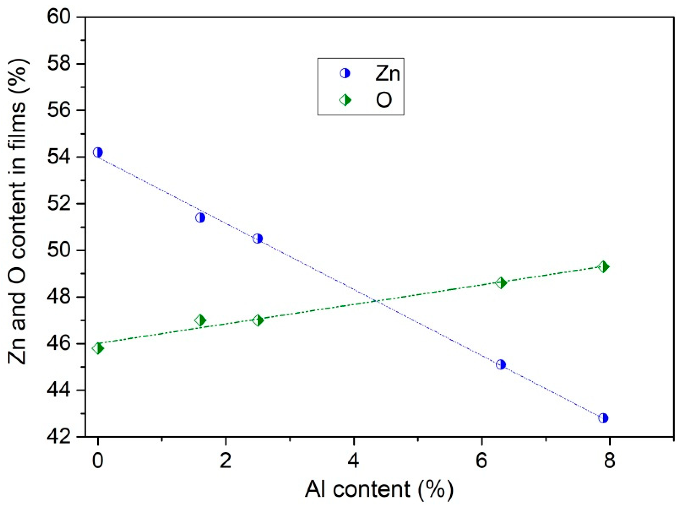
| Zn (%) | 54.2 | 51.4 | 50.5 | 45.1 | 42.8 |
| O (%) | 45.8 | 47.0 | 47.0 | 48.6 | 49.3 |
| Zn/O ratio | 1.19 | 1.09 | 1.07 | 0.93 | 0.87 |
| Al/Zn ratio | 0 | 0.03 | 0.05 | 0.14 | 0.18 |
| (Zn + Al)/O ratio | 1.19 | 1.13 | 1.13 | 1.06 | 1.03 |
| 1/m | - | 0.03 | 0.05 | 0.11 | 0.14 |
| ZnO | AZO-1 | AZO-2 | AZO-3 | AZO-4 | |
|---|---|---|---|---|---|
| ρ (Ωcm) | 4.93 × 10⁻² | 7.59 × 10⁻³ | 6.33 × 10⁻³ | 2.04 × 10⁻² | 9.98 × 10⁻² |
| μ (cm2/Vs) | 16.4 | 9.5 | 7.3 | 3.0 | 1.33 |
| n (cm−3) | 7.70 × 10¹⁸ | 8.66 × 10¹⁹ | 1.34 × 10²⁰ | 1.01 × 10²⁰ | 5.22 × 10¹⁹ |
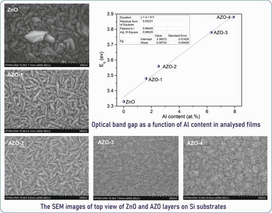
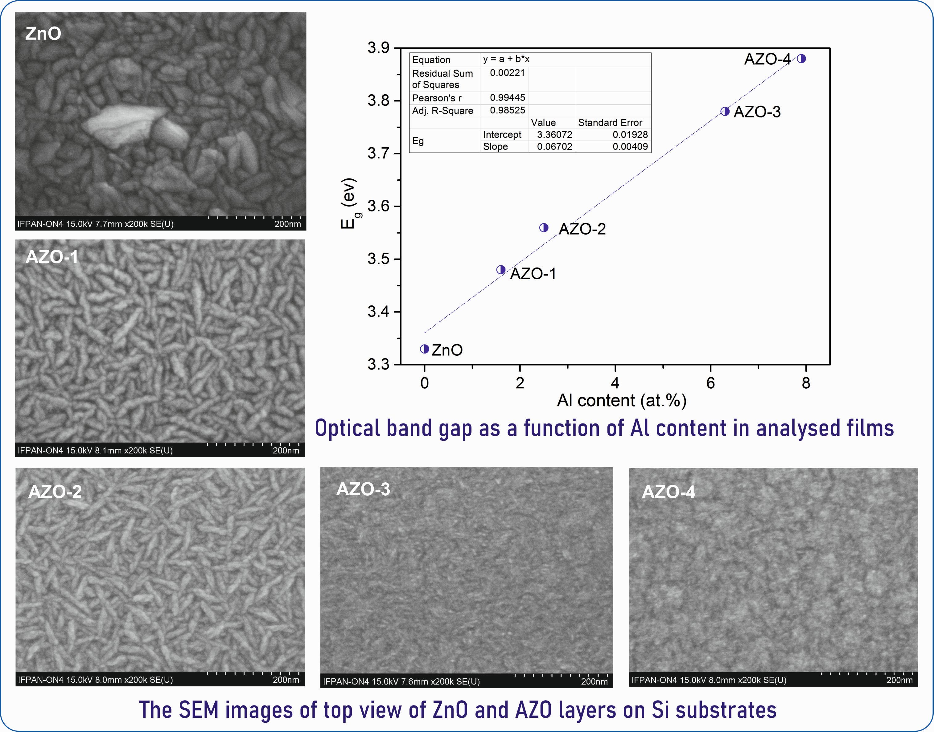
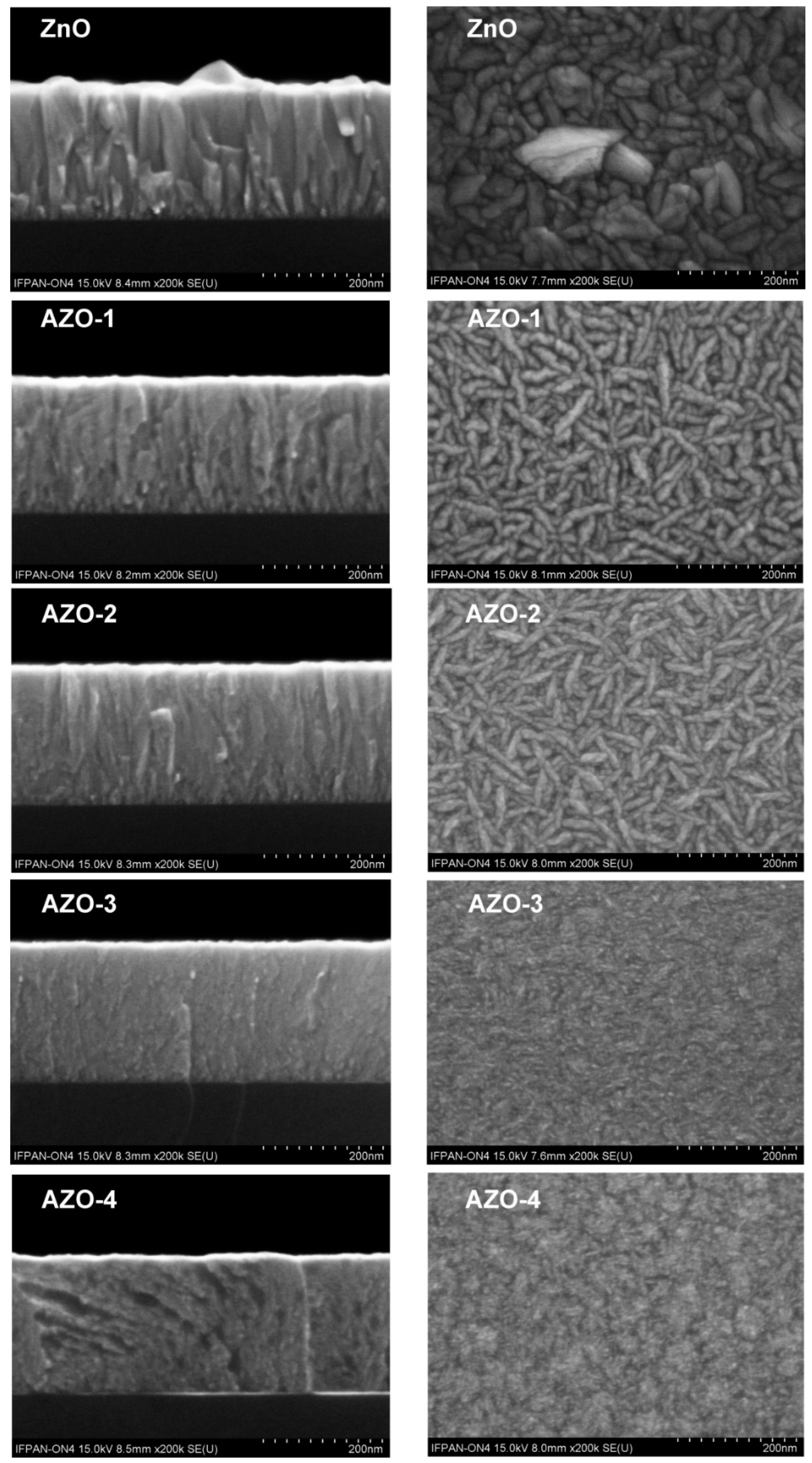
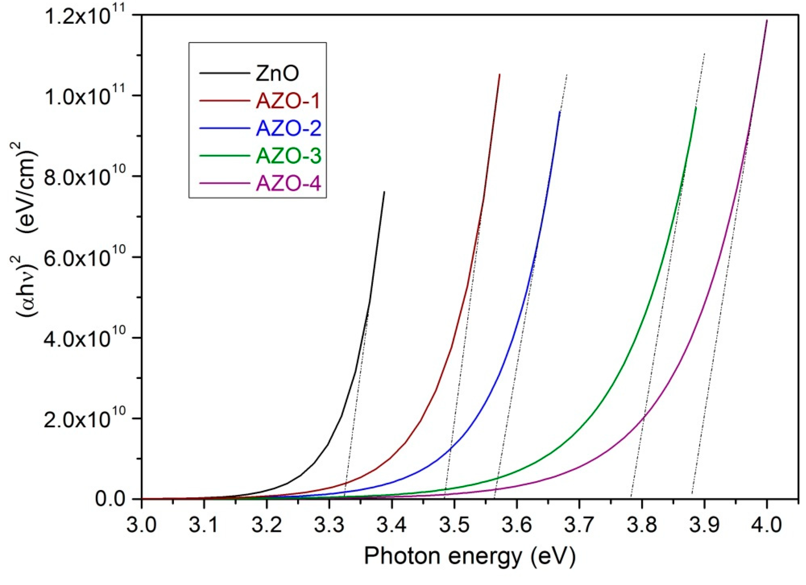
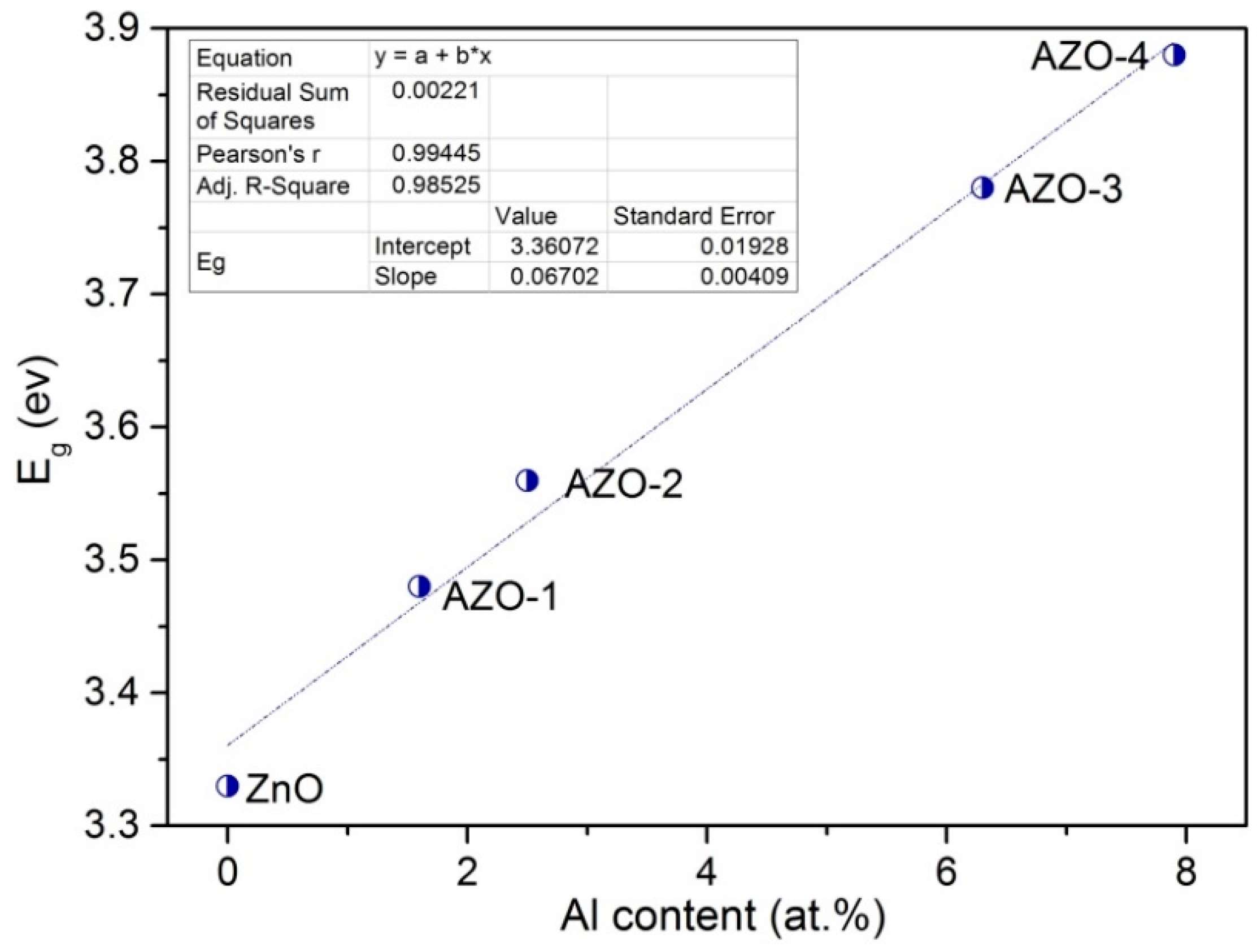
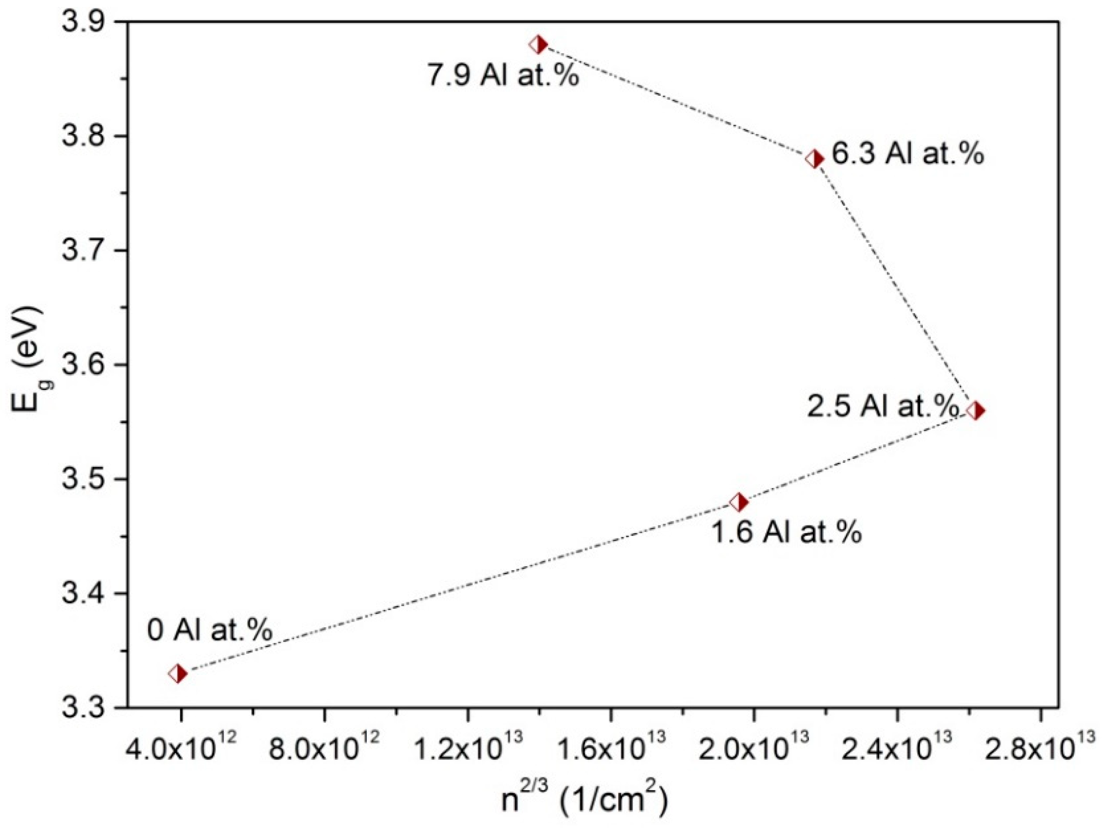
| Eg (eV) | 3.33 | 3.48 | 3.56 | 3.78 | 3.88 |
| Al Content (at.%) | Thickness from T–R (nm) | Thickness from SE (nm) | n from T–R for 600 nm | n from SE for 600 nm (on Base GO Model) | |
|---|---|---|---|---|---|
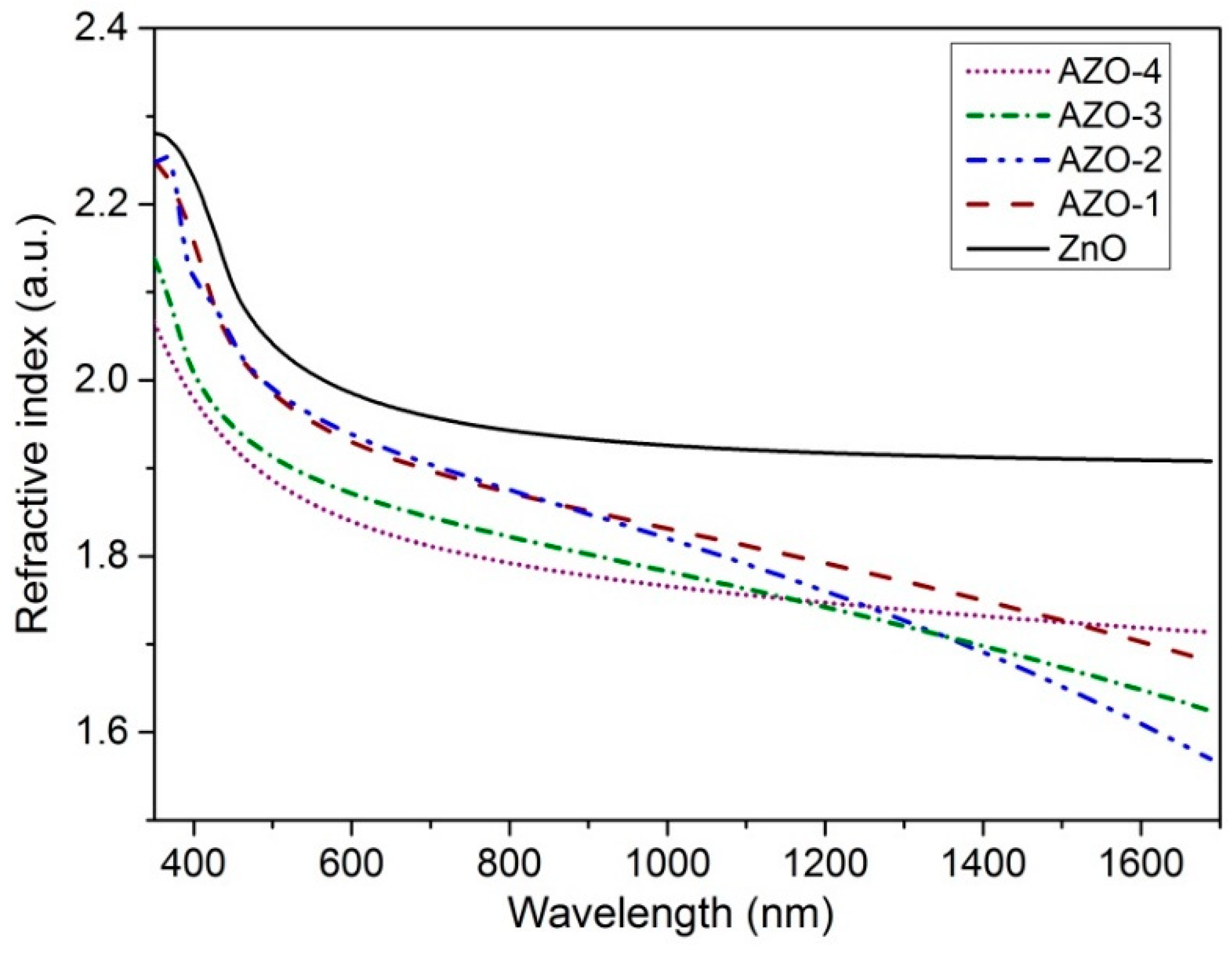
| ZnO | 0 | 214 | 214 | 2.01 | 1.98 |
| AZO-1 | 1.6 | 211 | 218 | 1.92 | 1.93 |
| AZO-2 | 2.5 | 213 | 220 | 1.94 | 1.92 |
| AZO-3 | 6.3 | 225 | 231 | 1.93 | 1.86 |
| AZO-4 | 7.9 | 228 | 233 | 1.85 | 1.81 |
Publisher’s Note: MDPI stays neutral with regard to jurisdictional claims in published maps and institutional affiliations. |
© 2021 by the authors. Licensee MDPI, Basel, Switzerland. This article is an open access article distributed under the terms and conditions of the Creative Commons Attribution (CC BY) license (https://creativecommons.org/licenses/by/4.0/).
Share and Cite
Swatowska, B.; Powroźnik, W.; Czternastek, H.; Lewińska, G.; Stapiński, T.; Pietruszka, R.; Witkowski, B.S.; Godlewski, M. Application Properties of ZnO and AZO Thin Films Obtained by the ALD Method. Energies 2021, 14, 6271. https://doi.org/10.3390/en14196271
Swatowska B, Powroźnik W, Czternastek H, Lewińska G, Stapiński T, Pietruszka R, Witkowski BS, Godlewski M. Application Properties of ZnO and AZO Thin Films Obtained by the ALD Method. Energies. 2021; 14(19):6271. https://doi.org/10.3390/en14196271
Chicago/Turabian StyleSwatowska, Barbara, Wiesław Powroźnik, Halina Czternastek, Gabriela Lewińska, Tomasz Stapiński, Rafał Pietruszka, Bartłomiej S. Witkowski, and Marek Godlewski. 2021. "Application Properties of ZnO and AZO Thin Films Obtained by the ALD Method" Energies 14, no. 19: 6271. https://doi.org/10.3390/en14196271