Review

On the Practical Evaluation of the Switching Loss in the Secondary Side Rectifiers of LLC Converters

by
Manuel Escudero
1,*,
Matteo-Alessandro Kutschak
1,
Francesco Pulsinelli
1,
Noel Rodriguez
2 and
Diego Pedro Morales
2
1
Infineon Technologies Austria AG, 9500 Villach, Austria
2
Department of Electronics and Computer Technology, University of Granada, 18011 Granada, Spain
*
Author to whom correspondence should be addressed.
Energies 2021, 14(18), 5915; https://doi.org/10.3390/en14185915
Submission received: 19 August 2021 / Revised: 14 September 2021 / Accepted: 16 September 2021 / Published: 17 September 2021

Abstract

:
The switching loss of the secondary side rectifiers in LLC resonant converters can have a noticeable impact on the overall efficiency of the complete power supply and constrain the upper limit of the optimum switching frequencies of the converter. Two are the main contributions to the switching loss in the secondary side rectifiers: on the one hand, the reverse recovery loss (Qrr), most noticeably while operating above the series resonant frequency; and on the other hand, the output capacitance (Coss) hysteresis loss, not previously reported elsewhere, but present in all the operating modes of the converter (under and above the series resonant frequency). In this paper, a new technique is proposed for the measurement of the switching losses in the rectifiers of the LLC and other isolated converters. Moreover, two new circuits are introduced for the isolation and measurement of the Coss hysteresis loss, which can be applied to both high-voltage and low-voltage semiconductor devices. Finally, the analysis is experimentally demonstrated, characterizing the switching loss of the rectifiers in a 3 kW LLC converter (410 V input to 50 V output). Furthermore, the Coss hysteresis loss of several high-voltage and low-voltage devices is experimentally verified in the newly proposed measurement circuits.

1. Introduction

A high-power off-line Power Supply Unit (PSU) normally comprises at least two stages: a front-end Power Factor Correction (PFC) and a back-end DCDC converter that provides isolation and a tight regulated output [1,2]. The total efficiency of the complete PSU is the result of multiplying the efficiency of each of the separate stages. Therefore, the total efficiency is always necessarily lower than the lowest of the individual efficiencies. This imposes very challenging requirements for the design of converters for the increasingly rising efficiency standards.
The main contributions to losses in the DCDC converter include the conduction, the auxiliary, the switching, the driving, and the core loss [3,4]. Most of these contributions to losses are, in some manner, frequency dependent, i.e., while the driving and the switching losses increase proportionally to the frequency, the core losses decrease proportionally to it (within the usable range of the specific material and considering a fixed geometry and number of turns, and therefore a decreasing magnitude of the magnetic field). The analysis of the conduction losses can be more complicated (depending on the construction of the conductors and the magnetics), but in all cases have a tendency to increase at the higher frequencies. Therefore, for every converter design there is an optimum switching frequency at which the overall sum of losses is at its minimum and the maximum efficiency is achieved.
Resonant and quasi-resonant converters aim to diminish or completely get rid of the switching loss contribution, i.e., soft-switching the power semiconductor devices. This can be accomplished by turning on at zero volts the so-called Zero Voltage Switching (ZVS) and turning off at zero current the so-called Zero Current Switching (ZCS) [5]. Among the resonant and quasi-resonant converters, the LLC has become very popular because of its simple circuitry (Figure 1) and the very high efficiencies it can achieve [6,7]. In the LLC the primary side devices are switched on in ZVS and can be switched off in ZCS, while the secondary side devices are switched on and off in ZVS, although they commutate with the transformer.
However, it has been reported that in the LLC (and other resonant converters), although the high-voltage (HV) primary side devices are soft-switched, their switching loss does not completely disappear [8]. The phenomenon can be interpreted as an equivalent series resistance (Ross) appearing in series to the output capacitance of the devices (Coss) during the resonant transitions [9,10,11,12,13,14,15,16]. However, there are no similar reports about the soft-switching loss contribution of the secondary side low-voltage (LV) rectifiers, even though the most mature technology for the LV secondary side rectifiers is the Silicon (Si) Trench MOSFET with shield-plate [17,18,19,20,21], and it is known that in their construction a series resistance appears with the output capacitance [22,23,24].
For the construction of a complete PSU targeting 97.5% peak efficiency, an LLC DCDC converter with the specifications in Table 1 was designed and built [25]. However, it was observed that the efficiency was unexpectedly decreasing while the series resonant frequency of the design was increasing (Figure 2). The origin of the unexpected contribution to losses was found to be the secondary side rectifiers, which was experimentally demonstrated with a new proposed technique for the characterization of the switching loss in the rectifiers of isolated converters. Moreover, the principle of the measurement technique was applied to a new testing circuit for the isolation and measurement of the Coss hysteresis loss (excluding Qrr contribution), which can be used for both HV and LV devices.
The rest of this document is organized as follows. In Section 2, the commutation of the secondary side rectifiers in LLC converters is analyzed and a new technique for the characterization of the switching loss (Qrr plus Coss hysteresis) within the application is proposed. In Section 3, two new circuits for the isolation of the Coss hysteresis loss are introduced and analyzed. The study is corroborated by the experimental results in Section 4 where the measurement techniques are applied to LV and to HV semiconductor devices. Finally, Section 5 presents a summary of conclusions of this work.

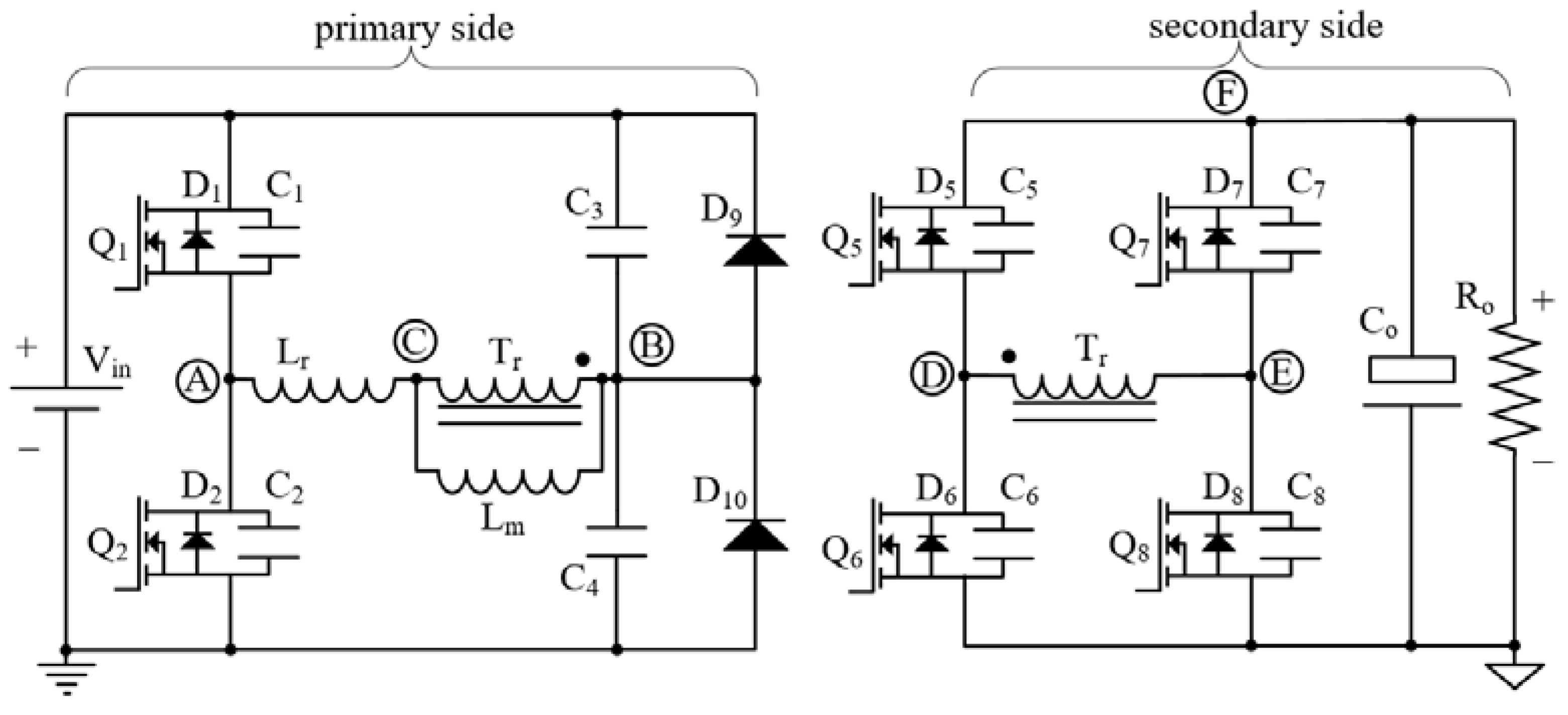
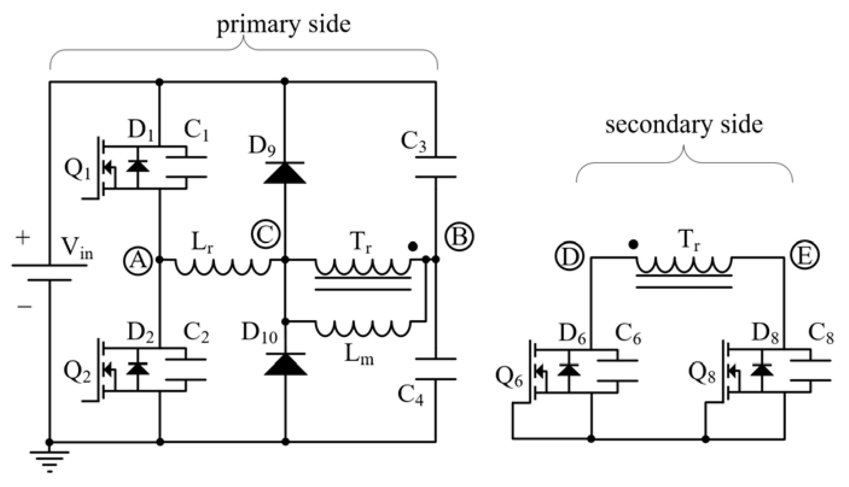
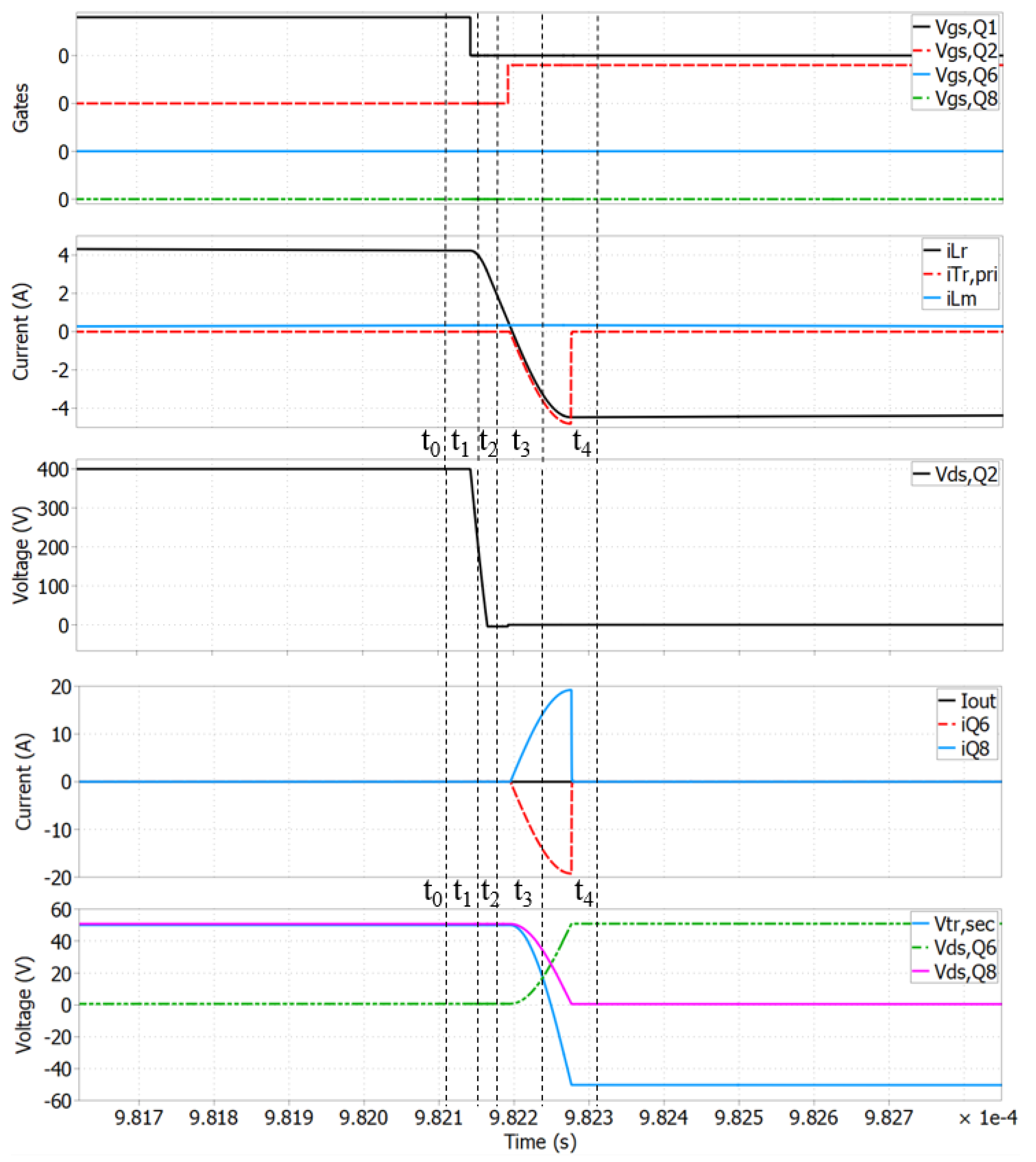
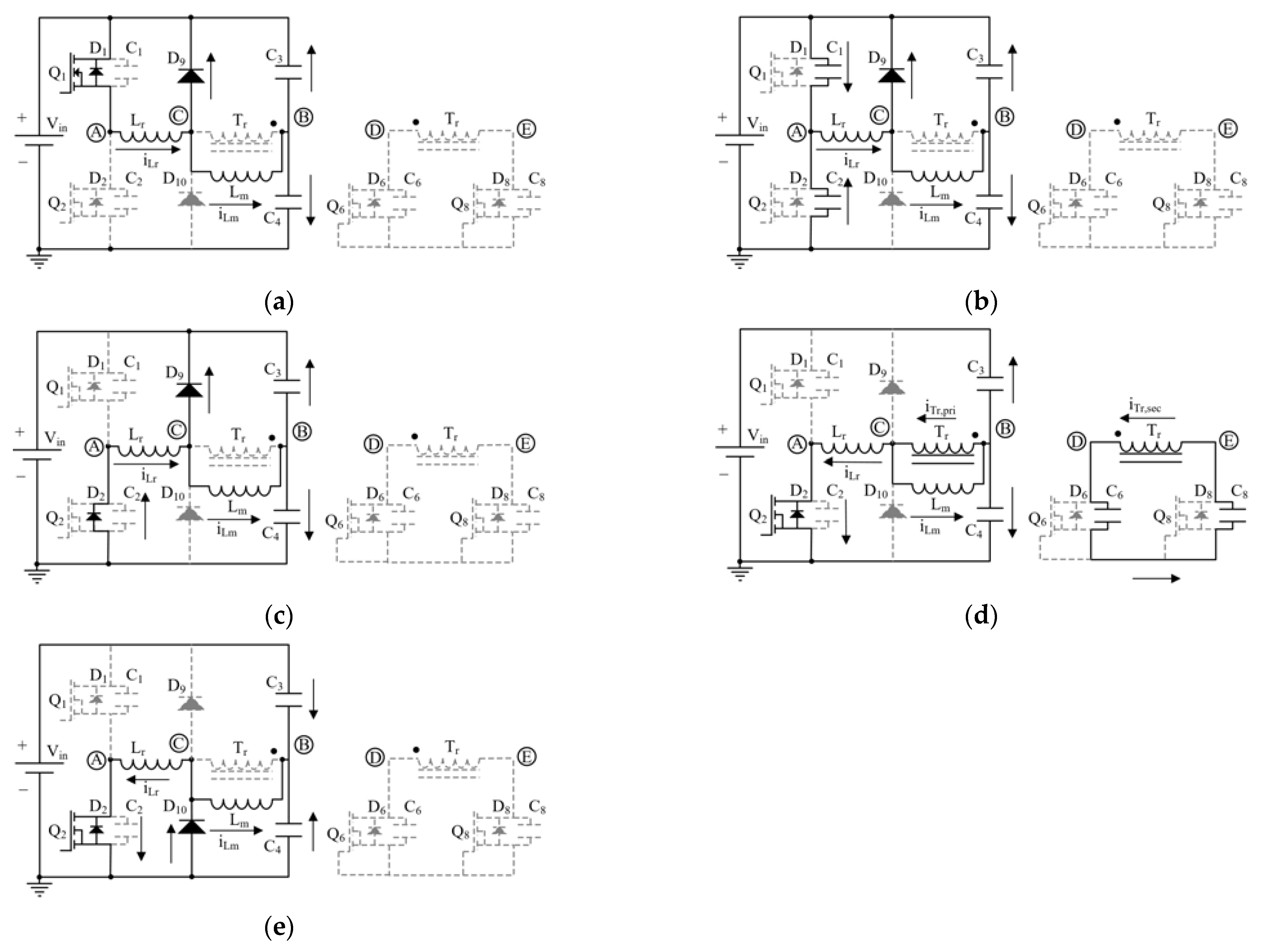
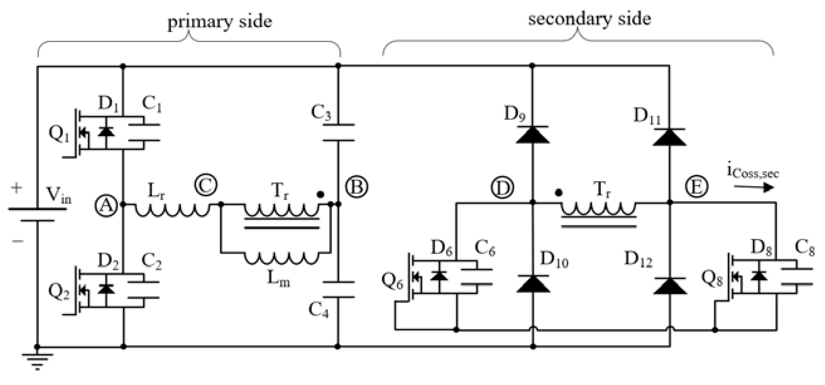
2. Analysis of the Commutation of the Rectifiers

The rectifiers in the LLC resonant converter can be switched on and off in ZVS. However, they are commutated by the transformer, with the di/dt being only limited by the series resonant inductor (Lr), the leakage of the transformer (Llkg) and other stray inductances. In this section, the commutation process is analyzed and a new technique is proposed for measuring Qoss, Qrr and the related switching loss.

2.1. Charge and Discharge of Coss
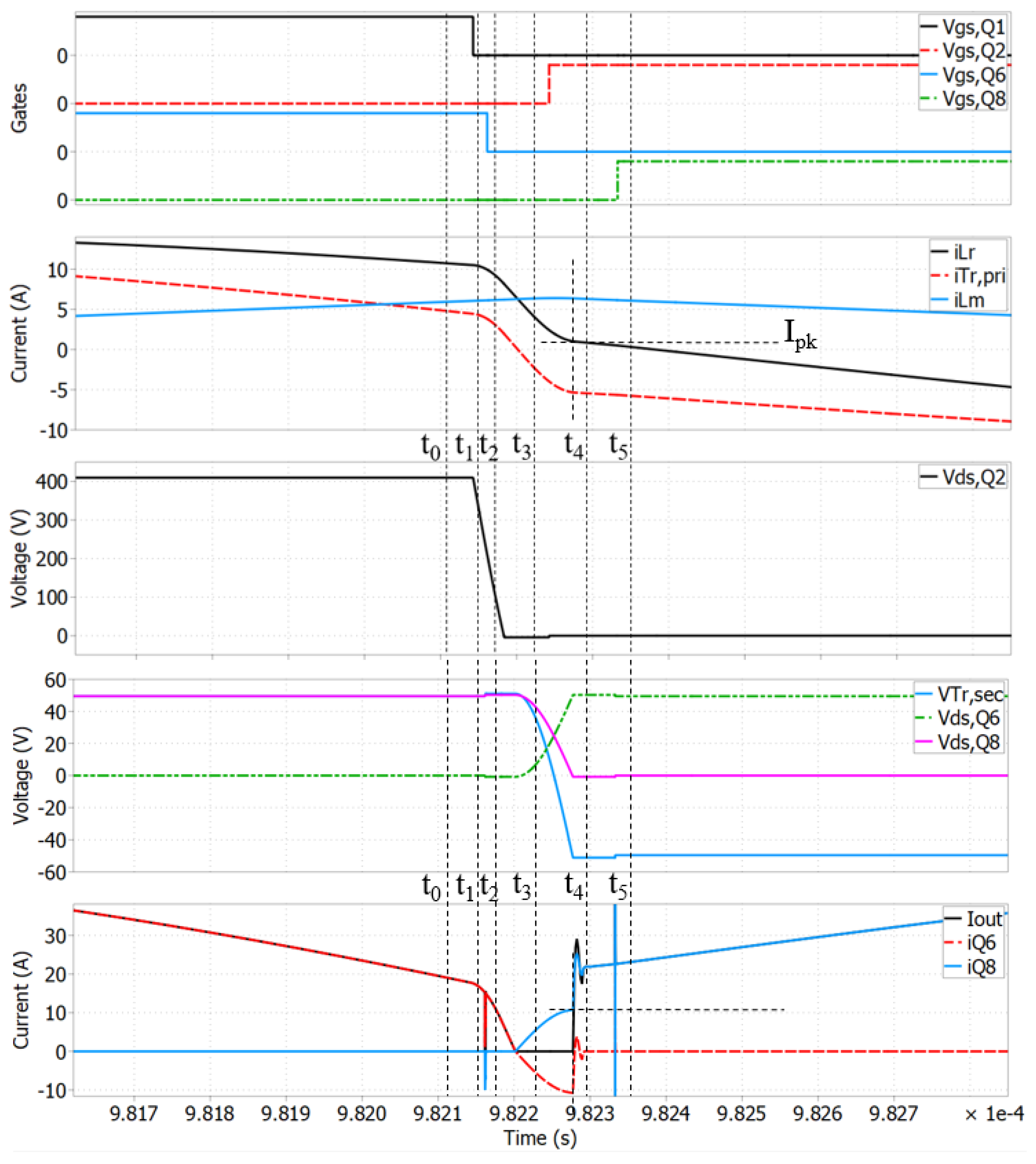
Figure 3 shows the main driving signals and waveforms in the LLC resonant converter during the commutation of the secondary side rectifiers. In this example, the converter is operating above the series resonant frequency, sometimes referred to as continuous conduction mode (CCM). Before the analysis, some assumptions are made: (1) all diodes and switches are ideal; (2) all switches are MOSFETs with intrinsic anti-parallel body diodes; (3) all capacitors and inductors are ideal; (4) C1 = C2, C5 = C6 = C7 = C8; (5) (C3 + C4) >> (C1 + C2); (6) Llkg = zero. In the following paragraphs, we analyze the operation principles of the rectifier’s commutation. It should be noted that the analyzed modes do not necessarily align with the rising of falling edges of the gate driving signals.
The primary high-side device Q1 is on and its channel is conducting. The current through Lr (iLr) flows towards the resonant capacitor Cr (C3 plus C4), which is therefore partially charged and discharged every period. The current iLr comprises the transformer-reflected load current (iTr,pri) and the magnetizing current (iLm), which both flow in the same direction at this point. Because of that, at higher loads and/or at lower frequencies the voltage excursion in Cr increases (also depending on the capacitor size).
In the secondary side of the converter, Q6 and Q7 are on and their channel is conducting the transformer secondary current (iTr,sec) that equals the output current (Iout) at this point.
2.
Mode 2[t1] (Figure 4b)
Both primary side devices are off and their capacitances C1 and C2 are being respectively charged and discharged by iLr, which continues to flow towards Cr, but starts to decrease with a slope that depends on the size of the capacitors C1 and C2 (natural resonance with Lr), and the voltage of Cr and Tr (i.e., the voltage effectively applied over Lr). Therefore, at higher loads, the current slope increases.
3.
Mode 3[t2] (Figure 4c)
Q6 and Q7 are turned off, and their intrinsic body diodes continue to conduct the secondary side current (iTr,sec). A transient drop in the current of iQ6 can be observed in Figure 3 due to the charge of C6 to –Vf and C8 to Vout plus Vf, corresponding to the forward voltage of their intrinsic antiparallel diode. It should be noted that in this example, the full transition of C1 and C2 from the upper voltage rail (Vin) to the lower voltage rail (GND) happens before the secondary side starts to commutate because C1 and C2 are relatively small size capacitors, and the turn-off current is relatively high. However, in other cases, the voltage transition of C1 and C2 can also overlap the commutation of the secondary side rectifiers [26].
4.
Mode 4[t3] (Figure 4d)
The voltage transition of C1 and C2 reaches under the GND rail and the intrinsic body D2 continues conducting the resonant current (iLr). The secondary side devices are all off. The output capacitances of Q6 and Q7 are being charged while the output capacitances of Q5 and Q8 are being discharged. It should be noted that during the charge of C6 and C7 and the discharge of C5 and C8, no current is being delivered to the output.
5.
Mode 5[t4] (Figure 4e)
The primary low-side device Q2 is on and the resonant current iLr flows mostly through its channel (although some current can be shared with its antiparallel diode). The diodes of the secondary side devices D5 and D8 conduct the secondary side current iTr,sec which is again equal to the output current Iout.
The peak current of the charge-discharge (Ipk) depends on the size of the capacitances C5–C8, the size of the series resonant inductor Lr (natural resonance), and the voltage excursion of the primary side resonant capacitor Cr (i.e., effectively higher voltage applied to Lr). Therefore, at higher loads Ipk and the dv/dt of the secondary side rectifiers increases.
6.
Mode 6[t5] (Figure 4f)
Q5 and Q8 are on and their channels are conducting the transformer secondary side current (iTr,sec). The primary reflected load current (iTr,pri) is larger than the magnetizing current (iLm) and of the opposite direction. Therefore, iLr flows at this point towards Q2.
It follows from the previous analysis that due to the charge and discharge of the secondary side rectifiers’ capacitance, the output current does not start at zero but at Ipk. This has several consequences:
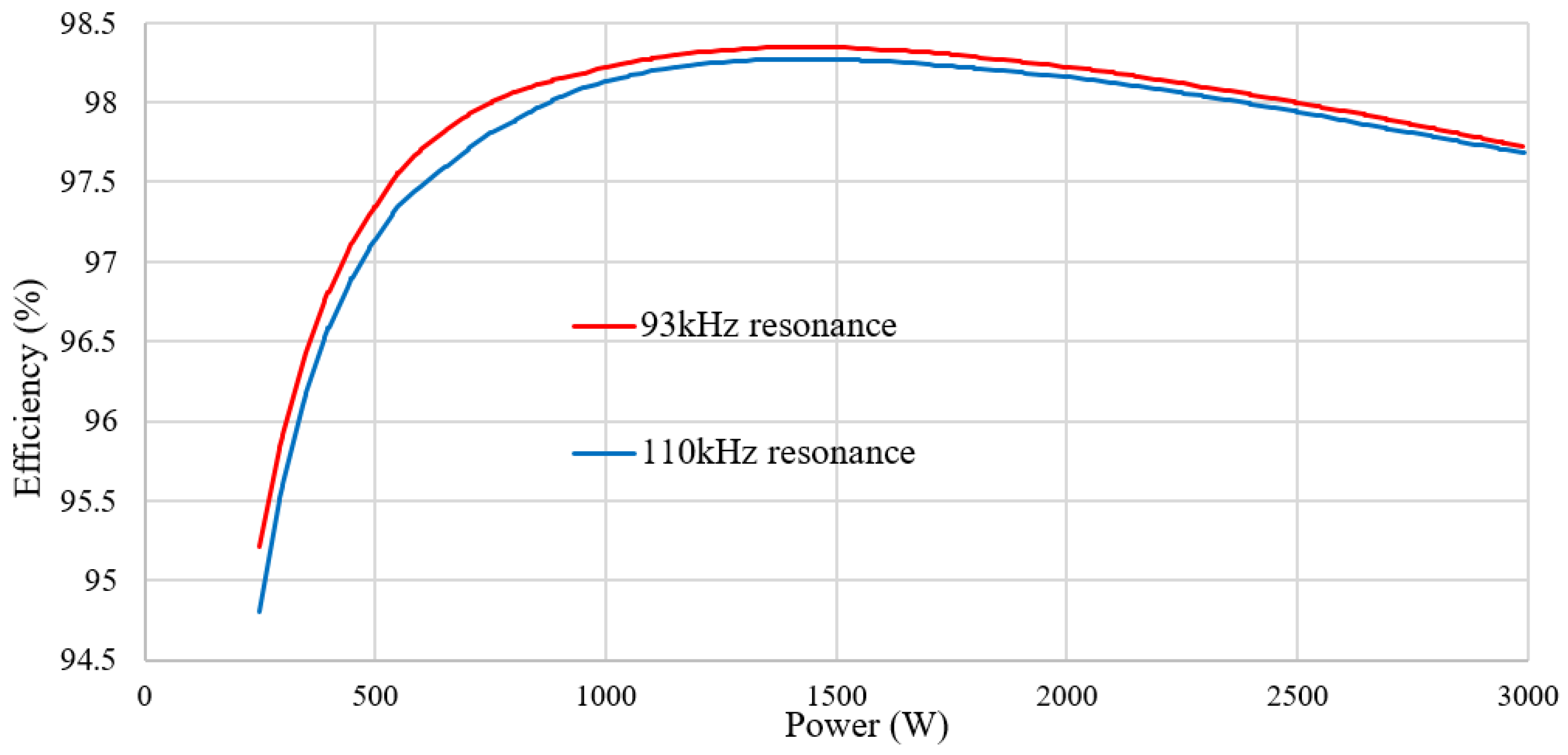
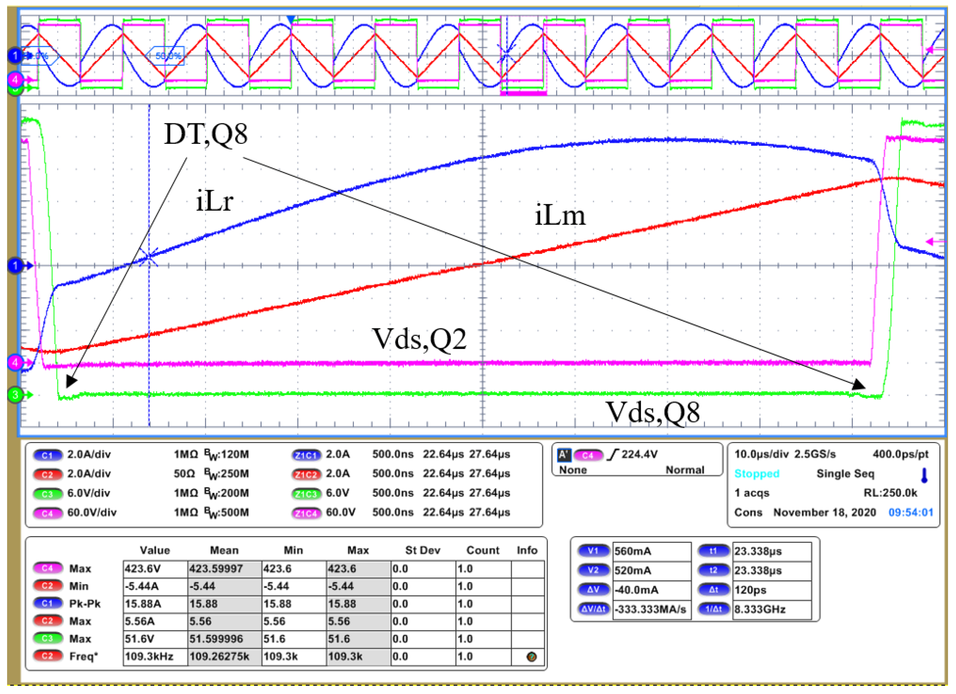
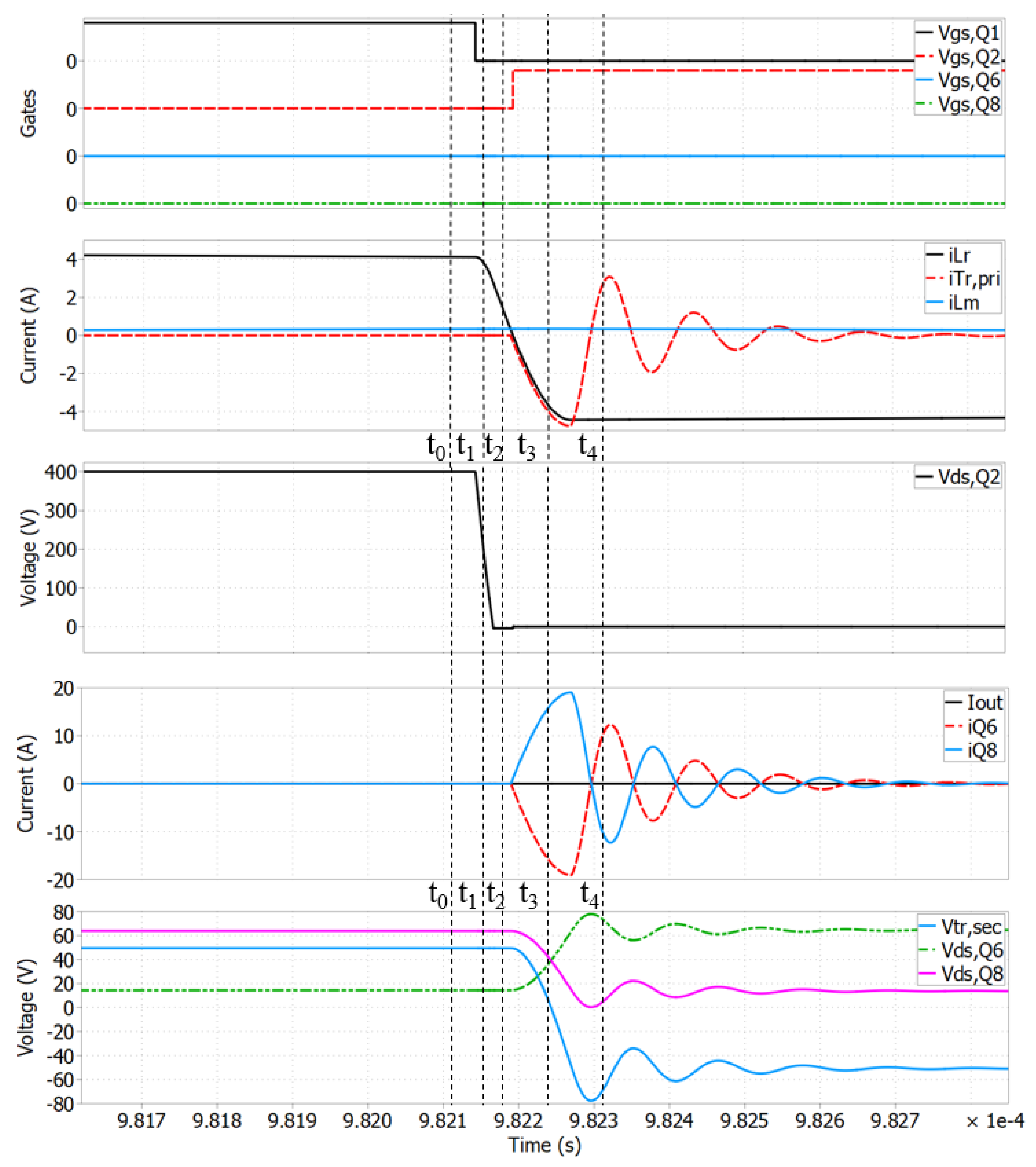
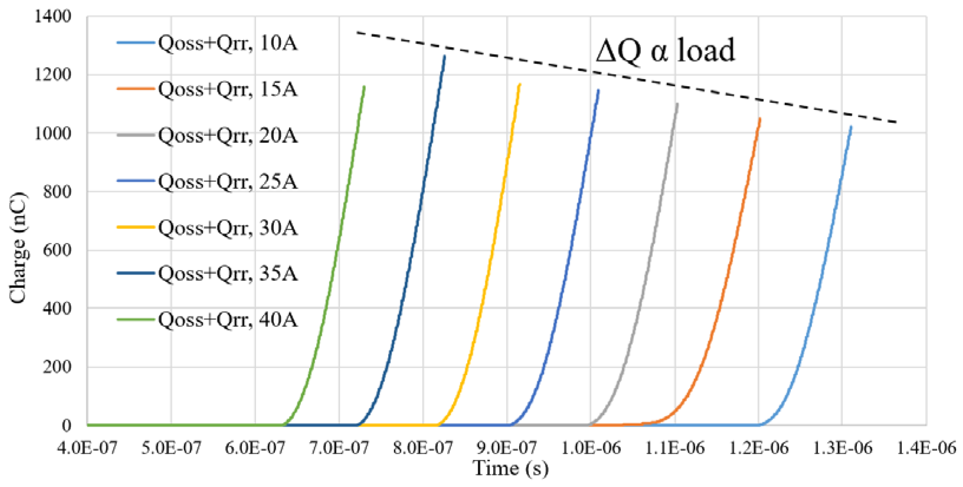
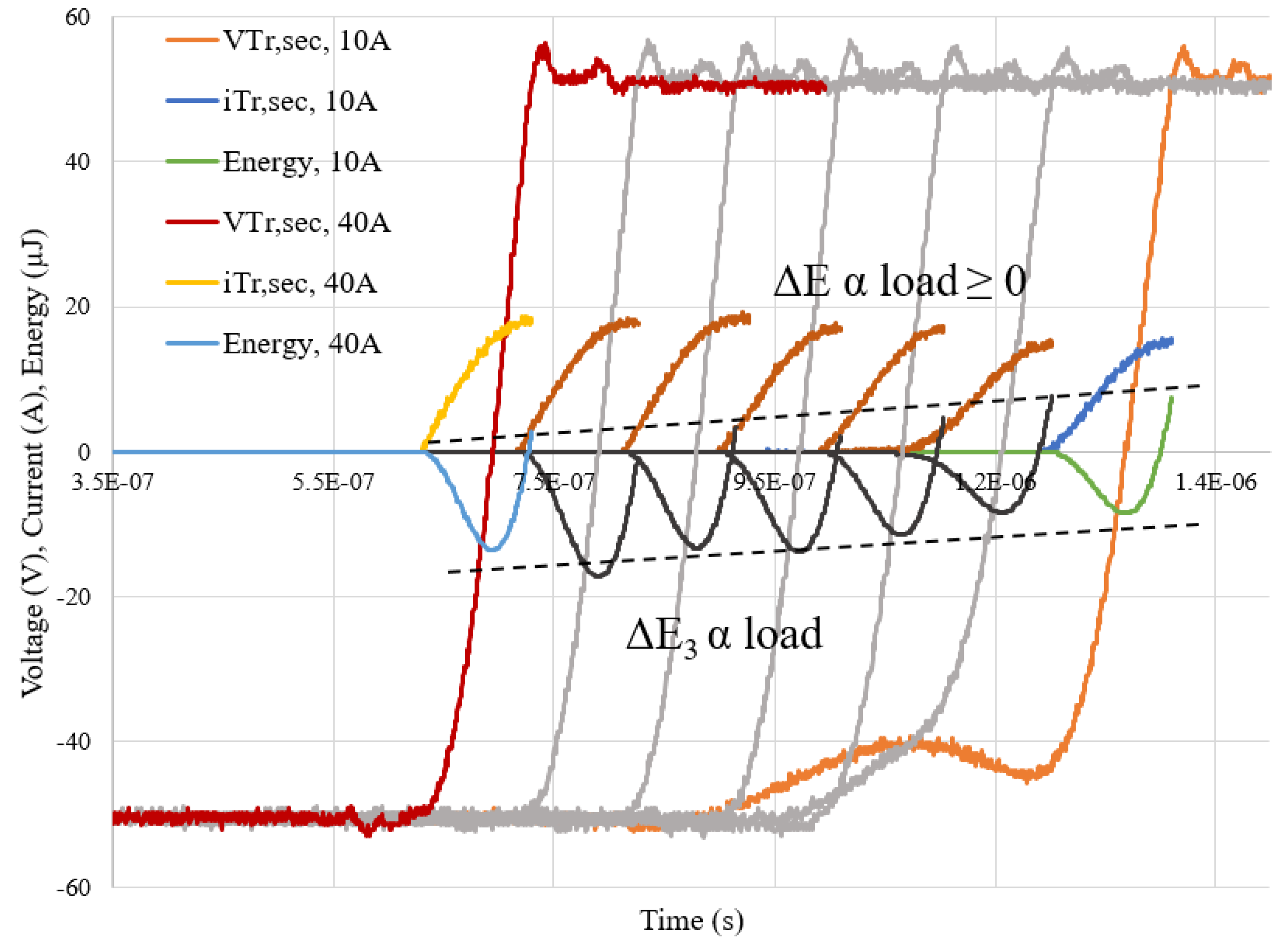
  • The natural resonance of Lr and Cr does not start at zero degrees, but it is shifted by an angle which depends on the ratio of Ipk with regard to the amplitude of the series resonance current (AIout) (1). However, AIout decreases in turn because of the Ipk shift, therefore effectively reducing the rms currents through the converter. Therefore, discontinuous conduction mode (DCM) operation can be observed above the series resonant frequency (Figure 5).
= arcsin ( I pk AI out )
  • During the charge and discharge of the rectifiers’ capacitance no current is being delivered to the output (so-called dead time), effectively increasing the output rms current. This effect is further described in [27].
  • The two effects above combine at a different level depending of the converter’s design. Therefore, extending the analysis in [27], which does not include the first effect above, within a certain range of sizes of the rectifier’s capacitance the rms currents through the converter can decrease and the overall efficiency can actually improve.
  • Finally, due to the charge-discharge current, the converter may deliver more energy than necessary at very light loads, effectively increasing its large signal gain and limiting the regulation range [28,29].
Figure 5 and Figure 6 show two scope captures of the LLC converter built with the specifications in Table 1 and with a series resonant frequency approximately equal to 93 kHz. The shift in the resonance phase can be better appreciated in Figure 5 where, although the converter is operating above resonance, the secondary side current becomes zero before the end of the half of the period (iLr crosses iLm). On the other hand, the improvement in the rms currents can be better appreciated in Figure 6 where the current waveforms are closer to a trapezoid than to a pure sinusoidal.

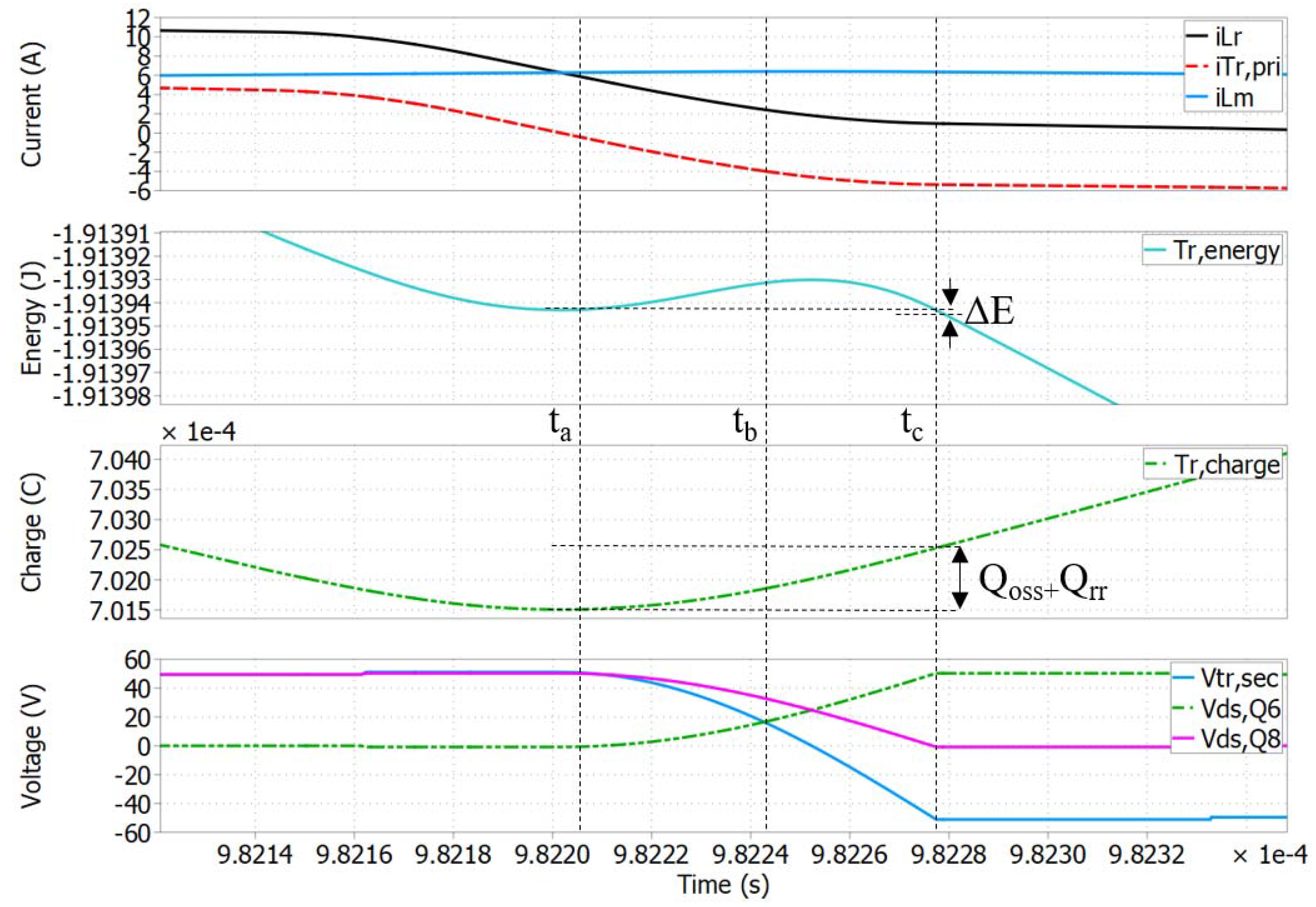
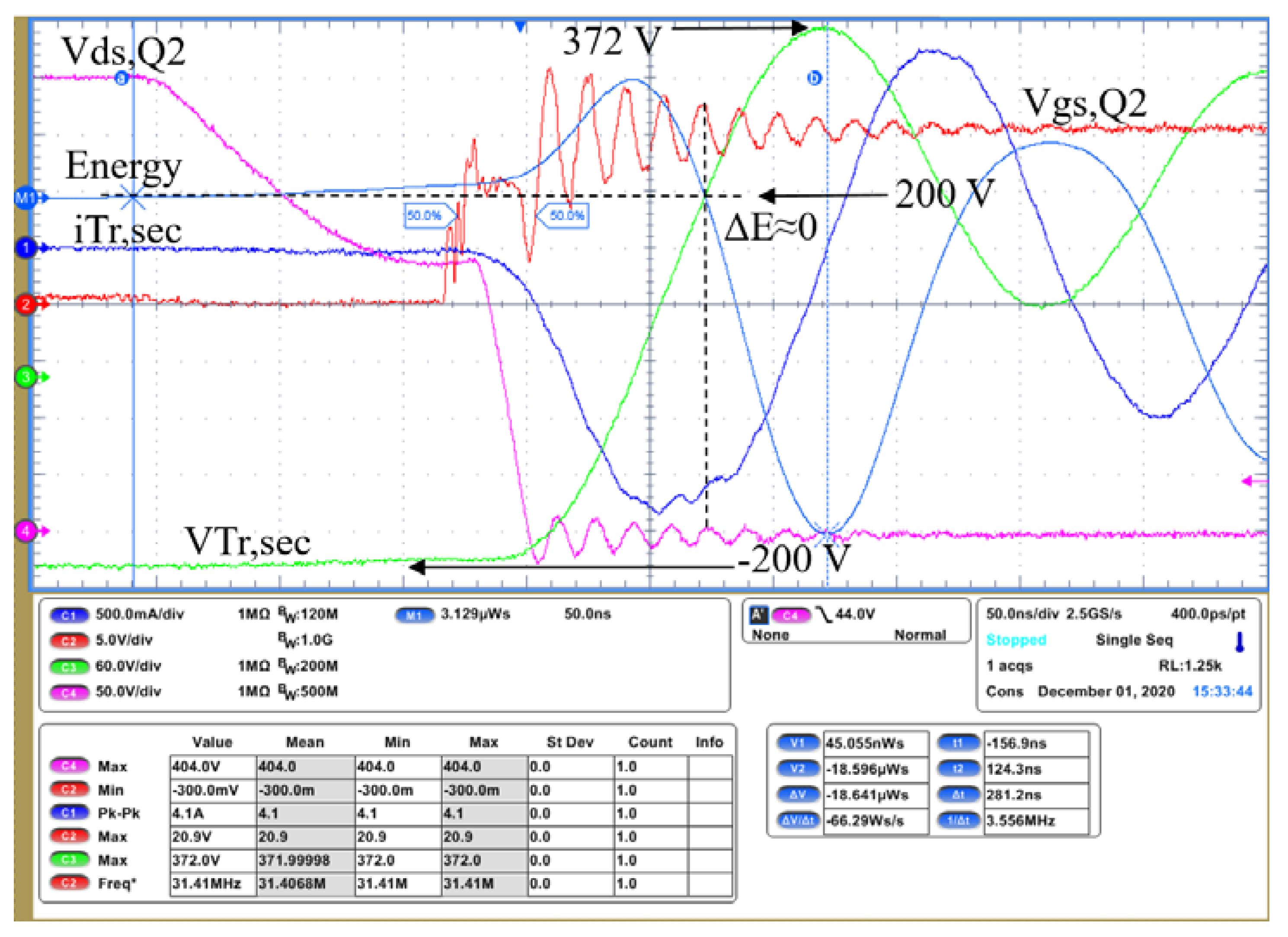
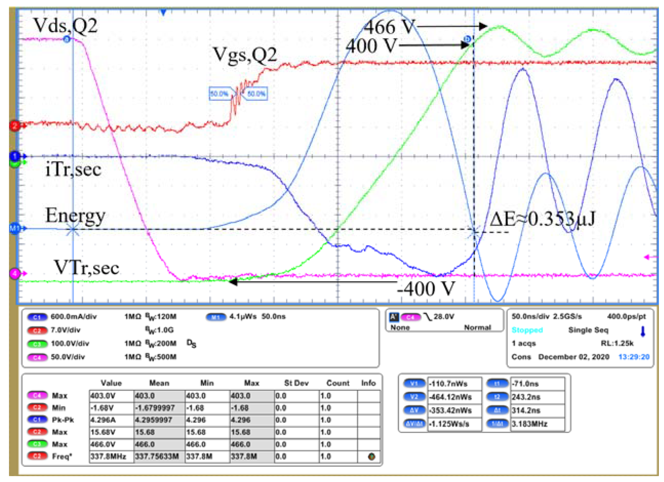
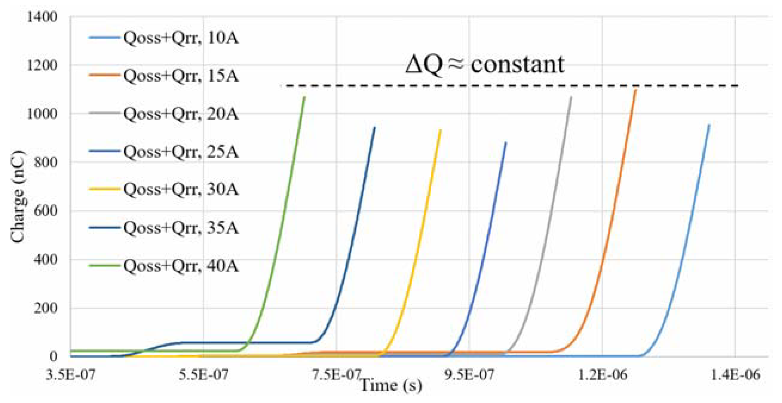
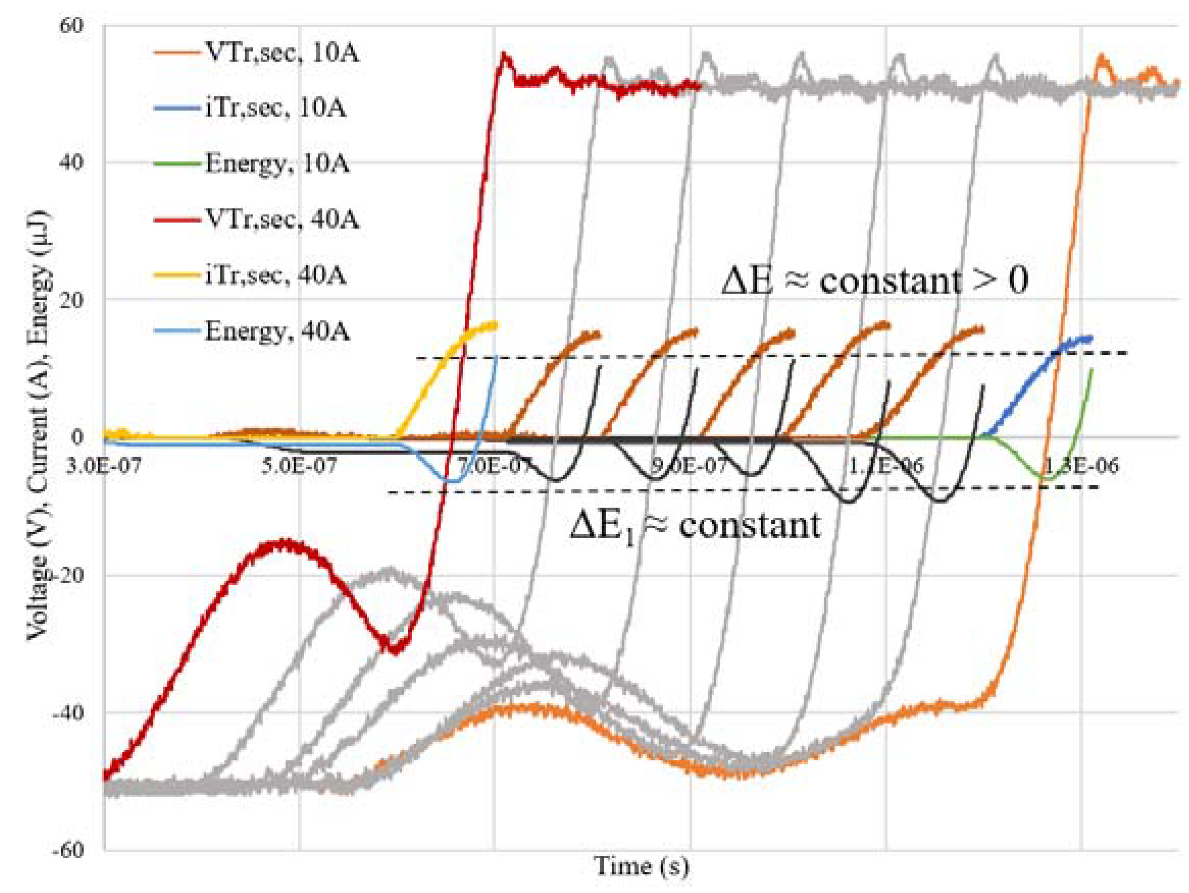
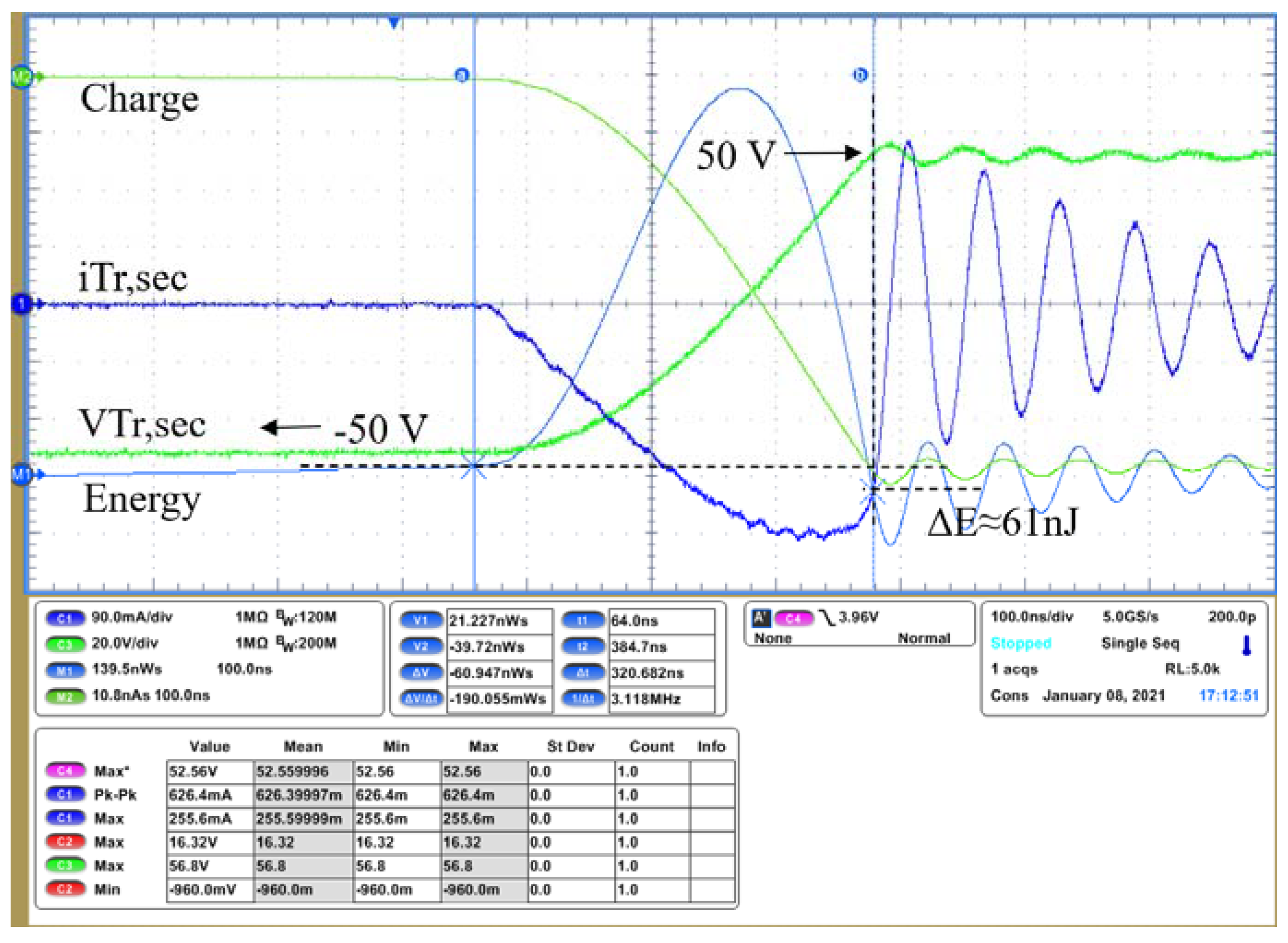
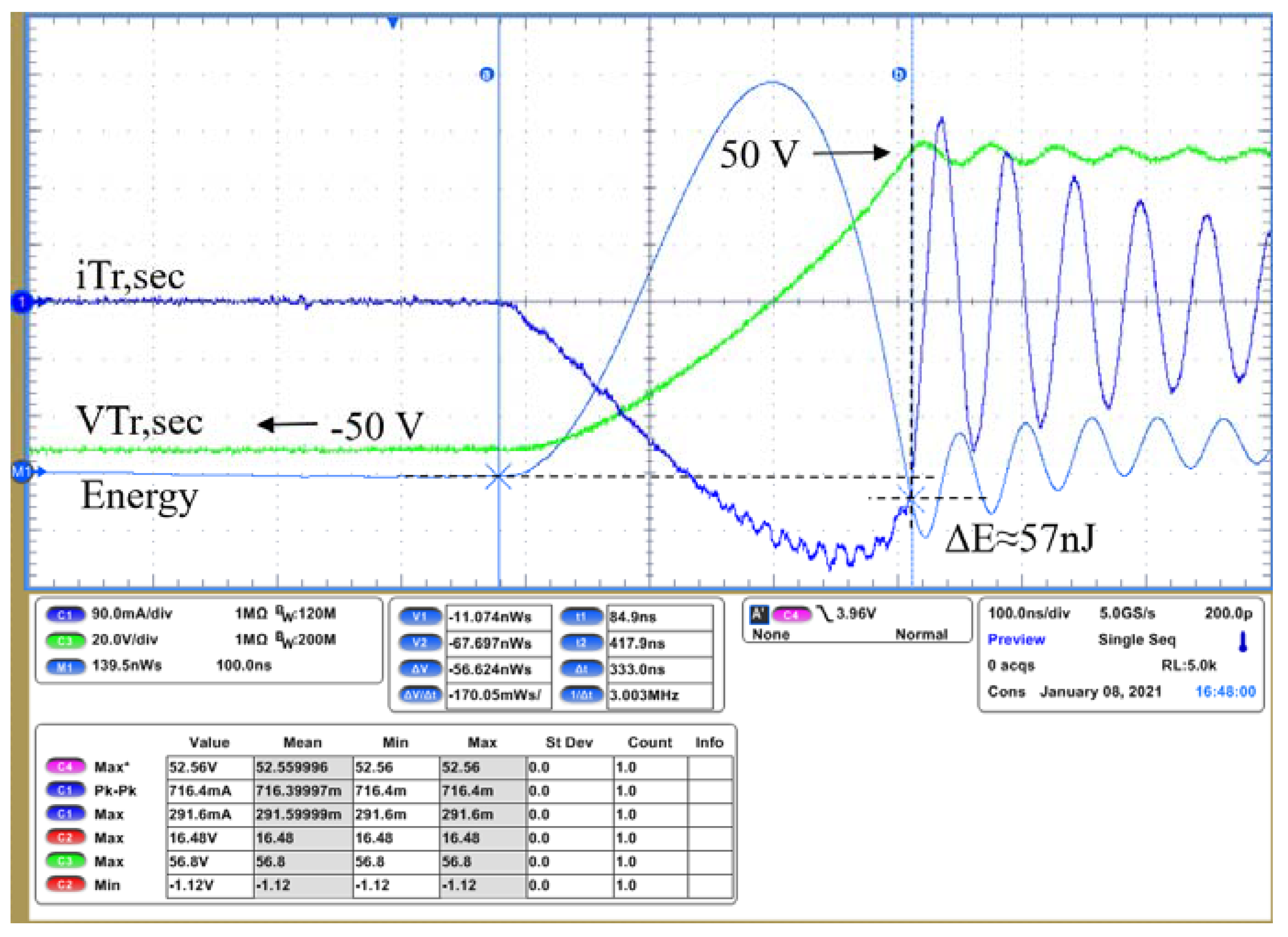
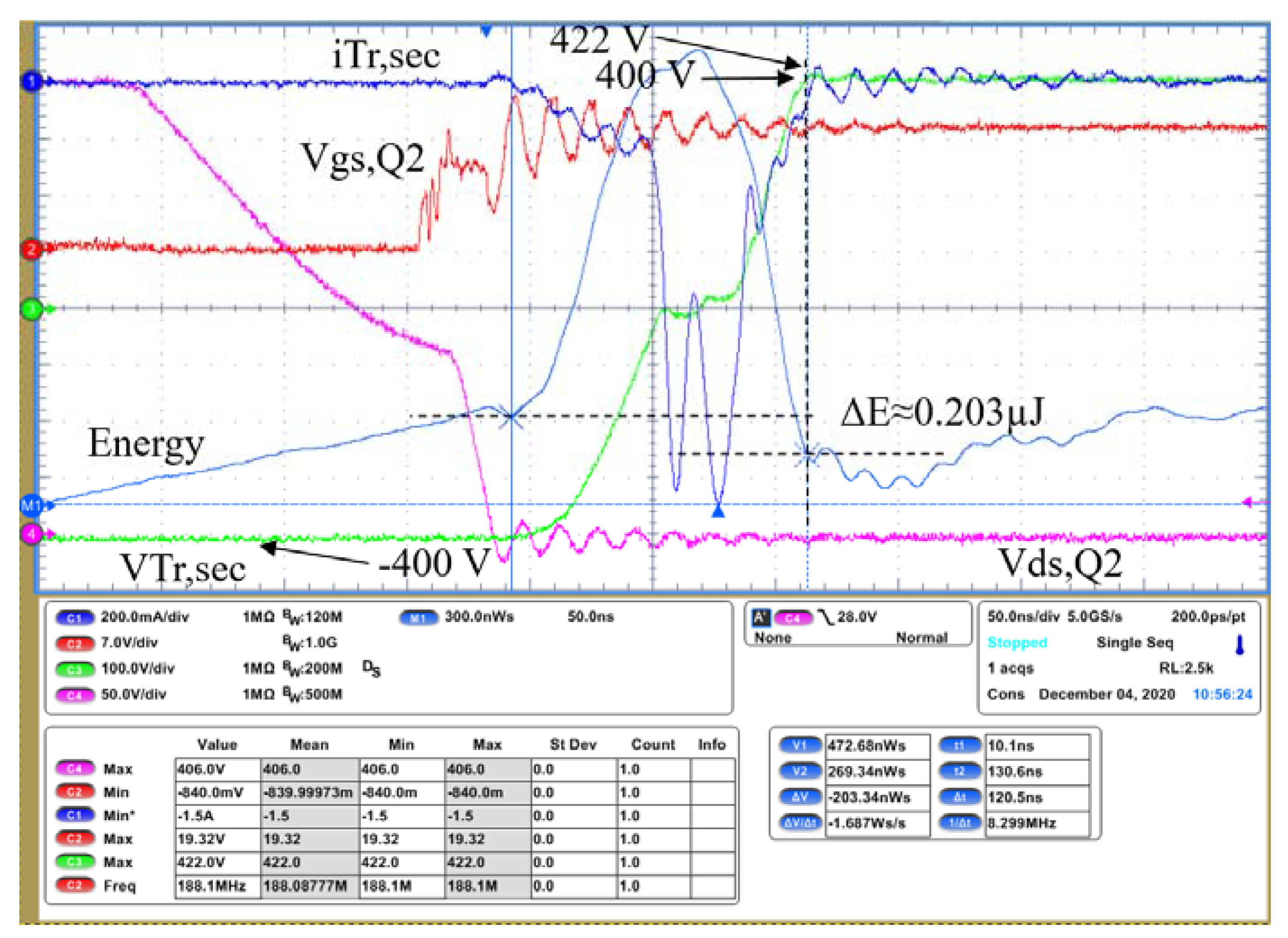
2.2. Measurement of Qoss, Qrr, and Switching Loss

During the commutation of the secondary side rectifiers, it is possible to measure, directly in the application, the stored charge (Qoss), the reverse recovery charge (Qrr), the stored energy (Eoss), and the total switching loss (Eloss) of the devices.
If the magnetizing inductance is realized with a discrete external inductor (Lm) and the main transformer is near ideal (its magnetizing inductance is much bigger than the external Lm) the total transferred charge, which includes Qoss and Qrr, can be calculated from the measurement of iLm and iLr by means of (2). The integral of the current shall be computed from the start of the commutation (ta) until the point where the antiparallel body diodes start to conduct (tc). The start of the commutation corresponds to the cross of iLr with iLm (Figure 7), whereas the end of the commutation can be estimated at the point where vTr,sec reaches the output voltage plus the diode forward drop (3).
Q oss + Q rr = Q = t a t c ( iL m iL r ) d t
{ iL m ( t a ) iL r ( t a ) = 0 vT r , sec ( t a ) = ( v out + v f ) vT r , sec ( t c ) = ( v out + v f )
The switching loss can be calculated by computing the balance of energy that flows through the transformer during the commutation. From the point of view of the transformer, from ta to tb energy is recovered during the charge and discharge of C5–C8. Inversely, from tb to tc energy is delivered (Figure 7). The point tb corresponds to the zero crossing of vTr,sec (4), where all the capacitors C5 to C8 have an equal voltage.
Notice that because no energy is being delivered to the output during the commutation of the rectifiers, if there were no losses, the total energy at the start and at the end of the transition shall be equal. However, if there is a difference between the measured energies at the start and at the end, it necessarily corresponds to losses, which can be attributed to the switching loss contribution of the rectifiers, and calculated with (5) and (6).
vT r , sec ( t b ) = 0
if   Q rr = 0 yields { E 1 = | t a t b ( iL m iL r ) · vT r , sec d t | E 2 = | t b t c ( iL m iL r ) · vT r , sec d t | E 2 E 1
E loss , 1 = E 2 E 1 = E
However, due to the effect of the reverse recovery charges (Qrr) the apparent energy balance could be smaller than the actual losses, even zero or negative (7). Therefore, the correct estimation of the total loss, including the Qrr contribution, requires a measurement that can exclude its effect, even more for semiconductor devices where the Qrr can be relatively large [30] (e.g., HV SJ Si MOSFETs [31] or LV Si shield-plate FETs [22]). For this purpose, a novel measurement setup is introduced in the next sections of this manuscript. Thereafter the Coss hysteresis loss (Eloss,1) can be substituted in (8) and (9) to subsequently obtain the Qrr component.
if   Q rr 0 yields { E 3 = | t a t b ( iL m iL r ) · vT r , sec d t | E 4 = | t b t c ( iL m iL r ) · vT r , sec d t | E 3 > E 1   &   E 4 E 2
E loss , 2 = ( E 3 E 1 ) + ( E 4 E 2 ) + ( E 2 E 1 ) = E 3 + E 4 2 E 1  
( E loss , 2 > E loss , 1 )   &   ( E loss , 2 > E )

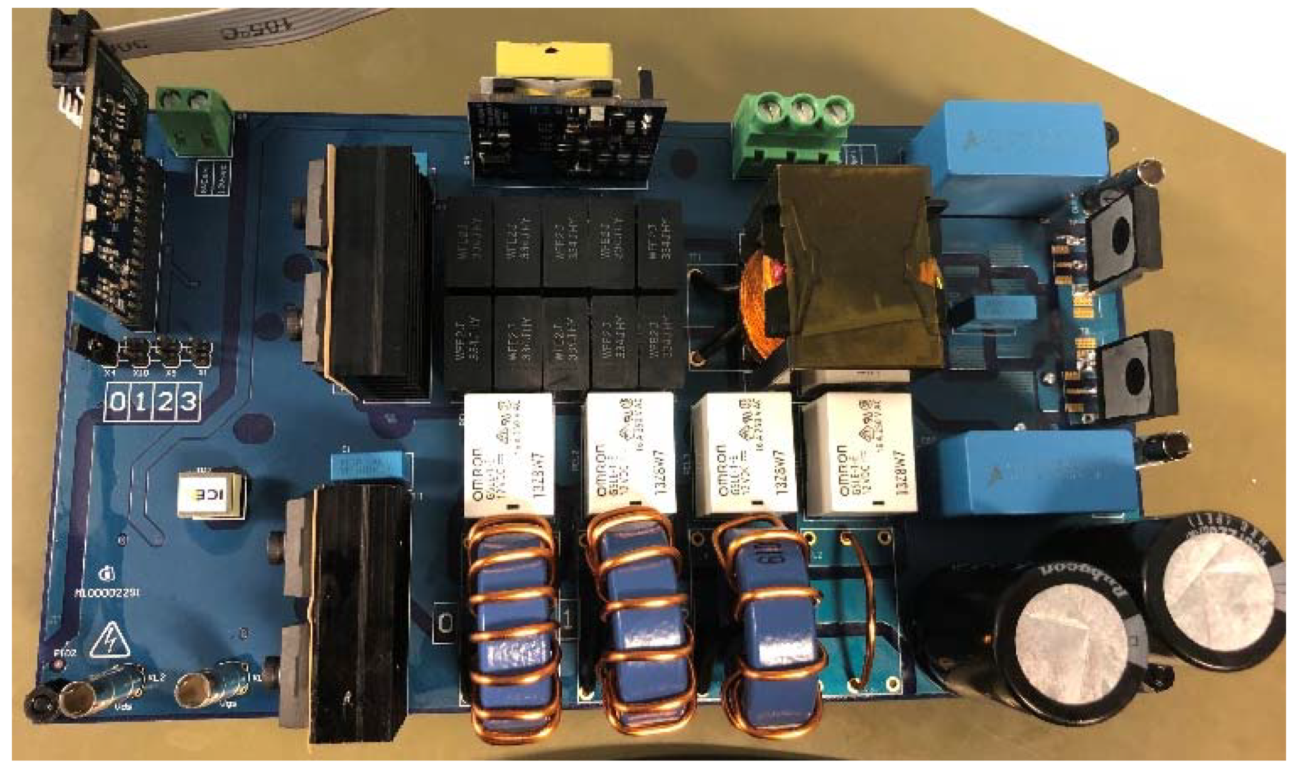
3. Testing Setup for the Isolation of Coss Loss

The principles of operation during the commutation of the rectifying devices in the LLC converter are utilized in two novel measurement circuits that isolate the loss due to the charge and discharge of the Coss and exclude other contributions, i.e., Qrr and conduction losses. These two circuits are introduced and analyzed in this section.

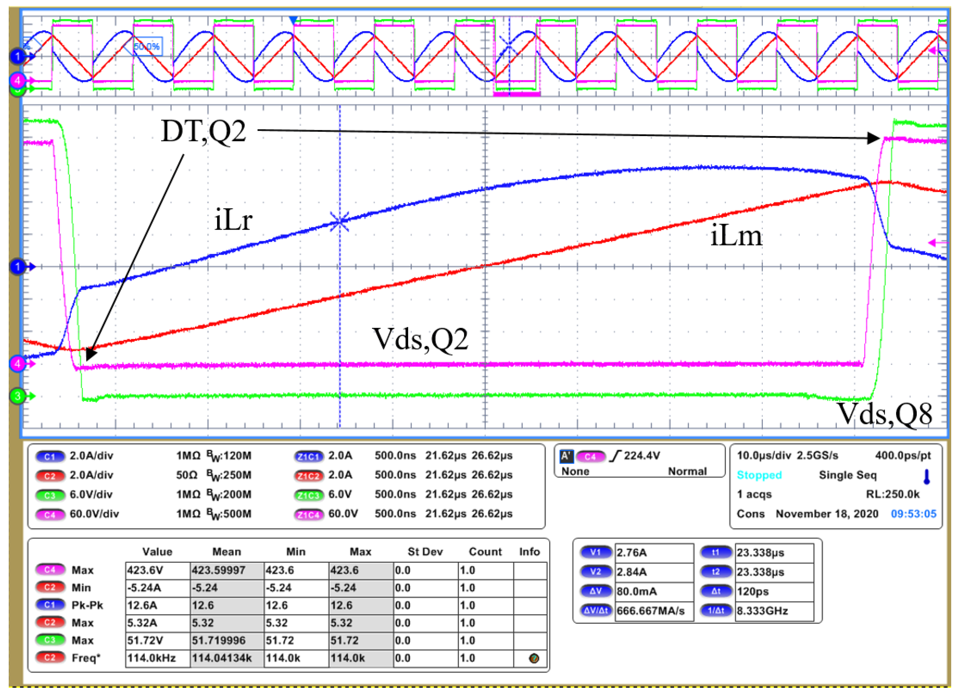
3.1. Back-To-Back Devices under Test

The first proposed circuit is represented in Figure 8, with its main differences to the original half-bridge LLC circuit in Figure 1 being that the output capacitance and the load of the converter have been removed, and the full-bridge rectification has been replaced by a back-to-back configuration of the Devices Under Test (DUTs).
Placing the DUTs in a back-to-back configuration ensures that their intrinsic body diodes or their channels do not conduct. As a result, we can exclude the Qrr in the computation of the switching loss which could mask the soft-switching losses, as was analyzed in the previous section. More importantly, the proposed circuit can be used for testing devices of very distinct voltages by only adapting the transformer turn ratio and/or the input voltage Vin. Whereas the same purpose could be achieved with the full-bridge configuration in Figure 1, it is convenient to reduce the number of required DUTs for the test.
Figure 9 shows the main driving signals and waveforms of the proposed circuit. Before the analysis some assumptions are made: (1) all diodes and switches are ideal; (2) all switches are MOSFETs with intrinsic antiparallel body diodes; (3) all capacitors and inductors are ideal; (4) C1 = C2, C5 = C6 = C7 = C8; (5) (C3 + C4) >> (C1 + C2); (6) Lm = ∞; (7) the switching frequency (Fsw) is greater than the series resonant frequency ( F r = 1 2 π L r ( C 3 + C 4 ) ); (8) the duty cycle is 50%. In the following paragraphs, we analyze its operation principles.
The primary high side device Q1 is on and its channel is conducting. The current through Lr (iLr) freewheels through one of the clamping diodes (D9). Since there is no current through the transformer (iTr,pri = zero), only the magnetizing current iLm flows towards Cr (C3 plus C4). We can consider Lm to be large enough that we can neglect its contribution.
In the secondary side of the converter, the voltage of the transformer VTr,sec is clamped thanks to the primary side diodes (D9 and D10), which holds true as far as the primary current continues to freewheel through one of them. The switching frequency of the circuit is adjusted to ensure that.
2.
Mode 2[t1] (Figure 10b)
Both primary side devices are off and their capacitances, C1 and C2, are being respectively charged and discharged by iLr, which continues to freewheel through D9.
3.
Mode 3[t2] (Figure 10c)
The voltage transition of the primary side devices ends and the intrinsic body diode D2 continues to conduct the freewheeling current. Notice that depending on the size of the capacitances, the transition of the primary side devices and the transition of the secondary side devices can overlap. Notice also that it might be possible that the primary side devices do not reach full ZVS turn-on. However, none of those phenomena have an impact on the proposed measurement technique of the secondary side switching losses.
4.
Mode 4[t3] (Figure 10d)
Q2 is on and its channel is conducting iTr,pri minus iLm. At the same time, the capacitance of Q8 is being discharged while the capacitance of Q6 is being charged. We can observe that Q6 and Q8 form a closed loop and the charge and energy is transferred back and forth from one to the other. Therefore, the proposed circuit works best when both devices are equal (C6 = C8) so all of their charge can be moved during the transition.
5.
Mode 5[t4] (Figure 10e)
Ideally, at this point no current should circulate through the transformer or the capacitances of the DUTs. However, due to non-idealities of the circuit, after the charge of C6 and the discharge of C8, the leakage of the transformer and other stray inductances cause a resonance and a subsequent overshoot in the secondary side devices (Figure 11).
It should be noted that the unwanted resonance and overshoot does not interfere with the proposed measurement technique. As was previously analyzed, Qoss and the energy have to be computed only between ta and tc. However, the overshoot may limit the measurement range when the peak voltage comes closer to the breakdown limit of the DUTs, e.g., in the capture in Figure 12, the overshoot reaches a peak of 372 V while measuring a charge-discharge of 200 V (i.e., 172 V of overshoot). Therefore, it is desirable to further improve the circuit and to reduce the effect of the stray inductances to a minimum.
The main sources of error are the inaccuracy and uncertainty of the voltage and current measurements and their relative shift (skew). It is essential to evaluate the influence of such parameters on the results. The sensitivity of the results for several of the DUTs to the variation of the gain in the voltage measurement (ΔV), the gain in the current measurement (ΔI), and the skew (Δskew) is shown in Figure 13, which indicates that the most sensitive parameter is the ΔV (unless for DUT3 in the graph). On the other hand, the current gain and the skew between the signals presented relatively minor sensitivity values.
It is worth highlighting that the LC resonance between the stray inductances and the capacitance of the DUTs at the end of the charge transition, e.g., in the measurement of a ceramic capacitor in Figure 12, can be used to adjust the skew between the current and voltage signals (i.e., the zero crossing of the current should match the peak amplitude of the voltage oscillation), therefore improving the accuracy of the proposed method. On the other hand, a possible offset in the measurement can be corrected in the post-processing of the data.

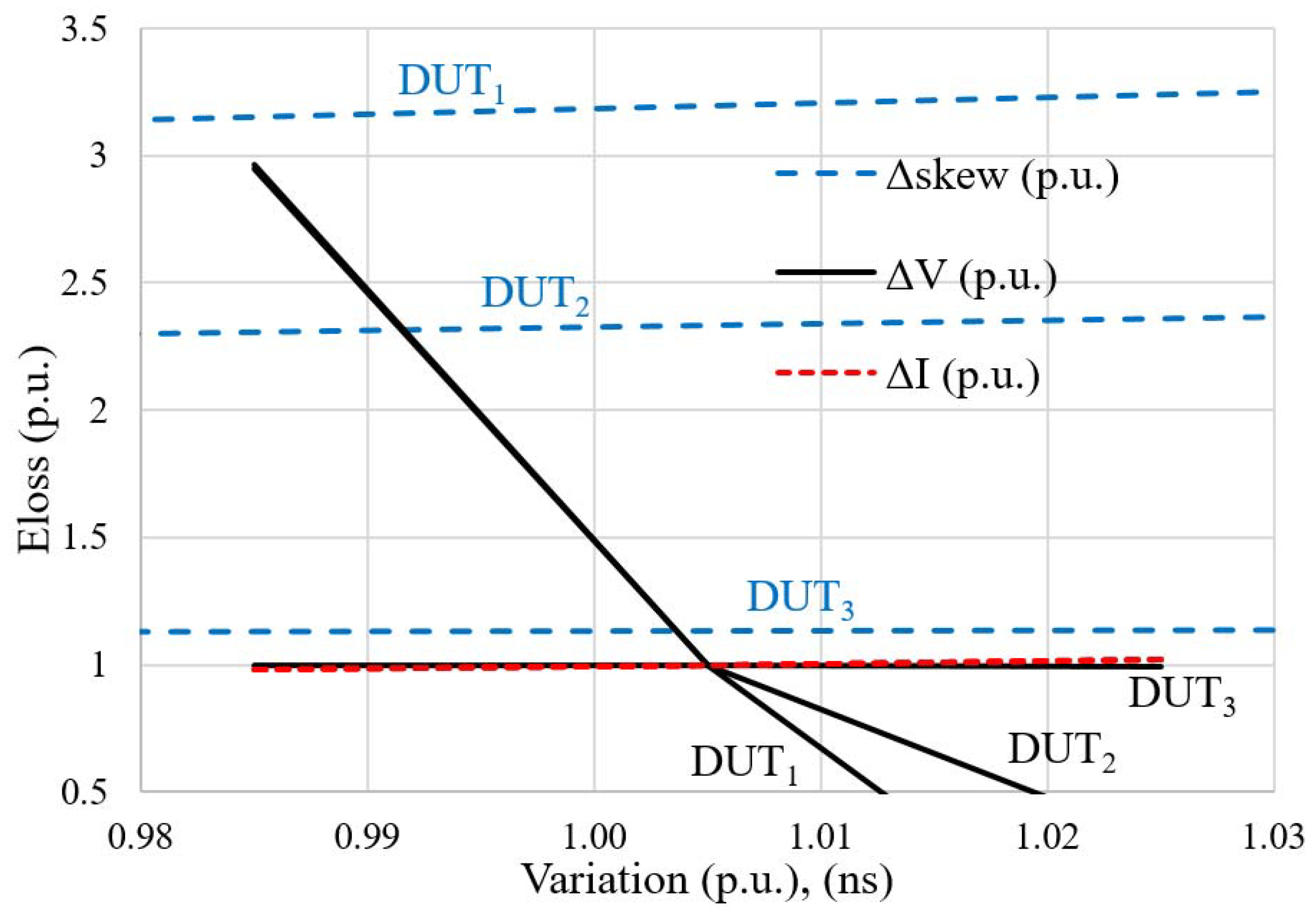
3.2. Improved Back-To-Back Configuration

The proposed measurement circuit in Figure 8 is further improved by moving the clamping diodes to the secondary side of the transformer (Figure 14). In this new configuration, the transformer ratio needs to be 1/2 (e.g., 8:16), for the clamping diodes to freewheel the current and clamp the DUTs voltage at the input supply rails. Thanks to this configuration, the current through the leakage of the transformer is also freewheeled through the clamping diodes. Moreover, other stray inductances can be reduced, placing the diodes as close as possible to the DUTs.
The working principles of the circuit in Figure 14 are equal to the working principles of the circuit in Figure 8. It is only required that the transformer current measurement is done between one of the DUTs and its clamping diodes (iCoss,sec), to exclude from the measurement in this manner the freewheeling current and the clamping diode capacitances.
In Figure 15, a 650 V SiC MOSFET is measured in the improved circuit configuration, charging and discharging 400 V while the peak of the overshoot only reaches 466 V (i.e., 66 V overshoot).

4. Experimental

The 3300 W LLC DCDC converter in [32], whose main specifications are listed Table 1, was modified to demonstrate the measurement techniques proposed in this work. The SRs in place during the experiments were a total of twenty-four NTMFS08N003C, six devices in parallel per position in the secondary side full-bridge. The main experimental results are summarized in this section.

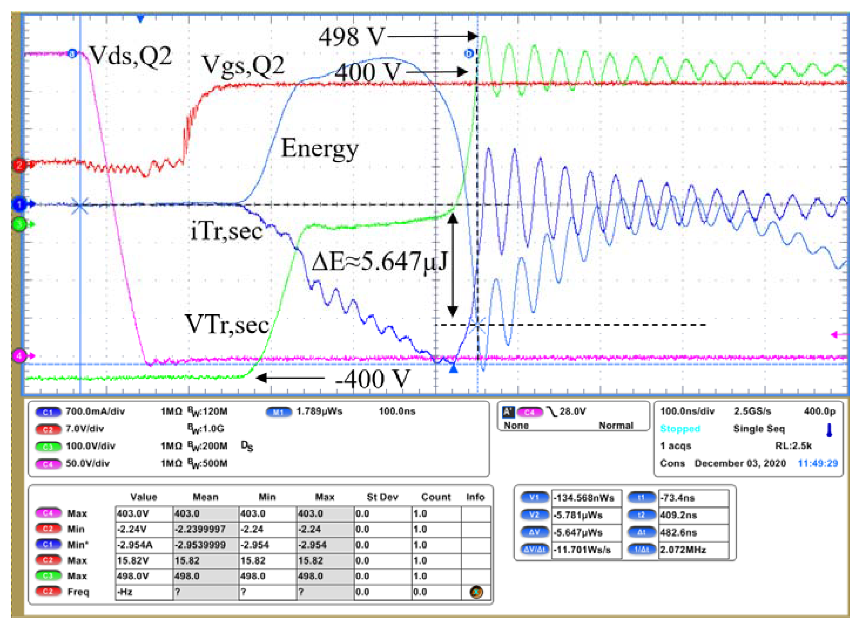
4.1. Low Voltage Rectifiers Coss Loss

The secondary side voltage vTr,sec and the primary side currents iLr and iLm were measured at different points of load, from 10 A to 40 A, and in two different operation modes: under resonance (400 V input and 50 V output) and above resonance (410 V input and 50 V output). The measurements of the voltage, the current, the integral of the charge and the integral of the energy are plotted in Figure 16 and Figure 17 for the operation under resonance, and Figure 18 and Figure 19 for the operation above resonance.
In the operation under resonance, sometimes referred to as DCM, a consistent ΔE around 8 µJ (Figure 17) and a consistent Qoss around 950 nC (Figure 16) can be observed. However, in the operation above resonance (where the rectifiers are commutated by the transformer), a noticeable increase in ΔE3 and an apparent decrease in ΔE (Figure 19) can be observed. Nevertheless, as was previously analyzed, this should not be interpreted as lossless transitions but as an effect of the additional Qrr. This is further corroborated by the noticeably load-dependent increase in the measured charge (Qoss plus Qrr) in Figure 18.
Two samples of the NTMFS08N003C were subsequently tested in the improved back-to-back proposed circuit to isolate the loss due to the charge-discharge of their output capacitance. The result is captured in Figure 20, where a hysteresis loss of approximately 61 nJ can be observed. To account for the total losses in the application, the 61 nJ is multiplied by the total number of devices (twenty-four), resulting in approximately 1.5 µJ. The discrepancy between this result and the previously estimated 8 µJ can be attributed to the different dv/dt, and therefore the relatively smaller currents passing through the lumped equivalent series resistance (Ross).
In addition, two early samples of a new LV MOSFET technology from Infineon (ISC033N08NM6) were also tested in the proposed back-to-back circuit. The result is captured in Figure 21, where a comparatively lower hysteresis loss of approximately 57 nJ can be observed.

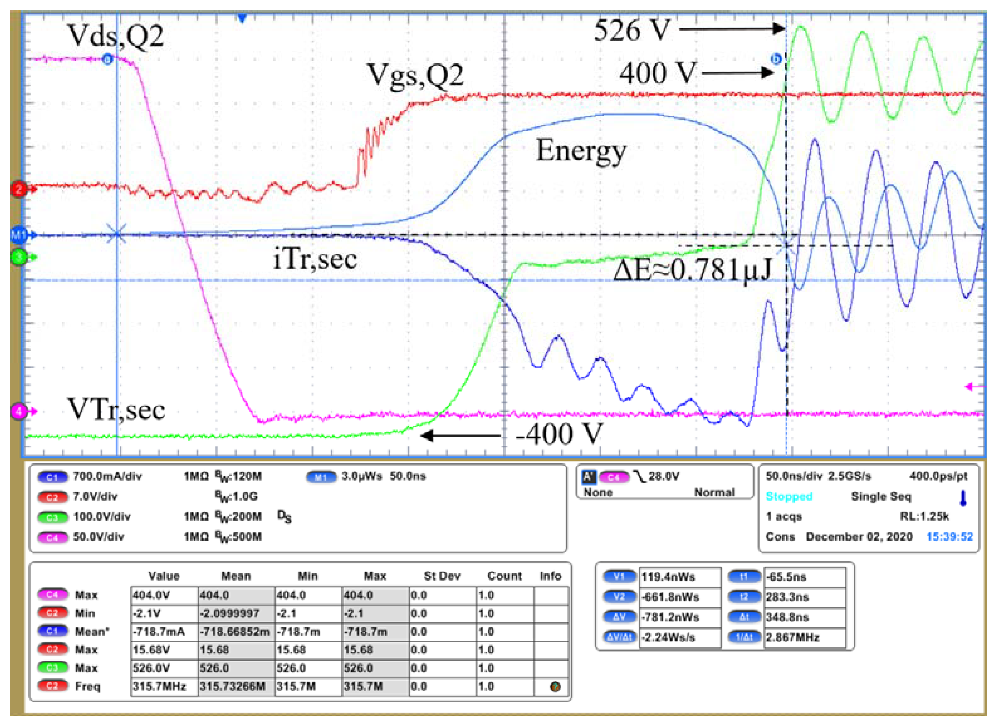
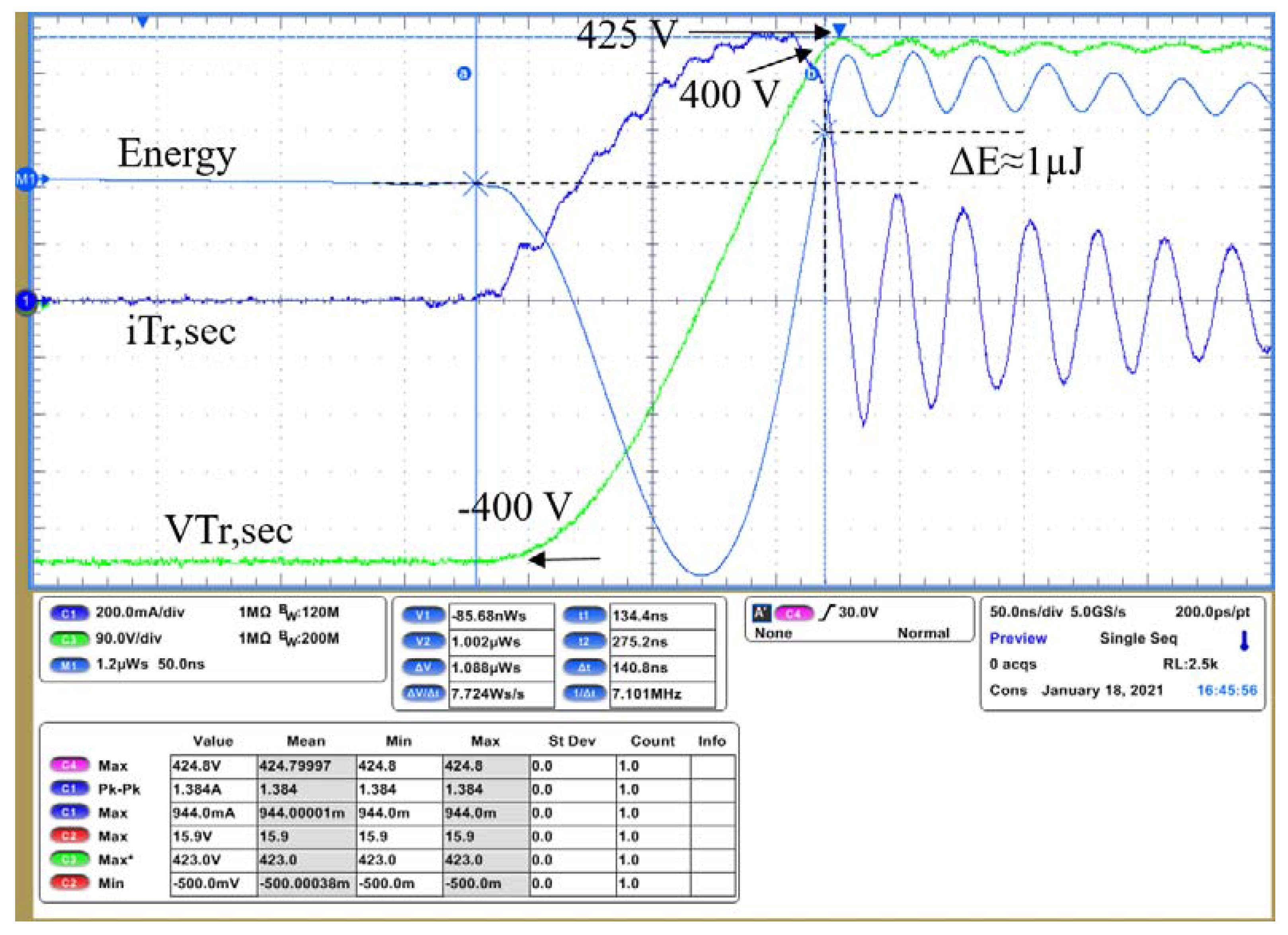
4.2. High Voltage MOSFETs Coss Loss

The LLC DCDC converter in [32] was further modified into the proposed improved measurement circuit in Figure 14 and applied to the measurement of the Coss hysteresis loss in HV MOSFETs. As a result, it is also possible to evaluate, with the same setup, the ZVS switching losses of the primary side devices in the LLC converter. Figure 22 is a top-view of the newly developed measurement platform, including the selectable series inductor to achieve variable dv/dt conditions.
Several examples of distinct HV MOSFETs technologies were measured while being charged-discharged at 400 V, which is a typical nominal input voltage in back-end DCDC converters as part of a complete PSU. In the experimental results, we compared a relatively old 650 V Silicon Super-Junction (SJ) technology (IPP65R065C7 in Figure 23), with a more modern 600 V Si SJ MOSFET of similar Rds,on (IPP60R070CFD7in Figure 24), and with a 650 V SiC MOSFET (IMW65R027M1H in Figure 15 and SCTW35N65G2VAG in Figure 25), and finally with a high-ohmic 700 V Si SJ MOSFET (IPAN70R900P7S in Figure 26). A summary of their results is presented in Table 2 together with the LV devices that were tested inside the LLC converter application in the previous section (NTMFS08N003C and ISC033N08NM6). This example highlights the convenience of the proposed method while underlining the superiority of the more recent technologies.

5. Conclusions

In this paper, it has been experimentally demonstrated that the contribution of the switching loss of the secondary side rectifiers in LLC resonant converters can have a noticeable impact on the overall losses in all the operation modes of the converter, therefore decreasing the final efficiency of the complete power supply unit [25].
The analysis of the commutation process of the secondary side rectifiers together with the measurement techniques proposed in this paper enable the accurate estimation of the switching loss contribution. The experimental results demonstrate that the switching loss of the rectifiers comprises two sources: the reverse recovery charges Qrr, especially (but not only) while operating the LLC above resonance; and the output capacitance Coss hysteresis loss, not reported elsewhere in low-voltage MOSFETs previously, and present in all the operation modes of the LLC.
The principles of operation of the proposed characterization techniques for the switching loss in the secondary side rectifiers in isolated converters were utilized in two novel circuits designed for the separation and the measurement of the Coss hysteresis loss of low-voltage and high-voltage semiconductor devices.
Finally, the Coss hysteresis loss of several high-voltage and low-voltage MOSFETs was experimentally verified in the proposed testing circuits.

Author Contributions

Conceptualization, M.E., M.-A.K. and F.P.; methodology, M.E. and F.P.; software, M.E.; validation, M.E., M.-A.K. and F.P.; formal analysis, M.E. and F.P.; investigation, M.E., M.-A.K., F.P., N.R. and D.P.M.; resources, M.-A.K.; data curation, F.P.; writing—original draft preparation, M.E.; writing—review and editing, M.E., N.R. and D.P.M.; visualization, M.E. and F.P.; supervision, M.-A.K., N.R. and D.P.M.; project administration, M.-A.K., N.R. and D.P.M. All authors have read and agreed to the published version of the manuscript.

Funding

This research received no external funding.

Institutional Review Board Statement

Not applicable.

Informed Consent Statement

Not applicable.

Data Availability Statement

Data sharing not applicable.

Acknowledgments

N.R. and D.P.M. thank Regional Government project P20_00265 and National Government Project PID2020-117344RBI00.

Conflicts of Interest

The authors declare no conflict of interest. The funders had no role in the design of the study; in the collection, analyses, or interpretation of data; in the writing of the manuscript, or in the decision to publish the results.

References

  1. Gautam, D.F.; Musavi, M.; Edington, W.E.; Dunford, W.G. An automotive on-board 3.3 kW battery charger for PHEV application. In Proceedings of the 2011 IEEE Vehicle Power and Propulsion Conference, Chicago, IL, USA, 5–8 September 2011; pp. 1–6. [Google Scholar]
  2. Tung, N.T.; Tuyen, N.D.; Huy, N.M.; Phong, N.H.; Cuong, N.C.; Phuong, L.M. Design and Implementation of 150 W AC/DC LED Driver with Unity Power Factor, Low THD, and Dimming Capability. Electronics 2020, 9, 52. [Google Scholar] [CrossRef] [Green Version]
  3. Yang, C.; Liang, T.; Chen, K.; Li, J.; Lee, J. Loss analysis of half-bridge LLC resonant converter. In Proceedings of the 2013 1st International Future Energy Electronics Conference (IFEEC), Tainan, Taiwan, 3–6 November 2013; pp. 155–160. [Google Scholar]
  4. Wang, Q.; Zhang, X.; Burgos, R.; Boroyevich, D.; White, A.; Kheraluwala, M. Design considerations for a high efficiency 3 kW LLC resonant DC/DC transformer. In Proceedings of the 2015 IEEE Energy Conversion Congress and Exposition (ECCE), Montreal, QC, Canada, 20–24 September 2015; pp. 5454–5461. [Google Scholar] [CrossRef]
  5. Jadli, U.; Mohd-Yasin, F.; Moghadam, H.A.; Pande, P.; Nicholls, J.R.; Dimitrijev, S. Measurement of Power Dissipation Due to Parasitic Capacitances of Power MOSFETs. IEEE Access 2020, 8, 187043–187051. [Google Scholar] [CrossRef]
  6. Schmidt, O.R.; Myhre, E. 380Vdc/48Vdc/ 3kw DC/DC converter with 98.2% efficiency. In Proceedings of the 2015 IEEE International Tele-com-munications Energy Conference (INTELEC), Osaka, Japan, 18–22 October 2015; pp. 1–6. [Google Scholar]
  7. Mu, M.; Lee, F.C. Design and Optimization of a 380V-12V High-Frequency, High-Current LLC Converter with GaN Devices and Planar Matrix Transformers. IEEE J. Emerg. Sel. Top. Power Electron. 2016, 4, 854–862. [Google Scholar] [CrossRef]
  8. Rogina, M.R.; Rodriguez, M.; Lamar, D.G.; Roig, J.; Vanmeerbeek, P.; Bauwens, F. Novel Selection Criteria of Primary Side Transistors for LLC Resonant Converters. In Proceedings of the 2018 IEEE 19th Workshop on Control and Modeling for Power Electronics (COMPEL), Padua, Italy, 25–28 June 2018; pp. 1–6. [Google Scholar] [CrossRef] [Green Version]
  9. Rothmund, D.; Bortis, D.; Kolar, J.W. Accurate Transient Calorimetric Measurement of Soft-Switching Losses of 10-kV SiC mosfets and Diodes. IEEE Trans. Power Electron. 2017, 33, 5240–5250. [Google Scholar] [CrossRef]
  10. Rogina, M.R.; Rodriguez, A.; Lamar, D.G.; Roig, J.; Gomez, G.; Vanmeerbeek, P. Analysis of Intrinsic Switching Losses in Super-junction MOSFETs Under Zero Voltage Switching. Energies 2020, 13, 1124. [Google Scholar] [CrossRef] [Green Version]
  11. Perera, N.; Kampitsis, G.; van Erp, R.; Ancay, J.; Jafari, A.; Nikoo, M.S.; Matioli, E. Analysis of Large-Signal Output Capacitance of Transistors Using Sawyer–Tower Circuit. IEEE J. Emerg. Sel. Top. Power Electron. 2020, 9, 3647–3656. [Google Scholar] [CrossRef]
  12. Jafari, A.; Nikoo, M.S.; Perera, N.; Yildirim, H.K.; Karakaya, F.; Soleimanzadeh, R.; Matioli, E. Comparison of Wide-Band-Gap Technologies for Soft-Switching Losses at High Frequencies. IEEE Trans. Power Electron. 2020, 35, 12595–12600. [Google Scholar] [CrossRef]
  13. Perera, N.; Nikoo, M.S.; Jafari, A.; Nela, L.; Matioli, E. Coss Loss Tangent of Field-Effect Transistors: Generalizing High-Frequency Soft-Switching Losses. IEEE Trans. Power Electron. 2020, 35, 12585–12589. [Google Scholar] [CrossRef]
  14. Zulauf, G.D.; Roig-Guitart, J.; Plummer, J.D.; Rivas-Davila, J.M. Coss Measurements for Superjunction MOSFETs: Limitations and Opportunities. IEEE Trans. Electron. Devices 2019, 66, 578–584. [Google Scholar] [CrossRef]
  15. Roig, J.; Gomez, G.; Bauwens, F.; Vlachakis, B.; Rogina, M.R.; Rodriguez, A.; Lamar, D.G. High-accuracy modelling of ZVS energy loss in advanced power transistors. In Proceedings of the 2018 IEEE Applied Power Electron-ics Conference and Exposition (APEC), San Antonio, TX, USA, 4–8 March 2018; pp. 263–269. [Google Scholar] [CrossRef] [Green Version]
  16. Tong, Z.; Roig-Guitart, J.; Neyer, T.; Plummer, J.D.; Rivas-Davila, J.M. Origins of Soft-switching Coss Losses in SiC Power MOSFETs and Diodes for Resonant Converter Applications. IEEE J. Emerg. Sel. Top. Power Electron. 2020, 9, 4082–4095. [Google Scholar] [CrossRef]
  17. Rutter, P. Considerations in the design of a low-voltage power MOSFET technology. IET Power Electron. 2019, 12, 3861–3869. [Google Scholar] [CrossRef]
  18. Rutter, P.; Peake, S.; Elford, A. Low voltage MOSFET optimized for low VDS transient voltages. In Proceedings of the 2013 25th International Symposium on Power Semiconductor Devices & IC’s (ISPSD), Kanazawa, Japan, 26–30 May 2013; pp. 83–86. [Google Scholar]
  19. Rutter, P.; Peake, S.T. Low voltage superjunction power MOSFET: An application optimized technology. In Proceedings of the 2011 Twenty-Sixth Annual IEEE Applied Power Electronics Conference and Exposition (APEC), Fort Worth, TX, USA, 6–11 March 2011; pp. 491–497. [Google Scholar]
  20. Williams, R.K.; Darwish, M.N.; Blanchard, R.A.; Siemieniec, R.; Rutter, P.; Kawaguchi, Y. The Trench Power MOSFET—Part I: History, Technology, and Prospects. IEEE Trans. Electron. Devices 2017, 64, 674–691. [Google Scholar] [CrossRef]
  21. Williams, R.K.; Darwish, M.N.; Blanchard, R.A.; Siemieniec, R.; Rutter, P.; Kawaguchi, Y. The Trench Power MOSFET—Part II: Application Specific VDMOS, LDMOS, Packaging, and Reliability. IEEE Trans. Electron. Devices 2017, 64, 692–712. [Google Scholar] [CrossRef]
  22. Roig, J.; Mouhoubi, S.; De Pestel, F.; Martens, N.; Bauwens, F.; Massie, H.; Golonka, L.; Loechelt, G. Body-diode related losses in Shield-Plate FETs for SiP 12V-input DC/DC buck converters operating at high-frequency (4MHz). In Proceedings of the 2012 24th International Symposium on Power Semiconductor Devices and ICs, Bruges, Belgium, 3–7 June 2012; pp. 291–294. [Google Scholar] [CrossRef]
  23. Roig, J.; Tong, C.-F.; Bauwens, F.; Gillon, R.; Massie, H.; Hoggatt, C. Internal self-damping optimization in trench power FETs for high-frequency conversion. In Proceedings of the 2014 IEEE Applied Power Electronics Conference and Exposition-APEC, Fort Worth, TX, USA, 16–20 March 2014; pp. 137–142. [Google Scholar] [CrossRef]
  24. Chen, J. Design optimal built-in snubber in trench field plate power MOSFET for superior EMI and efficiency performance. In Proceedings of the 2015 International Conference on Simulation of Semiconductor Processes and Devices (SISPAD), Washington, DC, USA, 9–11 September 2015; pp. 459–462. [Google Scholar] [CrossRef]
  25. Escudero, M.; Kutschak, M.A.; Meneses, D.; Rodriguez, N.; Morales, D.P. High Efficiency, Narrow Output Range and Extended Hold-Up Time Power Supply with Planar and Integrated Magnetics for Server Applications, PCIM Europe digital days 2021. In Proceedings of the International Exhibition and Conference for Power Electronics, Intelligent Motion, Renewable Energy and Energy Management, Nuremberg, Germany, 4–6 May 2021; pp. 1–8. [Google Scholar]
  26. Kim, J.-W.; Park, M.-H.; Lee, B.-H.; Lai, J.-S. Analysis and Design of LLC Converter Considering Output Voltage Regulation Under No-Load Condition. IEEE Trans. Power Electron. 2019, 35, 522–534. [Google Scholar] [CrossRef]
  27. Siemenic, R.; Braz, C. Impact of Synchronous Rectification MOSFET Capacitance on the Overall Efficiency of LLC converters, ISPS 2018, Prague. Available online: https://www.researchgate.net/publication/329738328_Impact_of_synchronous_rectification_MOSFET_capacitance_on_the_overall_efficiency_of_LLC_converters (accessed on 1 February 2021).
  28. Kim, J.; Kim, C.; Kim, J.; Moon, G. Analysis for LLC resonant converter considering parasitic components at very light load condition. In Proceedings of the 8th International Conference on Power Electronics-ECCE Asia, Jeju, Korea, 30 May–3 June 2011; pp. 1863–1868. [Google Scholar]
  29. Wen, H.; Gong, J.; Zhao, X.; Yeh, C.; Lai, J. Analysis of Diode Reverse Recovery Effect on ZVS Condition for GaN-Based LLC Resonant Converter. IEEE Trans. Power Electron. 2019, 34, 11952–11963. [Google Scholar] [CrossRef]
  30. Reid, M.D.; Round, S.; Duke, R. Modelling the temperature dependent reverse recovery behaviour of power diodes. In Proceedings of the International Power Electronics Conference, Tokyo, Japan, 3–7 April 2000; pp. 779–783. [Google Scholar]
  31. Jahdi, S.; Alatise, O.; Bonyadi, R.; Alexakis, P.; Fisher, C.A.; Gonzalez, J.A.O.; Ran, L.; Mawby, P. An Analysis of the Switching Performance and Robustness of Power MOSFETs Body Diodes: A Technology Evaluation. IEEE Trans. Power Electron. 2014, 30, 2383–2394. [Google Scholar] [CrossRef] [Green Version]
  32. Kutschak, M.; Escudero, M. 3300 W 52 V LLC with 600 V CoolMOS™ CFD7 and XMC™. Available online: https://www.infineon.com/cms/en/product/evaluation-boards/eval_3k3w_llc_hb_cfd7/ (accessed on 1 February 2020).
Figure 1. Half-bridge LLC DCDC converter with full-bridge rectification.
Energies 14 05915 g001
Figure 2. Measured efficiency of the 3 kW half-bridge LLC at the nominal input and output voltages and with two different resonant tank configurations: Lr = 6.1 µH (93 kHz) and Lr = 4.36 µH (110 kHz).
Energies 14 05915 g002
Figure 3. Main waveforms in the half-bridge LLC during the commutation of the secondary side rectifiers.
Energies 14 05915 g003
Figure 4. Main operation modes of the half-bridge LLC converter during the commutation of the rectifiers: (a) [t0]; (b) [t1]; (c) [t2]; (d) [t3]; (e) [t4]; (f) [t5].
Energies 14 05915 g004
Figure 5. Main waveforms of the 3 kW half-bridge LLC at 10 A of load. SRs dead time (DT).
Energies 14 05915 g005
Figure 6. Main waveforms of the 3 kW half-bridge LLC at 20 A of load.
Energies 14 05915 g006
Figure 7. Main waveforms in the half-bridge LLC during the commutation of the rectifiers. Measured charge and energy during the commutation.
Energies 14 05915 g007
Figure 8. Proposed circuit configuration for the measurement of the Coss hysteresis loss.
Energies 14 05915 g008
Figure 9. Main waveforms of the proposed circuit for the measurement of the Coss hysteresis loss.
Energies 14 05915 g009
Figure 10. Main operation modes for the proposed circuit for the measurement of the Coss hysteresis: (a) [t0]; (b) [t1]; (c) [t2]; (d) [t3]; (e) [t4].
Energies 14 05915 g010
Figure 11. Main waveforms in the proposed circuit for the measurement of the Coss hysteresis loss including the effect of Llkg and stray inductances.
Energies 14 05915 g011
Figure 12. Measurement of the hysteresis loss of a high-quality 330 pF ceramic capacitor. Near zero energy is lost during the charge and discharge.
Energies 14 05915 g012
Figure 13. Sensitivity analysis of the Coss hysteresis loss (Eloss) with respect to the varying parameters: skew (Δskew), voltage measurement gain (ΔV), and current measurement gain (ΔI).
Energies 14 05915 g013
Figure 14. Alternative, improved circuit for the measurement of the hysteresis loss in Coss.
Energies 14 05915 g014
Figure 15. Measurement of the hysteresis loss of IMW65R027M1H. Approximately 0.35 µJ are lost during the discharge and charge from 400 V to zero V and from zero V to 400 V.
Energies 14 05915 g015
Figure 16. Measured transferred charge in the secondary side of the 3 kW half-bridge LLC converter during the commutation of the rectifiers. DCM operation.
Energies 14 05915 g016
Figure 17. Measured transformer voltage and current in the secondary side of the 3 kW half-bridge LLC converter and the calculated accumulated energy during the commutation of the rectifiers. A positive offset in the energy indicates a loss. DCM operation.
Energies 14 05915 g017
Figure 18. Measured transferred charge in the secondary side of the 3 kW half-bridge LLC converter during the commutation of the rectifiers. CCM operation.
Energies 14 05915 g018
Figure 19. Measured transformer voltage and current in the secondary side of the 3 kW half-bridge LLC converter and the calculated accumulated energy during the commutation of the rectifiers. A positive offset indicates a loss. CCM operation.
Energies 14 05915 g019
Figure 20. Measured hysteretic loss of NTMFS08N003C. Approximately 61 nJ.
Energies 14 05915 g020
Figure 21. Measured hysteretic loss of ISC033N08NM6. Approximately 57 nJ.
Energies 14 05915 g021
Figure 22. Coss hysteresis loss measurement platform. The DUTs can be soldered to the multi-package pads on the top-right side of the image (e.g., the two standing TO-247 without a heatsink in this image).
Energies 14 05915 g022
Figure 23. Measured hysteretic loss of IPP65R065C7. Approximately 5.65 µJ.
Energies 14 05915 g023
Figure 24. Measured hysteretic loss of IPP60R070CFD7. Approximately 0.78 µJ.
Energies 14 05915 g024
Figure 25. Measured hysteretic loss of SCTW35N65G2VAG. Approximately 1 µJ.
Energies 14 05915 g025
Figure 26. Measured hysteretic loss of IPAN70R900P7S. Approximately 0.203 µJ.
Energies 14 05915 g026
Table 1. Key specifications of the prototype.
ParameterValue
Nominal input voltage410 V
Input voltage range320–430 V
Nominal output voltage50 V
Maximum output power3000 W
Target peak efficiency98.5%
Switching frequency70–150 kHz
Magnetizing inductance (Lm)65 µH
Resonant capacitor (Cr)480 nF
Turn ratio of the transformer16:4
Table 2. Summary of device characteristics.
VDS,MAX (V) @ 25 °CRDS,ON @ 25 °CELOSS (µJ)
IPP65R065C765065 mΩ5.65 @ 400 V
SCTW35N65G2VAG65067 mΩ1 @ 400 V
IPP60R070CFD760070 mΩ0.78 @ 400 V
IMW65R027M1H65034 mΩ0.35 @ 400 V
IPAN70R900P7S700900 mΩ0.203 @ 400 V
NTMFS08N003C803.1 mΩ0.061 @50 V
ISC033N08NM6803.3 mΩ0.057 @50 V
Publisher’s Note: MDPI stays neutral with regard to jurisdictional claims in published maps and institutional affiliations.

