Article

Interfacial Thermal Conductance across Graphene/MoS2 van der Waals Heterostructures

1
Merchant Marine College, Shanghai Maritime University, Pudong New Area, Shanghai 201306, China
2
School of Science, Shanghai Polytechnic University, Pudong New Area, Shanghai 201209, China
3
School of Environmental and Material Engineering, College of Engineering, Shanghai Polytechnic University, Pudong New Area, Shanghai 201209, China
4
Department of Mechanical and Aerospace Engineering, Rutgers, The State University of New Jersey, Piscataway, 08854 NJ, USA
*
Authors to whom correspondence should be addressed.
Energies 2020, 13(21), 5851; https://doi.org/10.3390/en13215851
Submission received: 11 October 2020 / Revised: 5 November 2020 / Accepted: 6 November 2020 / Published: 9 November 2020
(This article belongs to the Special Issue Heat Transfer and Thermal Management: From Nano to Micro-Scale)

Abstract

:
The thermal conductivity and interface thermal conductance of graphene stacked MoS2 (graphene/MoS2) van der Waals heterostructure were studied by the first principles and molecular dynamics (MD) simulations. Firstly, two different heterostructures were established and optimized by VASP. Subsequently, we obtained the thermal conductivity (K) and interfacial thermal conductance (G) via MD simulations. The predicted Κ of monolayer graphene and monolayer MoS2 reached 1458.7 W/m K and 55.27 W/m K, respectively. The thermal conductance across the graphene/MoS2 interface was calculated to be 8.95 MW/m2 K at 300 K. The G increases with temperature and the interface coupling strength. Finally, the phonon spectra and phonon density of state were obtained to analyze the changing mechanism of thermal conductivity and thermal conductance.

Graphical Abstract

1. Introduction

Due to high carrier mobility [1], high thermal conductivity [2], and ultra-high Young’s modulus [3], graphene has been widely used in the fields of energy storage [4], optoelectronics [5], and sensors [6]. The MoS2 as one kind of transition metal sulfides (TMDs), which overcomes graphene’s zero-bandgap, has been used as a catalyst to generate hydrogen [7] and in photothermal conversion area [8]. The heterostructures is the two-dimensional (2D) layered materials stacked by van der Waals (vdW) forces. It can be integrated into complex devices applied in photodetectors [9], photocatalytic, molecular sieves, and electrodes [10]. Ren et al. [11] reported that the TMDs/BN (boron nitride) vertical heterostructures have a direct bandgap and excellent optical properties. It can be applied to photocatalytic, photovoltaic, and optical areas. Chen et al. [12] fabricated MoTe2/MoS2 hetero-structures. It has a fast response and a broad wavelength range and can be applied to photodetection and on-chip logic circuits. Li et al. [13] prepared graphene/silicene heterostructures and proved weak van der Waals interactions between layers. The vertical graphene/silicene/Ru(Ruthenium) heterostructures show well Schottky rectification behavior.
The electrical and optical properties of graphene/MoS2 heterostructures have been studied. Biroju et al. [14] prepared monolayer graphene with a single or a few layered MoS2 van der Waals vertical heterostructures and studied the catalytic activity mechanism by the density functional theory (DFT). The heterostructures that graphene is over the MoS2 showed higher photo-response and hydrogen evolution reaction activity. The work of Safeer et al. [15] showed the spin effect in the graphene/MoS2 heterostructure and proved a superimposed spin-to-charge current conversion in the device based on it. Sun et al. [16] reported that the saturable absorption of graphene/MoS2 hetero-structure is adjustable by changing the thickness of MoS2. Furthermore, the structure can be applied in solid-state lasers, which can generate ultrafast pulses.
The development of applications with graphene/MoS2 vdW heterostructures requires the thermal management of these structures. Gong et al. [17] developed a model of monolayer graphene/Li/monolayer MoS2. The heterostructures’ electrical conductivity is higher than that of the MoS2, and the thermal conductivity of graphene/monolayer MoS2 with three graphene layers can maintain 85.5 W/m K at 100~500 K by molecular dynamics. Zhang et al. [18] simulated MoS2/graphene hybrid nanosheet (MGHN) structures and calculated thermal conductivity by molecular dynamics. In the simulation, heat baths are applied to both the MoS2 and graphene layers. The results show that the graphene layer in the MGHN structure can transfer most heat. It has a very high thermal conductivity and can be tuned by the interlayer coupling strength, temperature, and contact area. Oh et al. [19] stacked the fingerprint-like randomly aligned graphene nanoribbons on the monolayer MoS2 by block copolymer (BCP) lithography. The electrical conductivity and power factor of the hetero-structure are 902 S m−1 and 222.1 µW m−1 K−2. The hetero-junction network has superior thermoelectric properties and may be applied in next-generation electronic and energy devices. Therefore, understanding of van der Waals heterostructures’ thermal transport is essential for future use in optoelectronic and thermo-electronic applications. Previous researches investigated the thermal properties of graphene/MoS2 with different lengths, layers, and strain by experiment and simulation. However, few focused on different initial cell structures and defect effects on heterostructure thermal conductivity.
In this work, two graphene/MoS2 van der Waals heterostructures were established and investigated by the density functional theory (DFT). The bilayer nanoribbons were established, then the thermal conductivity and thermal conductance were obtained by molecular dynamics. We analyzed the thermal conductivity with different lengths, temperature, defect type, and defect concentration. The interfacial thermal conductance across the interface with different temperature and interface coupling strengths were calculated subsequently. We also obtained the phonon spectra to analyze defects and the coupling strength effects on the bilayer system thermal transports.

2. Simulation Methods

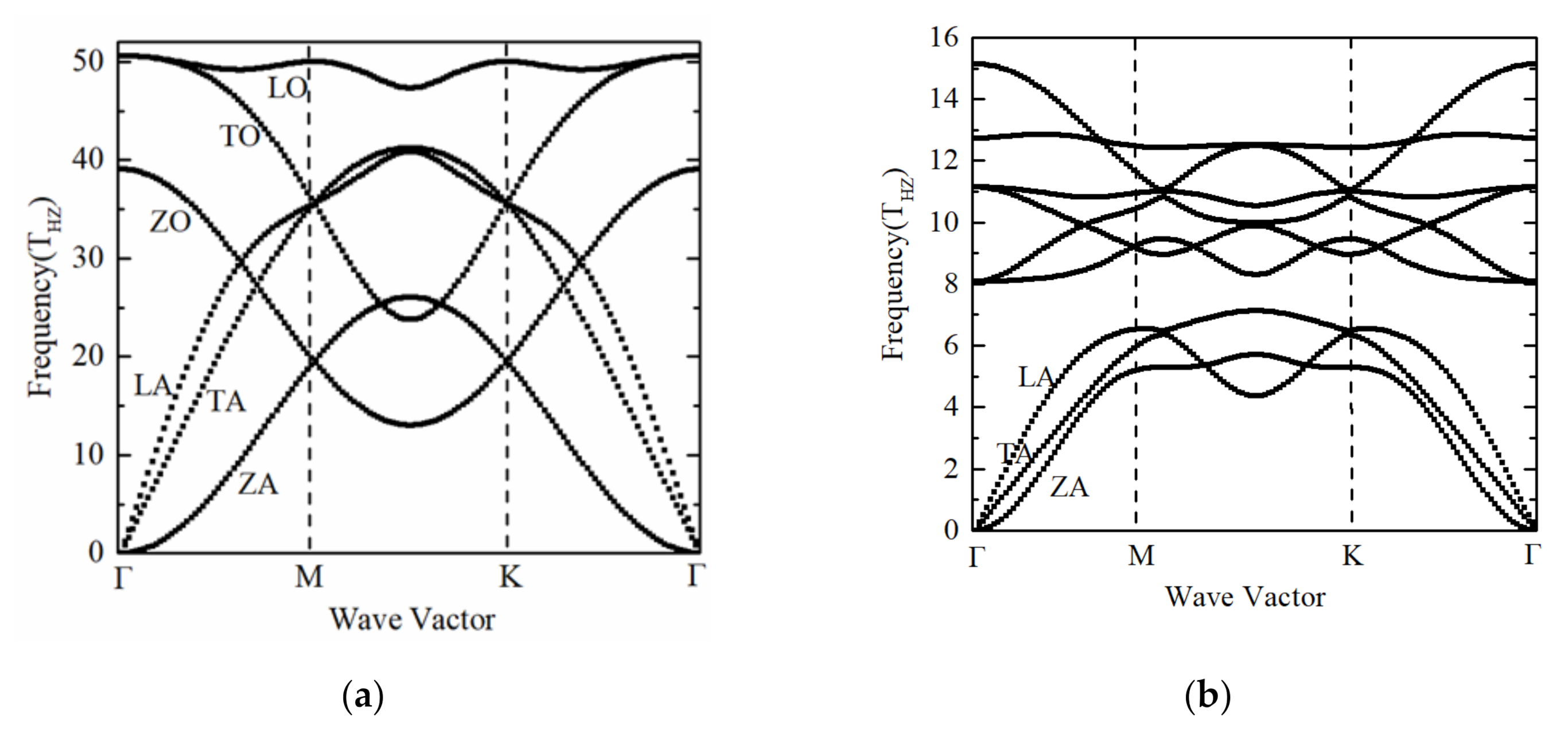
2.1. DFT Calculations

The establishment of geometries and energy calculation are based on DFT performed by software VASP (Vienna ab-initio Simulation Package) [20]. Here we used the projector-augmented wave (PAW) method to describe the electron-ion interactions. GGA-PBE [21] exchange-correlation function was selected for describing the interactions, and DFT-D2 [22] method was applied to describe van der Waals forces between layers. We stacked a monolayer of graphene whose supercell is 5 × 5 × 1 and a monolayer of MoS2 whose supercell is 4 × 4 × 1. The lattice constants of monolayer graphene and MoS2 are shown in Table 1. As in the previous First-principles study, the parameters are the same and agree with the experimental data.
Two structures are selected; for the first structure (Structure 1) shown in Figure 1a, the lattice constant of aH was taken as 12.26 Å [23], which is the optimized graphene lattice constant (aG). The lattice constant of MoS2 (aM) and the interlayer spacing were taken as 3.12 Å and 3.37 Å, respectively. A vacuum layer of 25 Å is added to reduce the interaction between the periodic structures in the Z-direction. And, for the second structure (Structure 2), aG = 2.47 Å, and aM = 3.16 Å [24]. The lattice mismatch ratio of it was about 2.3%. The lattice constant of aH is 12.46 Å after optimized, and the distance between layers shown in Figure 1c is 3.32 Å. The cut-off energy of the plane wave was taken as 550 eV for structure 1, and then another is 500 eV. The electronic iterations convergence was determined as 1.00 × 10⁻⁵ eV using the Normal (blocked Davidson) algorithm, and the structure relaxations finished when the convergence precision of each interatomic force reached 0.02 eV/Å. The 3 × 3 × 1 and 6 × 6 × 1 Monkhorst–Pack characteristic K points were adopted for geometries optimization. The building energy (Eb) per carbon atom between graphene and MoS2 is calculated as:
E b = E G / M E G E M / N C
where, EG/M, EG, EM are energies of the heterostructure, isolated monolayer graphene, and monolayer MoS2. NC is the total number of carbon atoms in the cell (50 in this simulation). For structure 1, Eb = −33.3 meV/atom; for structure 2, Eb = −34.1 meV/atom. Due to the different exchange-correlation function and van der Waals forces correction, these values are higher than the previous study Eb = −25.1 meV/atom [30]. That also can be found in the previous study of monolayer MoS2 stacked on the graphene bilayer system [31].

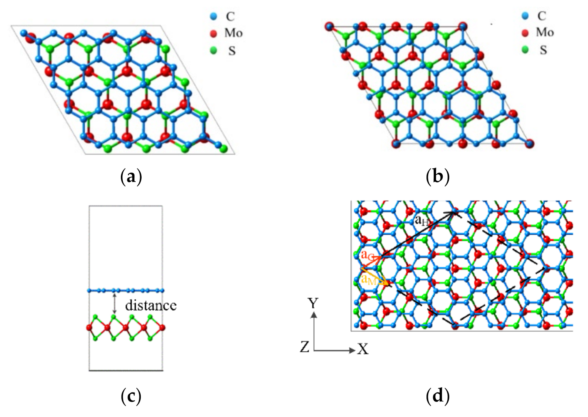
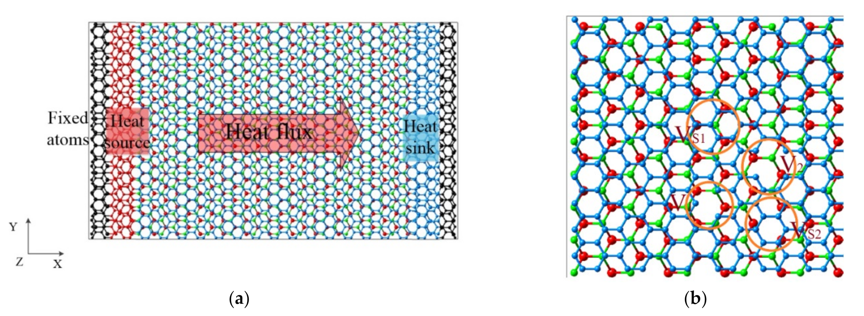
2.2. Molecular Dynamics Simulations

The simulation was performed by the large-scale atomic molecular massively parallel simulator (LAMMPS) package [32]. The optimized Tersoff potentials [33] was adopted to describe C-C interactions in graphene because it can reproduce the correct phonon dispersion and the density of states. We used Stillinger-Weber (SW) potential [34] and SW15 parameters [35], which can accurately describe the thermal and mechanical properties of monolayer MoS2. The 12-6 Lennard-Jones (LJ) potential was adopted to describe van der Waals interactions between graphene and MoS2 atoms:
V ( r ) = 4 χ ε ( σ r ) 12 ( σ r ) 6
where, x, ε, σ, and r are the interface interaction strength, energy parameter, distance parameter, and the distance between the atoms, respectively. In this study, the default setting of x is 1, εMo-C = 1.39 meV, σMo-C = 3.8 Å, εS-C = 7.53 meV, σS-C = 3.22 Å, and r = 1 nm [36].
The non-equilibrium molecular dynamics (NEMD) method was adopted to calculate the heterostructures’ thermal conductivity shown in Figure 2. The length of the rectangle bilayer system is 21.56 nm, and its width is 4.98 nm. Periodic boundary conditions were applied in y- and z- directions. In Figure 2a, the black region with a width of 2.56 Å contains fixed atoms. The left region is the heat source with a width of 1.53 nm, and the blue region is the heat sink with a width of 1.53 nm. Initially, the system equilibrated at a temperature of 300 K, pressure of 1 bar using Nosé-Hoover thermostat under the isothermal-isobaric (NPT) ensemble for 1 ns with the time step of 1 fs. Subsequently, the thermostat was removed and changed into the canonical (NVT) ensemble at a temperature of 300 K for 1 ns. Finally, the system was switched to the microcanonical ensemble for 5 ns. Simultaneously, the Langevin thermostat was applied to maintain heat source temperature at 310 K and heat sink temperature at 290 K. The system equilibrated after 1 ns, and the energy profile was obtained. According to Fourier’s law, the thermal conductivity (K) is obtained by:
K = J A · T X
where, J is the heat flux, A is the cross-sectional area equivalent to width multiplying thickness, and T / X is the temperature gradient in the X direction. In this study, the thickness of the heterostructure is 9.53 Å, which is a sum of monolayer graphene’s thickness of 3.44 Å and monolayer MoS2 thickness of 6.09 Å.
A system with different point defects shown as Figure 2b has also been calculated. The concentration of defect (C) is defined as:
C = N D N G × 100 %
where, ND is the number of defect atoms in graphene or MoS2 layers, NG denoted the total number of atoms in graphene or MoS2, which is 4000 and 3840 in this paper.
The thermal conductance (G) across the graphene/MoS2 interface has been obtained by the thermal relaxation method [37]. Due to its small size and high thermal conductivity, the lumped heat-capacity model can be applied to calculate the thermal conductance (G),
G = C H A τ
where, CH is the effective constant volume heat capacity of the heterostructure. CH can be expressed as
C H = C G C M C G + C M
where, CG and CM are the effective constant volume heat capacity of monolayer graphene and MoS2, which can be written as
C V = i , μ C i , μ = i , μ d k B g i , μ , ( ω ) h ω 2 κ B Τ 2 exp h ω κ B Τ exp h ω κ B Τ 1 2 d ω
where, Ci,μ denoted the contribution of μ atom in i direction to the heat capacity. kB is Boltzmann constant, h is Planck constant, T is temperature in Kelvin, and g(ω) is phonon spectrum power at the frequency ω, which can be expressed as
g ω = 1 2 π e i w t j = 1 N V j t V j 0 d ω
where, Vj(t) is the velocity of the atom j at time t. τ is the relaxation time, which can be calculated by
Δ T t = Δ T t 0 e ( t t 0 ) / τ
where, t0 is origin time, ΔT is the temperature difference between graphene and MoS2. After the system finally reached equilibrium, the graphene was rapidly heated to 500 K by velocity rescaling. The MoS2 layer was still kept at 300 K. The Langevin thermostats were used to maintain graphene at 500 K and MoS2 at 300 K for 1 ns. Finally, the heat baths were removed, and the system reached equilibrium for another 1 ns.

3. Result and Discussion

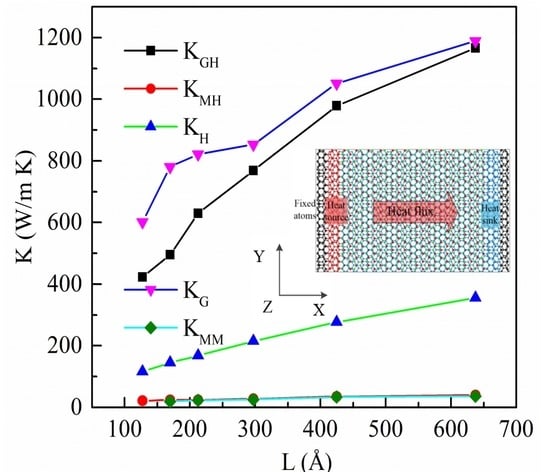
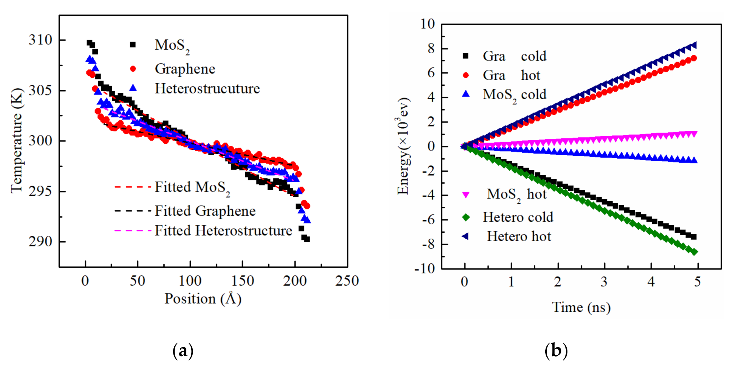
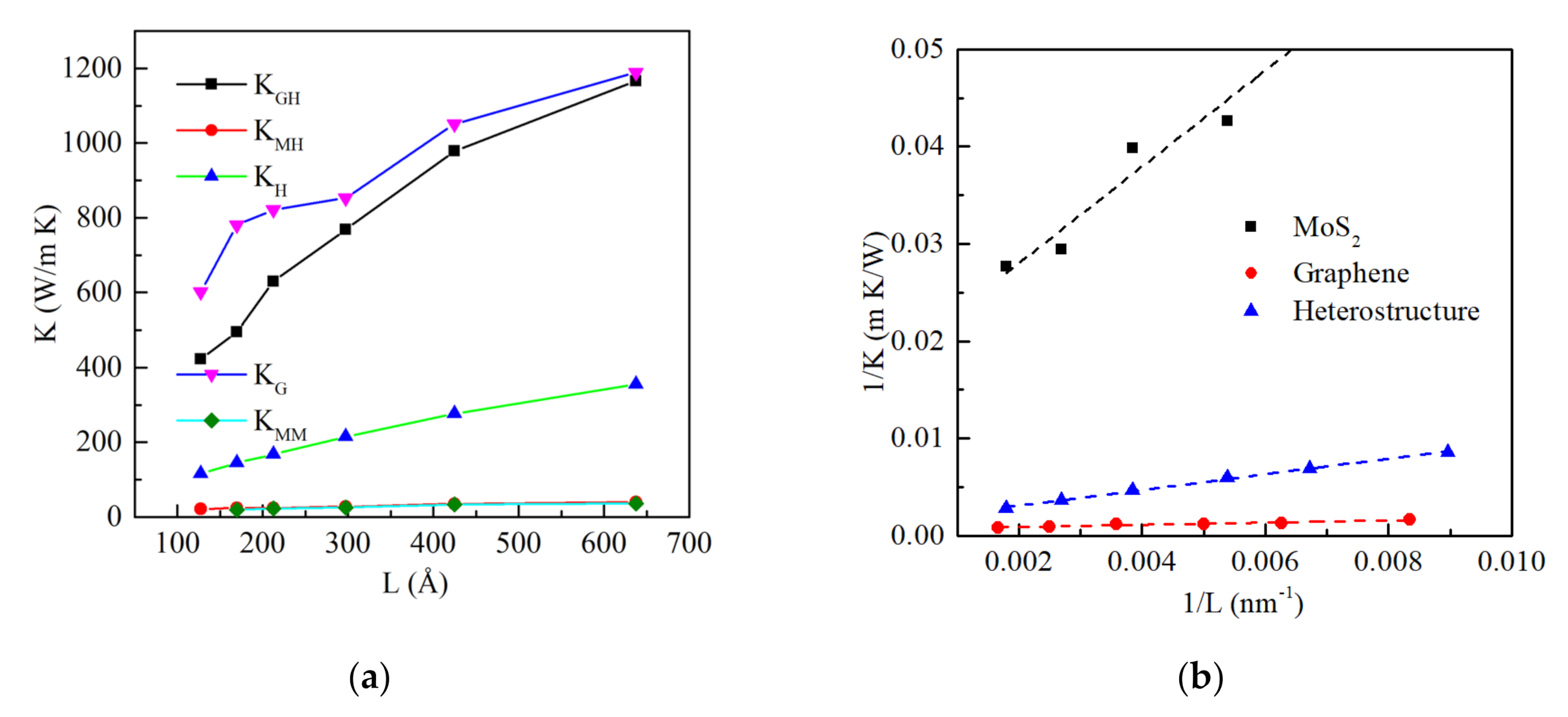
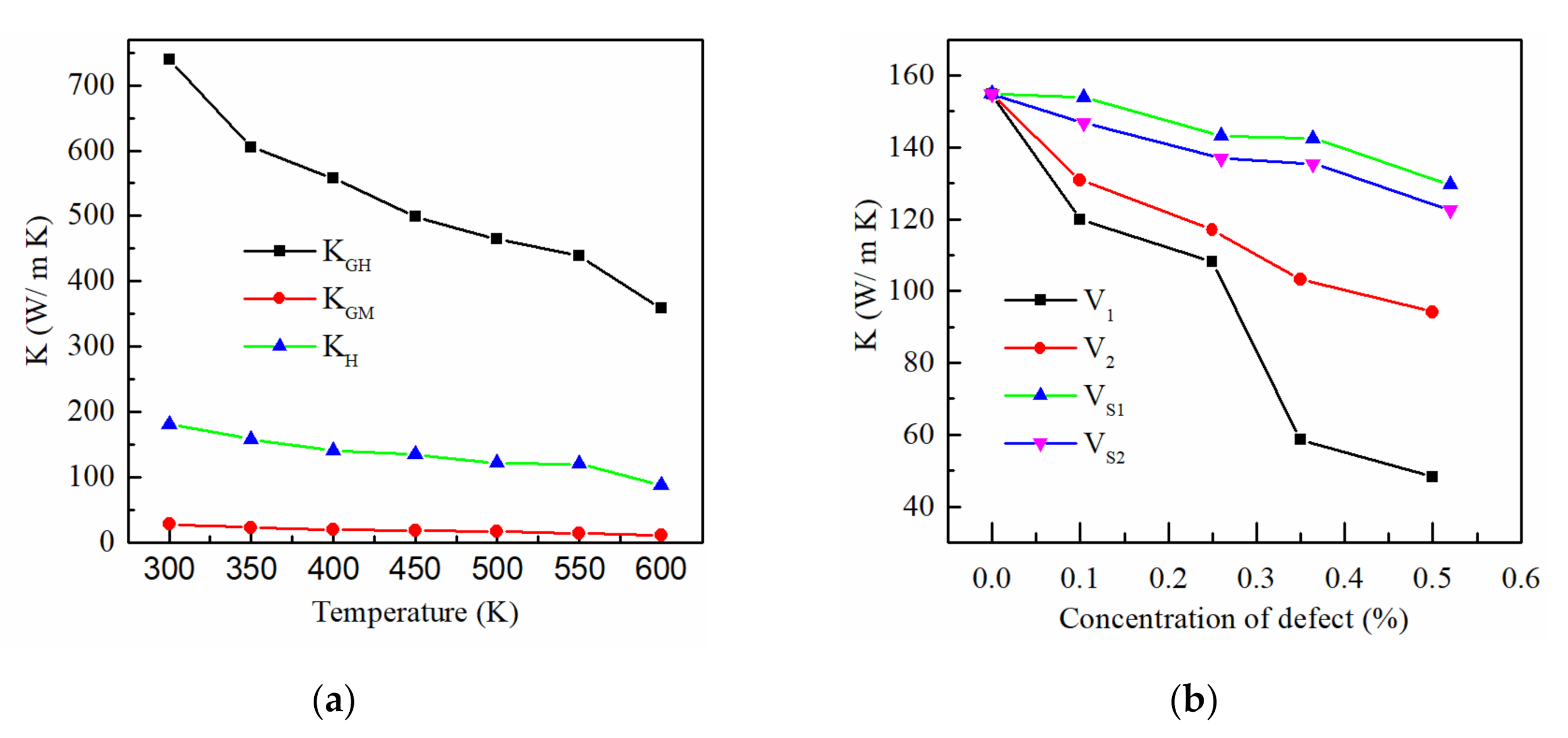
3.1. Thermal Conductivity of the Heterostructure

Figure 3 shows the temperature distribution and energy variation of structure 1, which is stacked in Figure 1a. The heterostructure is nanoribbons with a length (L) of 21.56 nm and width (W) of 4.98 nm. Avoid the heat bathes and boundary effects, the middle part of the system was selected for temperature fitting. The temperature gradients of graphene, MoS2, and graphene/MoS2 bilayer by linear fitting are 0.01902, 0.04633, and 0.03255 K/Å. All the energies subtracted from the heat source and added to the heat sink increase proportionally with the time, as shown in Figure 3b. The energy slope of graphene, MoS2, and total bilayer system are 1482.52, 238.64, and 1721.15 eV/ns, respectively. According to Fourier’s law mentioned above, the thermal conductivities of graphene in the bilayer (KGH), MoS2 in heterostructure (KMH), and the heterostructure are 739.26, 27.6, and 181.03 W/m K, respectively. All the values are lower than 821.28 W/m K, which is the thermal conductivity of monolayer graphene (KG). The result of MoS2 is lower than 34.5 W/m K measured experimentally [38]. Because the phonon mean free path (MFP) of graphene is 775 nm [39], and the simulation model size is much smaller than it. The thermal conductivity of graphene is much lower than 3080–5150 W/m K with a large size [39]. Similar results also can be found in the previous study for the graphene/MoS2/graphene structure [40]. Compared with the free-standing monolayer graphene, the K of heterostructure is significantly decreased for two reasons. One is the bilayer’s area, which is thicker than monolayer graphene. According to Fourier’s law, the area of the system can affect thermal conductivity. Another is that the K of MoS2 is much lower than graphene. In the vdW heterostructure, the thermal transport in MoS2 is much slower than graphene. At the same heat flux, the bilayer system thermal transport is inefficient, so that the thermal conductivity of it is lower than monolayer graphene. For structure 2 stacked as Figure 1b, the KGH, KMH, and KH are 649.89, 21.985, and 154.74 W/m K, respectively. Table 2 presents the comparison of K and G of Graphene/MoS2 obtained in this study with other structures. Since the thermal resistance is actually connected in parallel, the thermal conductivity of heterostructure is lower than that of the monolayer. The higher thermal conductivity materials can transfer more heat, so the K of the vertically stacked heterostructure is higher underlying the same substrate.
The K of heterostructure (116~355 W/m K) with a fixed width of 4.98 nm is lower than that of monolayer graphene (601~1189 W/m K) but higher than that of monolayer MoS2 (19~36 W/m K), as shown in Figure 4a. Because the MFP of MoS2 is about 18.1 nm, both K of monolayer MoS2 and K of the MoS2 in heterostructure change mildly, as shown in Figure 4a. According to the Casimir Limit [50], thermal conductivity values have a strong size dependence. The relation between K−1 and L−1 is depicted in Figure 4b, and the K of the system (infinite length) can obtain by:
1 K = 1 K ( 1 + λ L )
where, λ is MFP and L is the distance between the heat source and heat sink. K of the heterostructure is correlated to be 671.14 W/m K, and the MFP is 539.17 nm that between monolayer graphene and MoS2. K of MoS2 is 55.27 W/m K that approaching the previous 39.8 W/m K, which is the thermal conductivity of armchair monolayer MoS2 with a width fixed at 2 nm [51]. The K of monolayer graphene with width 4.98 nm and infinite-length is 1458.7 W/m K. It is close to 1500 W/m K [52] that is also obtained by applying the optimized Tersoff potentials.
Figure 5a presents the K of graphene, MoS2, and bilayer system at different temperatures. The initial model structure 1 (21.2 nm × 4.9 nm) was simulated. It is observed that all these three thermal conductivities decrease with the temperature. However, the slopes for different structures vary very much. K of graphene decreases very quickly, while K of MoS2 only changes slightly. Because the Debye temperature of graphene is 2100 K [53] and that of MoS2 is 263.2 K, the quantum correction of thermal conductivity is not required in this study. The frequency of phonon increases with temperature, and the phonon collisions increase at the same time. Subsequently, the MFP of graphene gets shorter, and the K of graphene declined obviously. Figure 5b reveals that the defect in the monolayer can affect the K of the bilayer system significantly. The simulation results are for structure 2 (21.5 nm × 4.98 nm), and the styles of single and double point defects are shown in Figure 2b. It clearly shows that the single point vacancy in graphene has the most apparent impact on the thermal conductivity of bilayer. The defects of MoS2 have not many effects because the graphene layer plays a paramount role in the thermal transport of the bilayer. The KH decreases 68.7% when single vacancy concentration is 0.5%, while it only decreases by 39% when double vacancies rise to 0.52%. Because of their less stable two-coordinated atoms, the single vacancies reduce the thermal conductivity much more effectively [54]. The atoms do not follow the normal pattern of vibrations. Thus it causes a higher degree of scattering than double vacancies.

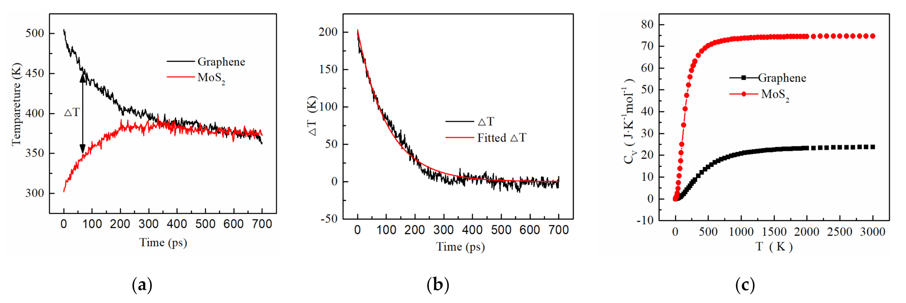
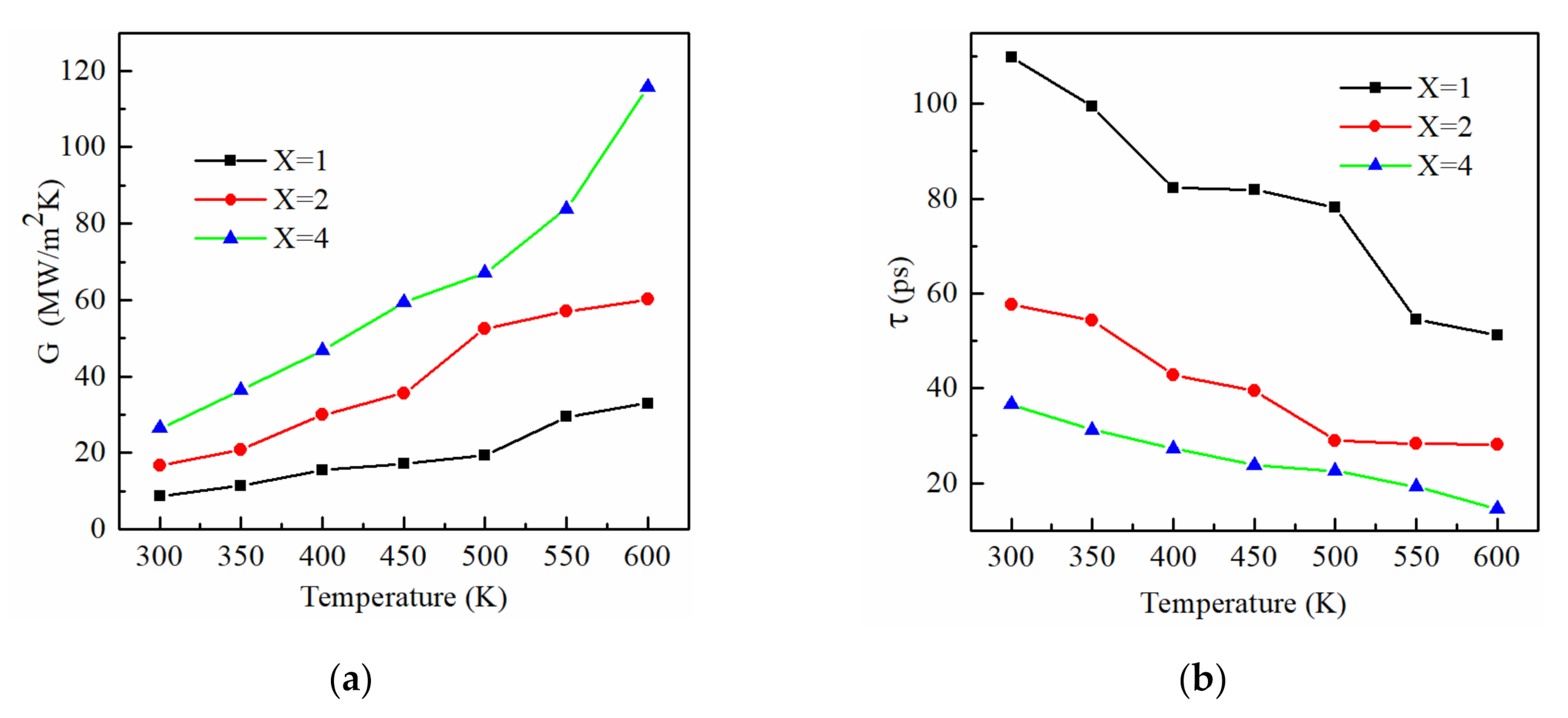
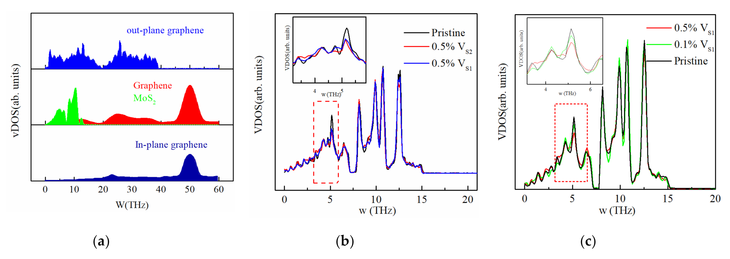
3.2. Thermal Conductance of Graphene/MoS2 Heterostructure

Figure 6a shows the temperature evolution of bilayer after Langevin thermostats were removed. By nonlinear fitting, Δ T = 203.16 e t / 108.02 for the initial structure 1 stacked as Figure 1a shown. For structure 2, τ can be obtained as 105.04 ps. CH at temperature 300 K is 7.74 J·K−1 mol−1 that can be calculated from Figure 6c. So the thermal conductance of graphene/MoS2 is 8.95 MW/m2·K for model 1 and 9.2 MW/m2·K for the other model. It is found that the initial model has little effect on thermal conductance. That is higher than previous investigations on the thermal conductance of the bilayer graphene/MoS2 system, which is 5.8 MW/m2·K [49]. Moreover it is lower than of graphene/MoS2 (13.8 MW/m2·K) [25] and higher than that of monolayer MoS2 on the Au substrate (0.44 MW/m2·K) [55].
Figure 7 presents the temperature and coupling strength (X) dependent interface thermal conductance. From the mentioned equation of thermal conductance above, the CH and τ would have a similar effect. For X = 1, the CH of bilayer changes 74.38% when T is increased from 300 to 600 K. The G increases 274.1%, and τ decreases 53.38% at the same time. When the X is increased by a factor of four, G increases 200.1%, and τ decreases 66.67% at temperature 300 K. To better understand the K of the heterostructure with different defects, the vibrational phonon density of states (vDOS) of graphene and MoS2 in heterostructure have been calculated, and the results for different conditions are shown in Figure 8.
It can be observed in Figure 8a that the overlapped region of graphene and MoS2 are mostly in the frequency range from 1 THz up to 15 THz. The low-frequency phonons in graphene (out-plane) and MoS2 play a significant role in thermal transport. These phonons can provide more channels for phonon transport, and lower frequency phonons transport most heat in the bilayer system. When the temperature rises, most phonons are excited, and Umklapp scattering is enhanced at the same time. More channels are provided, and the relaxation time τ is decreased, so the G increases with the temperature. When X increases, the efficiency of thermal transport is improved, and the G would be enhanced [49]. At the same time, the phonon in the MoS2 layer can be much easier obtained from out-plane graphene to in-plane graphene, and the thermal transport between layers is enhanced. The interface thermal conductance would be increased as a consequence of it.
The vDOS of MoS2 with different defects shown in Figure 8b,c are obtained to explain their effect on the thermal conductivity in detail. The vDOS of MoS2 with VS1 or VS2 point vacancy is very close to pristine MoS2. It can be observed in the enlarged box in Figure 8b that the vDOS of MoS2 with Vs2 is slightly less than that of VS1. Therefore, the KH is little changed, and VS1 vacancy in MoS2 has little influence on KH, as shown in Figure 5b. With the concentration of defect increasing, the DOS of phonon in MoS2 is decreased, and the vibrational modes are suppressed. Hence the relaxation time and phonon MFP decrease at the same time. The K of the system decreases with the concentration of vacancy. It has less influence on KH than graphene owing to the relatively minor role played in thermal transports.
The phonon spectra shown in Figure 9 are obtained by the GULP [56]. The optimized Tersoff and SW potentials have been used to describe the interaction force. In Figure 9, the maximum wavenumber of monolayer graphene is around 50 THZ, and that of MoS2 is around 15 THZ. This result has also been reflected in Figure 8, where the phonon density states of graphene are located in the high frequency around 50 THZ, and that of MoS2 cut off at around15 THZ. Along Г to M direction in Figure 9, the TA, LA, and TO branches of graphene cut off at around 36 THZ, and the ZO and ZA branch cut off at around 21 THZ, corresponding to the PDOS of graphene shown in Figure 8a. The ZA, TA, and LA branches of MoS2 cut off at around 5 THZ along Г to M direction, so the enlarged area of PDOS shown in Figure 8b, c is selected from 4 THZ to 6 THZ. The results also show that the lower frequency phonons play a major role in thermal transport, which can also be found in Figure 8.

4. Conclusions

In this study, graphene/MoS2 heterostructures have been established and optimized by density functional theory. A non-equilibrium molecular dynamics simulation method was applied to calculate the thermal conductivity and interfacial thermal conductance of the bilayer system. The results showed that KH increases with length, and the K of infinitely long graphene/MoS2 (width = 4.98 nm) has been obtained to be 671.14 W/m K. The influencing factors of KH also have been analyzed carefully. It is revealed that KH increases with the temperature and the concentration of defect contained. The single vacancy in graphene can significantly decrease the KH. The thermal conductance of the heterostructure has been found to be 8.95 MW/m2·K, which is much higher than that of MoS2 on the substrate. Finally, the vDOS and phonon spectra of graphene and MoS2 have been further analyzed for a better understanding of the affecting factors on G and K. The out-plane phonons in graphene transport most thermal energy. The increasing coupling strength X and temperature can improve thermal conductance.

Author Contributions

Conceptualization, J.W. and H.X.; data curation, S.W.; formal analysis, S.W., J.W. and Z.G.; investigation, J.W.; methodology, J.W.; resources, H.X.; software, S.W., J.W. and Z.G.; writing—original draft, S.W.; writing—review and editing, J.W., H.X. and Z.G. All authors have read and agreed to the published version of the manuscript.

Funding

This work was supported by the National Natural Science Foundation of China (No. 51776116); The Major Program of the National Natural Science Foundation of China (No. 51590902); Gaoyuan Discipline of Shanghai—Environmental Science and Engineering (Resource Recycling Science and Engineering).

Conflicts of Interest

The authors declare no conflict of interest.

References

  1. Tries, A.; Osella, S.; Zhang, P.; Xu, F.; Ramanan, C.; Klaui, M.; Mai, Y.; Beljonne, D.; Wang, H.I. Experimental Observation of Strong Exciton Effects in Graphene Nanoribbons. Nano Lett. 2020, 20, 2993–3002. [Google Scholar] [CrossRef] [PubMed] [Green Version]
  2. Bouzerar, G.; Thebaud, S.; Pecorario, S.; Adessi, C. Drastic effects of vacancies on phonon lifetime and thermal conductivity in graphene. J. Phys. Condes. Matter 2020, 32, 295702. [Google Scholar] [CrossRef] [PubMed]
  3. Cao, K.; Feng, S.Z.; Han, Y.; Gao, L.B.; Ly, T.H.; Xu, Z.P.; Lu, Y. Elastic straining of free-standing monolayer graphene. Nat. Commun. 2020, 11, 284. [Google Scholar] [CrossRef] [PubMed] [Green Version]
  4. Wang, B.; Ruan, T.T.; Chen, Y.; Jin, F.; Peng, L.; Zhou, Y.; Wang, D.L.; Dou, S.X. Graphene-based composites for electrochemical energy storage. Energy Storage Mater. 2020, 24, 22–51. [Google Scholar] [CrossRef]
  5. Oh, S.; Kim, C.K.; Kim, J. High Responsivity beta-Ga2O3 Metal-Semiconductor-Metal Solar-Blind Photodetectors with Ultraviolet Transparent Graphene Electrodes. ACS Photonics 2018, 5, 1123–1128. [Google Scholar] [CrossRef]
  6. Li, B.; Luo, J.C.; Huang, X.W.; Lin, L.W.; Wang, L.; Hu, M.J.; Tang, L.C.; Xue, H.G.; Gao, J.F.; Mai, Y.W. A highly stretchable, super-hydrophobic strain sensor based on polydopamine and graphene reinforced nanofiber composite for human motion monitoring. Compos. Pt. B Eng. 2020, 181, 107580. [Google Scholar] [CrossRef]
  7. Gupta, U.; Rao, C.N.R. Hydrogen generation by water splitting using MoS2 and other transition metal dichalcogenides. Nano Energy 2017, 41, 49–65. [Google Scholar] [CrossRef]
  8. Ma, S.N.; Chiu, C.P.; Zhu, Y.J.; Tang, C.Y.; Long, H.; Qarony, W.; Zhao, X.H.; Zhang, X.M.; Lo, W.H.; Tsang, Y.H. Recycled waste black polyurethane sponges for solar vapor generation and distillation. Appl. Energy 2017, 206, 63–69. [Google Scholar] [CrossRef]
  9. Frisenda, R.; Navarro-Moratalla, E.; Gant, P.; De Lara, D.P.; Jarillo-Herrero, P.; Gorbachev, R.V.; Castellanos-Gomez, A. Recent progress in the assembly of nanodevices and van der Waals heterostructures by deterministic placement of 2D materials. Chem. Soc. Rev. 2018, 47, 53–68. [Google Scholar] [CrossRef] [PubMed] [Green Version]
  10. Li, X.W.; Huang, C.W.; Hu, S.B.; Deng, B.; Chen, Z.H.; Han, W.Q.; Chen, L. Negative and near-zero Poisson’s ratios in 2D graphene/MoS2 and graphene/h-BN heterostructures. J. Mater. Chem. C 2020, 8, 4021–4029. [Google Scholar] [CrossRef]
  11. Ren, K.; Sun, M.L.; Luo, Y.; Wan, S.K.; Yu, J.; Tang, W.C. First-principle study of electronic and optical properties of two-dimensional materials-based heterostructures based on transition metal dichalcogenides and boron phosphide. Appl. Surf. Sci. 2019, 476, 70–75. [Google Scholar] [CrossRef]
  12. Chen, Y.; Wang, X.D.; Wu, G.J.; Wang, Z.; Fang, H.H.; Lin, T.; Sun, S.; Shen, H.; Hu, W.D.; Wang, J.L.; et al. High-Performance Photovoltaic Detector Based on MoTe2/MoS2 Van der Waals Heterostructure. Small 2018, 14, 1703293. [Google Scholar] [CrossRef] [PubMed]
  13. Li, G.; Zhang, L.Z.; Xu, W.Y.; Pan, J.B.; Song, S.R.; Zhang, Y.; Zhou, H.T.; Wang, Y.L.; Bao, L.H.; Zhang, Y.Y.; et al. Stable Silicene in Graphene/Silicene Van der Waals Heterostructures. Adv. Mater. 2018, 30, 1804650. [Google Scholar] [CrossRef]
  14. Biroju, R.K.; Das, D.; Sharma, R.; Pal, S.; Mawlong, L.P.L.; Bhorkar, K.; Giri, P.K.; Singh, A.K.; Narayanan, T.N. Hydrogen Evolution Reaction Activity of Graphene-MoS2 van der Waals Heterostructures. ACS Energy Lett. 2017, 2, 1355–1361. [Google Scholar] [CrossRef]
  15. Safeer, C.K.; Ingla-Aynes, J.; Herling, F.; Garcia, J.H.; Vila, M.; Ontoso, N.; Calvo, M.R.; Roche, S.; Hueso, L.E.; Casanova, F. Room-Temperature Spin Hall Effect in Graphene/MoS2 van der Waals Heterostructures. Nano Lett. 2019, 19, 1074–1082. [Google Scholar] [CrossRef] [Green Version]
  16. Sun, X.L.; Zhang, B.T.; Li, Y.L.; Luo, X.Y.; Li, G.R.; Chen, Y.X.; Zhang, C.Q.; He, J.L. Tunable Ultrafast Nonlinear Optical Properties of Graphene/MoS2 van der Waals Heterostructures and Their Application in Solid-State Bulk Lasers. ACS Nano 2018, 12, 11376–11385. [Google Scholar] [CrossRef]
  17. Gong, F.; Ding, Z.W.; Fang, Y.; Tong, C.J.; Xia, D.W.; Lv, Y.Y.; Wang, B.; Papavassiliou, D.V.; Liao, J.X.; Wu, M.Q. Enhanced Electrochemical and Thermal Transport Properties of Graphene/MoS2 Heterostructures for Energy Storage: Insights from Multiscale Modeling. ACS Appl. Mater. Interfaces 2018, 10, 14614–14621. [Google Scholar] [CrossRef] [PubMed]
  18. Zhang, Z.W.; Xie, Y.E.; Peng, Q.; Chen, Y.P. Thermal transport in MoS2/Graphene hybrid nanosheets. Nanotechnology 2015, 26, 375402. [Google Scholar] [CrossRef] [Green Version]
  19. Oh, J.; Kim, Y.; Chung, S.; Kim, H.; Son, J.G. Fabrication of a MoS2/Graphene Nanoribbon Heterojunction Network for Improved Thermoelectric Properties. Adv. Mater. Interfaces 2019, 6, 1901333. [Google Scholar] [CrossRef]
  20. Kresse, G.; Furthmuller, J. Efficient iterative schemes for ab initio total-energy calculations using a plane-wave basis set. Phys. Rev. B 1996, 54, 11169–11186. [Google Scholar] [CrossRef]
  21. Perdew, J.P.; Burke, K.; Ernzerhof, M. Generalized gradient approximation made simple. Phys. Rev. Lett. 1996, 77, 3865–3868. [Google Scholar] [CrossRef] [PubMed] [Green Version]
  22. Grimme, S. Semiempirical GGA-type density functional constructed with a long-range dispersion correction. J. Comput. Chem. 2006, 27, 1787–1799. [Google Scholar] [CrossRef] [PubMed]
  23. Ma, Y.D.; Dai, Y.; Guo, M.; Niu, C.W.; Huang, B.B. Graphene adhesion on MoS2 monolayer: An ab initio study. Nanoscale 2011, 3, 3883–3887. [Google Scholar] [CrossRef]
  24. Qiu, B.; Zhao, X.W.; Hu, G.C.; Yue, W.W.; Ren, J.F.; Yuan, X.B. Optical Properties of Graphene/MoS2 Heterostructure: First Principles Calculations. Nanomaterials 2018, 8, 962. [Google Scholar] [CrossRef] [Green Version]
  25. Ding, Z.W.; Pei, Q.X.; Jiang, J.W.; Huang, W.X.; Zhang, Y.W. Interfacial thermal conductance in graphene/MoS2 heterostructures. Carbon 2016, 96, 888–896. [Google Scholar] [CrossRef]
  26. Nakamura, H.; Mohammed, A.; Rosenzweig, P.; Matsuda, K.; Nowakowski, K.; Kuster, K.; Wochner, P.; Ibrahimkutty, S.; Wedig, U.; Hussain, H.; et al. Spin splitting and strain in epitaxial monolayer WSe2 on graphene. Phys. Rev. B 2020, 101, 8. [Google Scholar] [CrossRef] [Green Version]
  27. Naumov, N.G.; Korlyukov, A.A.; Piryazev, D.A.; Virovets, A.V.; Fedorov, V.E. High-precision X-ray diffraction data, experimental and theoretical study of 2H-MoS2. Russ. Chem. Bull. 2013, 62, 1852–1857. [Google Scholar] [CrossRef]
  28. Tornatzky, H.; Gillen, R.; Uchiyama, H.; Maultzsch, J. Phonon dispersion in MoS. Phys. Rev. B 2019, 99, 144309. [Google Scholar] [CrossRef] [Green Version]
  29. Schumann, T.; Dubslaff, M.; Oliveira, M.H.; Hanke, M.; Lopes, J.M.J.; Riechert, H. Effect of buffer layer coupling on the lattice parameter of epitaxial graphene on SiC(0001). Phys. Rev. B 2014, 90, 5. [Google Scholar] [CrossRef] [Green Version]
  30. Phuc, H.V.; Hieu, N.N.; Hoi, B.D.; Phuong, L.T.T.; Nguyen, C.V. First principle study on the electronic properties and Schottky contact of graphene adsorbed on MoS2 monolayer under applied out-plane strain. Surf. Sci. 2018, 668, 23–28. [Google Scholar] [CrossRef]
  31. Jin, C.J.; Rasmussen, F.A.; Thygesen, K.S. Tuning the Schottky Barrier at the Graphene/MoS2 Interface by Electron Doping: Density Functional Theory and Many-Body Calculations. J. Phys. Chem. C 2015, 119, 19928–19933. [Google Scholar] [CrossRef]
  32. Plimpton, S. Fast parallel algorithms for short-range molecular dynamics. J. Comput. Phys. 1995, 117, 1–19. [Google Scholar] [CrossRef] [Green Version]
  33. Lindsay, L.; Broido, D.J.P.R.B. Optimized Tersoff and Brenner empirical potential parameters for lattice dynamics and phonon thermal transport in carbon nanotubes and graphene. Phys. Rev. B 2010, 81, 205441. [Google Scholar] [CrossRef] [Green Version]
  34. Stillinger, W. Computer simulation of local order in condensed phases of silicon. Phys. Rev. B Condens. Matter 1985, 31, 5262–5271. [Google Scholar] [CrossRef] [Green Version]
  35. Jiang, J.W. Parametrization of Stillinger-Weber potential based on valence force field model: Application to single-layer MoS2 and black phosphorus. Nanotechnology 2015, 26, 315706. [Google Scholar] [CrossRef] [Green Version]
  36. Vazirisereshk, M.R.; Ye, H.; Ye, Z.J.; Otero-de-la-Roza, A.; Zhao, M.Q.; Gao, Z.L.; Johnson, A.T.C.; Johnson, E.R.; Carpick, R.W.; Martini, A. Origin of Nanoscale Friction Contrast between Supported Graphene, MoS2, and a Graphene/MoS2 Heterostructure. Nano Lett. 2019, 19, 5496–5505. [Google Scholar] [CrossRef]
  37. Liu, B.; Baimova, J.A.; Reddy, C.D.; Law, A.W.K.; Dmitriev, S.V.; Wu, H.; Zhou, K. Interfacial Thermal Conductance of a Silicene/Graphene Bilayer Heterostructure and the Effect of Hydrogenation. ACS Appl. Mater. Interfaces 2014, 6, 18180–18188. [Google Scholar] [CrossRef]
  38. Yan, R.S.; Simpson, J.R.; Bertolazzi, S.; Brivio, J.; Watson, M.; Wu, X.F.; Kis, A.; Luo, T.F.; Walker, A.R.H.; Xing, H.G. Thermal Conductivity of Monolayer Molybdenum Disulfide Obtained from Temperature-Dependent Raman Spectroscopy. ACS Nano 2014, 8, 986–993. [Google Scholar] [CrossRef]
  39. Ghosh, S.; Calizo, I.; Teweldebrhan, D.; Pokatilov, E.P.; Nika, D.L.; Balandin, A.A.; Bao, W.; Miao, F.; Lau, C.N. Extremely high thermal conductivity of graphene: Prospects for thermal management applications in nanoelectronic circuits. Appl. Phys. Lett. 2008, 92, 151911. [Google Scholar] [CrossRef]
  40. Srinivasan, S.; Balasubramanian, G. Reduced Thermal Transport in the Graphene/MoS2/Graphene Heterostructure: A Comparison with Freestanding Monolayers. Langmuir 2018, 34, 3326–3335. [Google Scholar] [CrossRef]
  41. Chen, Y.; Zhang, Y.Y.; Cai, K.; Jiang, J.W.; Zheng, J.C.; Zhao, J.H.; Wei, N. Interfacial thermal conductance in graphene/black phosphorus heterogeneous structures. Carbon 2017, 117, 399–410. [Google Scholar] [CrossRef] [Green Version]
  42. Liu, Y.; Ong, Z.Y.; Wu, J.; Zhao, Y.S.; Watanabe, K.; Taniguchi, T.; Chi, D.Z.; Zhang, G.; Thong, J.T.L.; Qiu, C.W.; et al. Thermal Conductance of the 2D MoS2/h-BN and graphene/h-BN Interfaces. Sci Rep. 2017, 7, 8. [Google Scholar] [CrossRef] [PubMed] [Green Version]
  43. Yu, Y.F.; Minhaj, T.; Huang, L.J.; Yu, Y.L.; Cao, L.Y. In-Plane and Interfacial Thermal Conduction of Two-Dimensional Transition-Metal Dichalcogenides. Phys. Rev. Appl. 2020, 13, 034059. [Google Scholar] [CrossRef]
  44. Rahman, M.; Shahzadeh, M.; Pisana, S. Simultaneous measurement of anisotropic thermal conductivity and thermal boundary conductance of 2-dimensional materials. J. Appl. Phys. 2019, 126, 205103. [Google Scholar] [CrossRef]
  45. Wu, Y.J.; Lan, Y.W.; Hsu, S.C.; Yeh, C.H.; Ku, Y.S.; Jiang, J.C.; Xu, Y.B. Tuning Interfacial Thermal and Electrical Conductance across a Metal/MoS2 Monolayer through N-Methyl-2-pyrrolidone Wet Cleaning. Adv. Mater. Interfaces 2020, 2000364. [Google Scholar] [CrossRef]
  46. Aiyiti, A.; Bai, X.; Wu, J.; Xu, X.F.; Li, B.W. Measuring the thermal conductivity and interfacial thermal resistance of suspended MoS2 using electron beam self-heating technique. Sci. Bull. 2018, 63, 452–458. [Google Scholar] [CrossRef] [Green Version]
  47. Zheng, X.Z.; Zhao, C.Y.; Gu, X.K. Thermal conductivity of MoS2/MoSe2 heterostructures: The role of lattice mismatch, interlayer rotation and species intermixing. Int. J. Heat Mass Transf. 2019, 143, 118583. [Google Scholar] [CrossRef]
  48. Hong, Y.; Ju, M.G.; Zhang, J.C.; Zeng, X.C. Phonon thermal transport in a graphene/MoSe2 van der Waals heterobilayer. Phys. Chem. Chem. Phys. 2018, 20, 2637–2645. [Google Scholar] [CrossRef]
  49. Liu, B.; Meng, F.M.; Reddy, C.D.; Baimova, J.A.; Srikanth, N.; Dmitriev, S.V.; Zhou, K. Thermal transport in a graphene-MoS2 bilayer heterostructure: A molecular dynamics study. RSC Adv. 2015, 5, 29193–29200. [Google Scholar] [CrossRef]
  50. Casimir, H.B.G. Note on the Conduction of Heat in Crystals. Physica 1938, 5, 495–500. [Google Scholar] [CrossRef]
  51. Zhang, C.; Wang, C.X.; Rabczuk, T. Thermal conductivity of single-layer MoS2: A comparative study between 1H and 1T′ phases. Physica E 2018, 103, 294–299. [Google Scholar] [CrossRef]
  52. Cao, A.J.; Qu, J.M. Kapitza conductance of symmetric tilt grain boundaries in graphene. J. Appl. Phys. 2012, 111, 053529. [Google Scholar] [CrossRef]
  53. Pop, E.; Varshney, V.; Roy, A.K. Thermal properties of graphene: Fundamentals and applications. MRS Bull. 2012, 37, 1273–1281. [Google Scholar] [CrossRef] [Green Version]
  54. Haskins, J.; Kinaci, A.; Sevik, C.; Sevincli, H.; Cuniberti, G.; Cagin, T. Control of Thermal and Electronic Transport in Defect-Engineered Graphene Nanoribbons. ACS Nano 2011, 5, 3779–3787. [Google Scholar] [CrossRef]
  55. Zhang, X.; Sun, D.Z.; Li, Y.L.; Lee, G.H.; Cui, X.; Chenet, D.; You, Y.M.; Heinz, T.F.; Hone, J.C. Measurement of Lateral and Interfacial Thermal Conductivity of Single- and Bilayer MoS2 and MoSe2 Using Refined Optothermal Raman Technique. ACS Appl. Mater. Interfaces 2015, 7, 25923–25929. [Google Scholar] [CrossRef] [PubMed] [Green Version]
  56. Gale, J.D.; Rohl, A.L. The General Utility Lattice Program (GULP). Mol. Simul. 2003, 29, 291–341. [Google Scholar] [CrossRef]
Figure 1. Graphene/MoS2 heterostructure. (a) Top view of structure 1 (b) top view of structure 2 (c) side view of structure 2 (d) top view of the heterostructure, the black parallelogram represents the Bravais lattice (structure 2 in the supercell).
Energies 13 05851 g001
Figure 2. (a) Schematic for NEMD of graphene/MoS2 rectangle heterostructure model, (b) point defect in heterostructure. V1 is single vacancy graphene; V2 is double vacancies in graphene; VS1 is single S atom vacancy in Z direction; VS2 vacancy with two S atoms in MoS2.
Energies 13 05851 g002
Figure 3. (a) Temperature distribution of graphene/MoS2 heterostructure in the structure 1, (b) accumulation of input and output energy of structure 1.
Energies 13 05851 g003
Figure 4. (a) Thermal conductivity (K) of graphene/MoS2 bilayer (KGM), monolayer grapheme (KG), MoS2 (KMM), graphene (KGH) and MoS2 (KMH) in bilayer as a function of the sample length (L) (b) K−1 as function of L−1 for graphene/MoS2 heterostructure, graphene, and MoS2 monolayer.
Energies 13 05851 g004
Figure 5. (a) Temperature dependence of KH, KMH, and KGH, and (b) thermal conductivity of heterostructure as a function of defect concentration.
Energies 13 05851 g005
Figure 6. (a) Temperature profile of graphene and MoS2 in the heterostructure, (b) temperature difference between layers as a function of relaxation time, and (c) effective constant volume heat capacity of monolayer graphene and MoS2 at different temperatures.
Energies 13 05851 g006
Figure 7. (a) Interface thermal conductance at different temperatures and coupling strength (X) between layers, (b) the relaxation time τ at different temperatures.
Energies 13 05851 g007
Figure 8. vDOS of graphene and MoS2 in bilayer system (a) total, out-plane and in-plane phonon DOS (PDOS) of graphene and MoS2, (b) different MoS2 defect types at 0.5% defect concentration, (c) same MoS2 defect types at different concentration.
Energies 13 05851 g008
Figure 9. (a) Phonon spectra of monolayer graphene, (b) monolayer MoS2.
Energies 13 05851 g009
Table 1. The lattice constant of graphene and MoS2 in this work and previous studies.
Ref.MaterialsMethodLattice Constant a (Å)
Ma et al. [23]Monolayer grapheneFirst-principlesa = 2.45
Monolayer MoS2a = 3.12
Qin et al. [24]Monolayer grapheneFirst-principlesa = 2.47
Monolayer MoS2a = 3.16
Ding et al. [25]Monolayer grapheneFirst-principlesa = 2.49
Monolayer MoS2a = 3.12
Nakamura [26]Graphene beneath WSe2Experimenta = 2.4575 ± 0.0007
Tornatzky [27]Multilayer MoS2Experimenta = 3.161
Bilayer MoS2First-principlesa = 3.158
Naumov [28]Multilayer MoS2Experimenta = 3.16
Schumann [29]Bilayer grapheneExperimenta = 2.467
Monolayer graphene/Bilayer graphenea = 2.456/2.463
This workMonolayer grapheneFirst-principlesa = 2.45/2.47
Monolayer MoS2a = 3.12/3.16
Table 2. Thermal conductivity (K) and interface thermal conductance (G) of heterostructure from previous MD simulation and experiment.
Ref.MaterialsMethodTemperature (K)K (W/m K)G (MW/m2 K)
Srinivasan et al. [40]graphene/MoS2/grapheneMD30017–650.76–0.9
Chen et al. [41]BP/grapheneMD100–350 25.33–56.34
Liu et al. [42]MoS2/h-BN
graphene/h-BN
ExperimentRoom temperature 17 ± 0.4
52.2 ± 2.1
Yu et al. [43]MoS2/SiO2ExperimentRoom temperature32.5 ± 3.418.6
Rahuman et al. [44]graphene/SiO2
MoS2/SiO2
ExperimentRoom temperature636 ± 140
63 ± 22
Wu et al. [45]Au/MoS2ExperimentRoom temperature 5.12
Aiyiti et al. [46]MoS2/ptExperimentRoom temperature300.5
Zheng et al. [47]MoS2/MoSe2MD30017.48
Hong et al. [48]graphene/MoSe2MD300138.245.26
Liu et al. [49]graphene/MoS2MD35031.745.81
Publisher’s Note: MDPI stays neutral with regard to jurisdictional claims in published maps and institutional affiliations.

