
Design of a Current Sensing System with TIA Gain of 160 dBΩ and Input-Referred Noise of 1.8 pArms for Biosensor
 ,
,  ,
,
Abstract
:1. Introduction
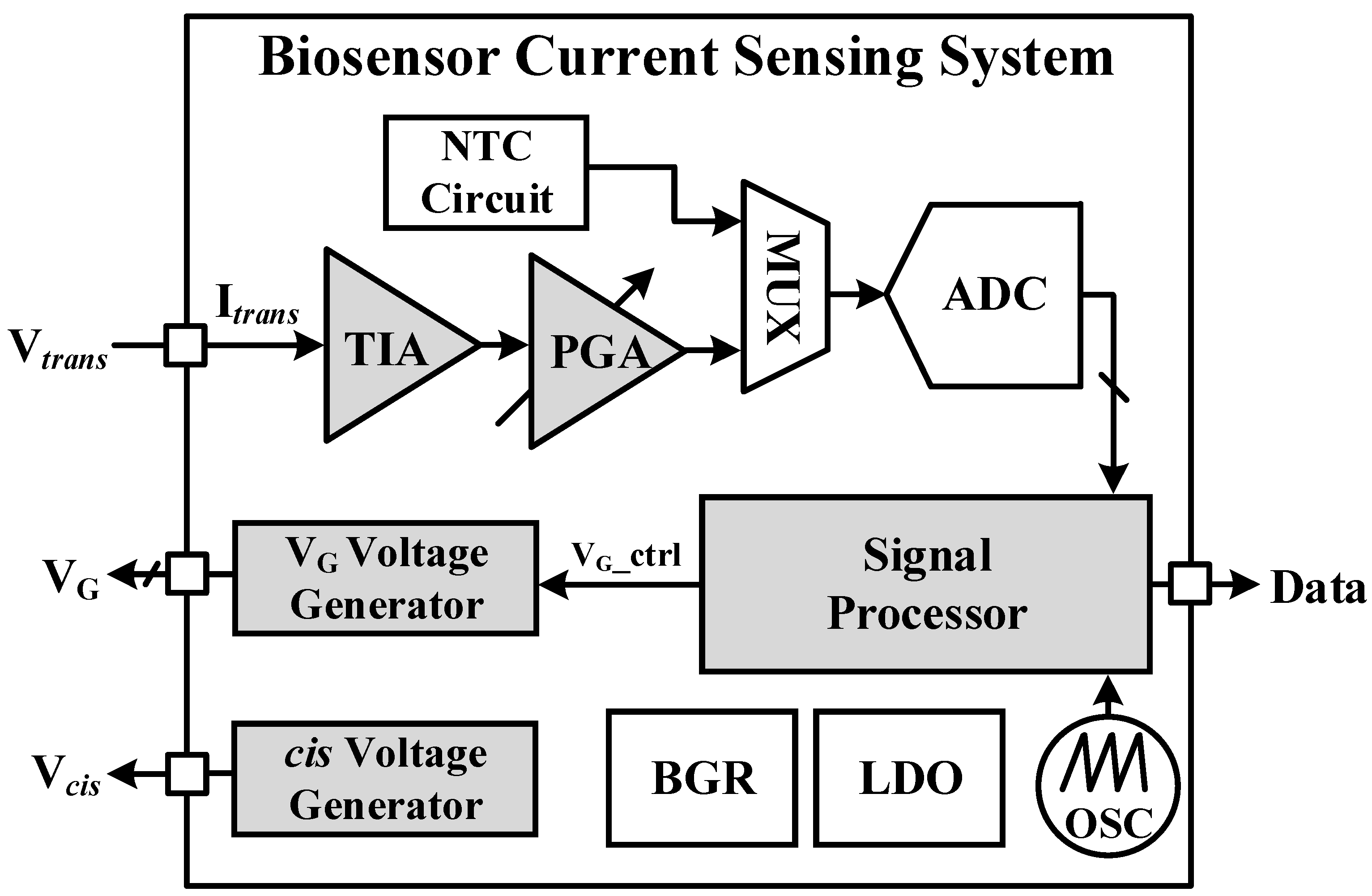
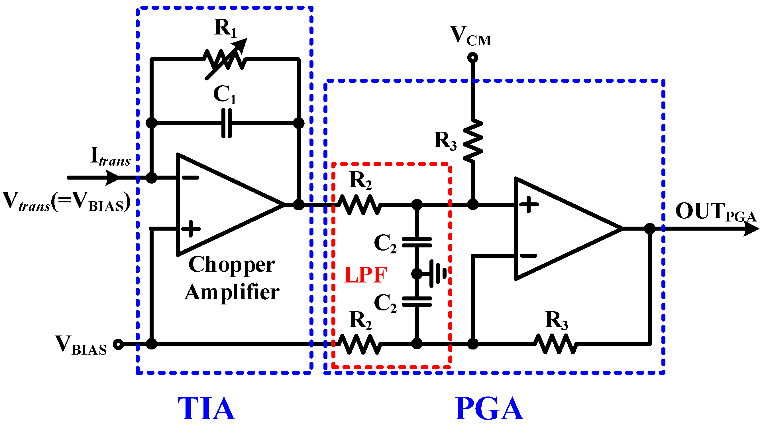
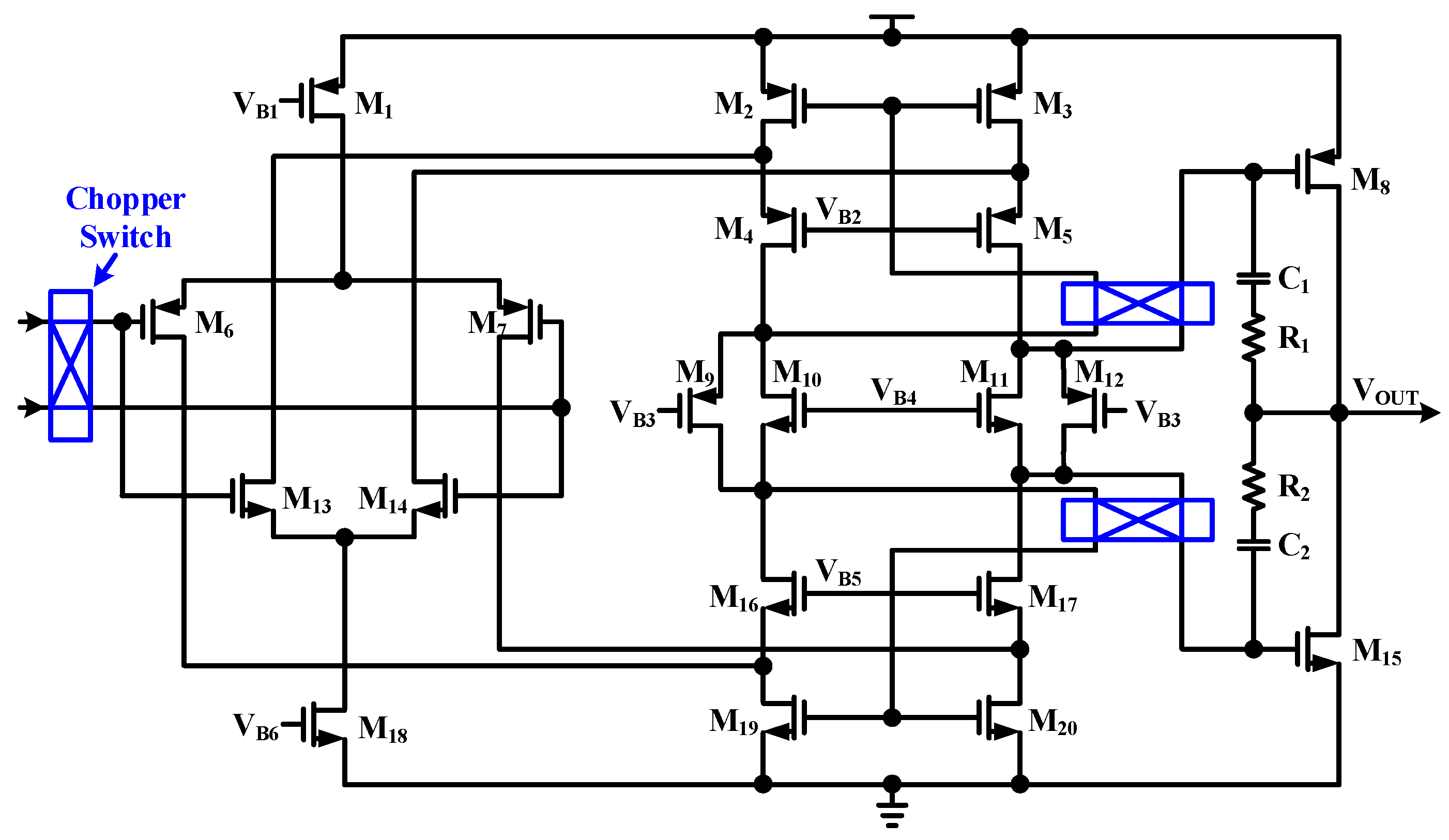
2. The Proposed Current Sensing System
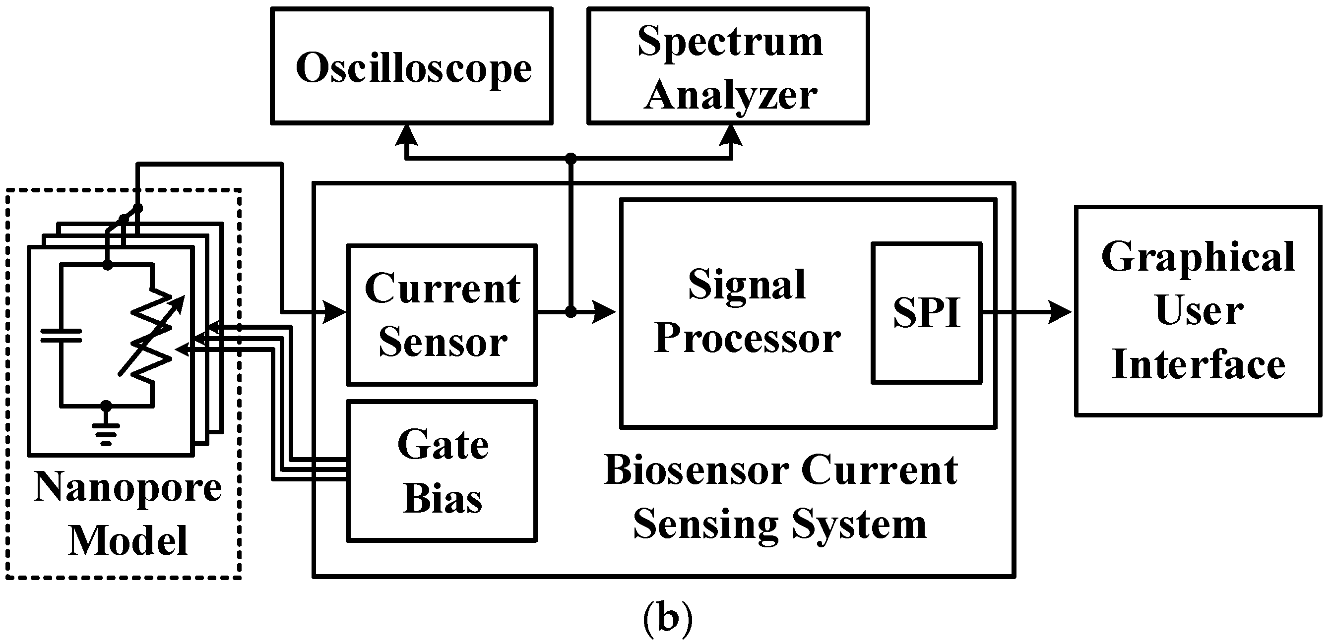
3. Experimental Results
4. Conclusions
Author Contributions
Funding
Institutional Review Board Statement
Informed Consent Statement
Data Availability Statement
Conflicts of Interest
References
- Goud, K.Y.; Moonla, C.; Mishra, R.K.; Yu, C.; Narayan, R.; Litvan, I.; Wang, J. Wearable electrochemical microneedle sensor for continuous monitoring of levodopa: Toward parkinson management. ACS Sens. 2019, 4, 2196–2204. [Google Scholar] [CrossRef] [PubMed]
- Zhang, Z.; Li, M.; Zuo, Y.; Chen, S.; Zhuo, Y.; Lu, M.; Shi, G.; Gu, H. In vivo monitoring of pH in subacute PD mouse brains with a ratiometric electrochemical microsensor based on poly(melamine) films. ACS Sens. 2022, 7, 235–244. [Google Scholar] [CrossRef] [PubMed]
- Galenkamp, N.S.; Soskine, M.; Hermans, J.; Wloka, C.; Maglia, G. Direct electrical quantification of glucose and asparagine from bodily fluids using nanopores. Nat. Commun. 2018, 9, 4085. [Google Scholar] [CrossRef] [PubMed] [Green Version]
- Chavis, A.E.; Brady, K.T.; Hatmaker, G.A.; Angevine, C.E.; Kothalawala, N.; Dass, A.; Robertson, J.W.F.; Reiner, J.E. Single molecule nanopore spectrometry for peptide detection. ACS Sens. 2017, 2, 1319–1328. [Google Scholar] [CrossRef] [PubMed] [Green Version]
- Yu, J.-S.; Hong, S.C.; Wu, S.; Kim, H.-M.; Lee, C.; Lee, J.-S.; Lee, J.E.; Kim, K.-B. Differentiation of selectively labeled peptides using solid-state nanopores. Nanoscale 2019, 11, 2510–2520. [Google Scholar] [CrossRef]
- Niu, H.; Li, M.-Y.; Ying, Y.-L.; Long, Y.-T. An engineered third electrostatic constriction of aerolysin to manipulate heterogeneously charged peptide transport. Chem. Sci. 2022, 13, 2456–2461. [Google Scholar] [CrossRef]
- Wu, Y.; Gooding, J.J. The application of single molecule nanopore sensing for quantitative analysis. Chem. Soc. Rev. 2022, 51, 3862–3885. [Google Scholar] [CrossRef]
- Si, W.; Yang, H.; Wu, G.; Zhang, Y.; Sha, J. Velocity control of protein translocation through a nanopore by tuning the fraction of benzenoid residues. Nanoscale 2021, 13, 15352–15361. [Google Scholar] [CrossRef]
- Liu, S.-C.; Ying, Y.-L.; Li, W.-H.; Wan, Y.-J.; Long, Y.-T. Snapshotting the transient conformations and tracing the multiple pathways of single peptide folding using a solid-state nanopore. Chem. Sci. 2021, 12, 3282–3289. [Google Scholar] [CrossRef]
- Cairns-Gibson, D.F.; Cockroft, S.L. Funtionalised nanopores: Chemical and biological modifications. Chem. Sci. 2022, 13, 1869–1882. [Google Scholar] [CrossRef]
- Oh, S.; Lee, M.-K.; Chi, S.-W. Single-molecule analysis of interaction between p53TAD and MDM2 using aerolysin nanopores. Chem. Sci. 2021, 12, 5883–5891. [Google Scholar] [CrossRef] [PubMed]
- Seo, G.; Lee, G.; Kim, M.J.; Baek, S.-H.; Choi, M.; Ku, K.B.; Lee, C.-S.; Jun, S.; Park, D.; Kim, H.G.; et al. Rapid detection of COVID-19 causative virus (SARS-CoV-2) in human nasopharyngeal swab specimens using field-effect transistor-based biosensor. ACS Nano. 2020, 14, 5135–5142. [Google Scholar] [CrossRef] [PubMed] [Green Version]
- Yan, H.; Zhang, Z.; Weng, T.; Zhu, L.; Zhang, P.; Wang, D.; Liu, Q. Recognition of bimolecular logic operation pattern based on a solid-state nanopore. Sensors 2021, 21, 33. [Google Scholar] [CrossRef] [PubMed]
- Hiratani, M.; Kawano, R. DNA logic operation with nanopore decoding to recognize microRNA patterns in small cell lung cancer. Anal. Chem. 2018, 90, 8531–8537. [Google Scholar] [CrossRef]
- Xue, L.; Cadinu, P.; Nadappuram, B.P.; Kang, M.; Ma, Y.; Korchev, Y.; Ivanov, A.P.; Edel, J.B. Gated single-molecule transport in double-barreled nanopores. ACS Appl. Mater. Interfaces 2018, 10, 38621–38629. [Google Scholar] [CrossRef] [Green Version]
- Kalman, E.B.; Sudre, O.; Vlassiouk, I.; Siwy, Z.S. Control of ionic transport through gated single conical nanopores. Anal. Bioanal. Chem. 2009, 394, 413–419. [Google Scholar] [CrossRef] [Green Version]
- Ren, R.; Zhang, Y.; Nadappuram, B.P.; Akpinar, B.; Klenerman, D.; Ivanov, A.P.; Edel, J.B.; Korchev, Y. Nanopore extended field-effect transistor for selective single-molecule biosensing. Nat. Commun. 2017, 8, 586. [Google Scholar] [CrossRef] [Green Version]
- Han, D.; Crouch, G.M.; Chao, Z.; Fullerton-Shirey, S.K.; Go, D.B.; Bohn, P.W. Nanopore-templated silver nanoparticle arrays photopolymerized in zero-mode waveguides. Front. Chem. 2019, 7, 216. [Google Scholar] [CrossRef]
- Chen, Q.; Liu, Z. Fabrication and applications of solid-state nanopores. Sensors 2019, 19, 1886. [Google Scholar] [CrossRef] [Green Version]
- Djekic, D.; Fantner, G.; Lips, K.; Ortmanns, M.; Anders, J. A 0.1% THD, 1-MΩ to 1-GΩ tunable, temperature-compensated transimpedance amplifier using a multi-element pseudo-resistor. IEEE J. Solid-State Circuits 2018, 53, 1913–1923. [Google Scholar] [CrossRef]
- Haberle, M.; Djekic, D.; Fantner, G.E.; Lips, K.; Ortmanns, M.; Anders, J. An integrator-differentiator TIA using a multi-element pseudo-resistor in its DC servo loop for enhanced noise performance. In Proceedings of the IEEE European Solid State Circuits Conference (ESSCIRC 2018), Dresden, Germany, 3–6 September 2018; pp. 294–297. [Google Scholar]
- Taherzadeh-Sani, M.; Hussaini, S.M.H.; Rezaee-Dehsorkh, H.; Nabki, F.; Sawan, M. A 170-dBΩ CMOS TIA with 52-pA input-referred noise and 1-MHz bandwidth for very low current sensing. IEEE Trans. Very Large Scale Integr. (VLSI) Syst. 2017, 25, 1756–1766. [Google Scholar] [CrossRef]
- Hogervorst, R.; Tero, J.P.; Eschauzier, R.G.H.; Huijsing, J.H. A compact power-efficient 3 V CMOS rail-to-rail input/output operational amplifier for VLSI cell libraries. IEEE J. Solid-State Circuits 1994, 29, 1505–1513. [Google Scholar] [CrossRef] [Green Version]
- Kim, J.; Maitra, R.; Pedrotti, K.D.; Dunbar, W.B. A patch-clamp ASIC for nanopore-based DNA analysis. IEEE Trans. Biomed. Circuits Syst. 2013, 7, 285–295. [Google Scholar] [CrossRef] [PubMed]
- Rosenstein, J.K.; Wanunu, M.; Merchant, C.A.; Drndic, M.; Shepard, K.L. Integrated nanopore sensing platform with sub-microsecond temporal resolution. Nat. Methods 2012, 9, 487–492. [Google Scholar] [CrossRef]


| Components | Parameter |
|---|---|
| R1 | 1 kΩ~100 MΩ |
| R2 | 100 kΩ |
| R3 | 100 kΩ |
| C1 | 10 pF |
| C2 | 100 pF |
| VCM | 0.75 V |
| Components | Value | Components | Value |
|---|---|---|---|
| M1, M2, M3 | 48 µm/3 µm | M18, M19, M20 | 16 µm/3 µm |
| M4, M5, M6, M7 | 24 µm/3 µm | VB1 | 3 V |
| M8 | 48 µm/3 µm | VB2 | 2.6 V |
| M9, M12 | 12 µm/3 µm | VB3 | 1.4 V |
| M10, M11 | 4 µm/3 µm | VB4 | 2.7 V |
| M13, M14, M16, M17 | 8 µm/3 µm | VB5 | 1.6 V |
| M15 | 16 µm/3 µm | VB6 | 1.2 V |
| Parameter | [22] | [24] | [25] | This Work |
|---|---|---|---|---|
| Technology (nm) | 130 CMOS | 350 CMOS | 130 CMOS | 130 CMOS |
| Feedback topology | capacitive | resistive | capacitive | resistive |
| Active area of TIA (mm2) | 0.2 | 0.3 | 0.2 | 0.36 |
| Power consumption of TIA (mW) | 30 | 0.5 | 5 | 0.4 |
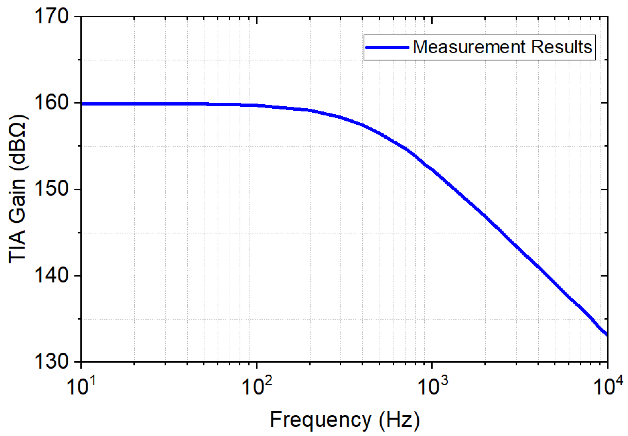
| TIA Gain (dBΩ) | 170 | 168 | 160 | 160 |
| Input-referred noise (pArms) | 0.4 | 4.2 | 1 | 1.8 |
Disclaimer/Publisher’s Note: The statements, opinions and data contained in all publications are solely those of the individual author(s) and contributor(s) and not of MDPI and/or the editor(s). MDPI and/or the editor(s) disclaim responsibility for any injury to people or property resulting from any ideas, methods, instructions or products referred to in the content. |
© 2023 by the authors. Licensee MDPI, Basel, Switzerland. This article is an open access article distributed under the terms and conditions of the Creative Commons Attribution (CC BY) license (https://creativecommons.org/licenses/by/4.0/).
Share and Cite
Kim, D.; Byun, S.; Pu, Y.; Huh, H.; Jung, Y.; Kim, S.; Lee, K.-Y. Design of a Current Sensing System with TIA Gain of 160 dBΩ and Input-Referred Noise of 1.8 pArms for Biosensor. Sensors 2023, 23, 3019. https://doi.org/10.3390/s23063019
Kim D, Byun S, Pu Y, Huh H, Jung Y, Kim S, Lee K-Y. Design of a Current Sensing System with TIA Gain of 160 dBΩ and Input-Referred Noise of 1.8 pArms for Biosensor. Sensors. 2023; 23(6):3019. https://doi.org/10.3390/s23063019
Chicago/Turabian StyleKim, Donggyu, Sungjun Byun, Younggun Pu, Hyungki Huh, Yeonjae Jung, Seokkee Kim, and Kang-Yoon Lee. 2023. "Design of a Current Sensing System with TIA Gain of 160 dBΩ and Input-Referred Noise of 1.8 pArms for Biosensor" Sensors 23, no. 6: 3019. https://doi.org/10.3390/s23063019