Article

3.6 mW Active-Electrode ECG/ETI Sensor System Using Wideband Low-Noise Instrumentation Amplifier and High Impedance Balanced Current Driver

Information and Communication System-on-Chip (SoC) Research Center, School of Electronics and Information, Kyung Hee University, Yongin 17104, Republic of Korea
*
Author to whom correspondence should be addressed.
Sensors 2023, 23(5), 2536; https://doi.org/10.3390/s23052536
Submission received: 26 January 2023 / Revised: 17 February 2023 / Accepted: 22 February 2023 / Published: 24 February 2023
(This article belongs to the Special Issue Advanced CMOS Integrated Circuit Design and Application II)

Abstract

:
An active electrode (AE) and back-end (BE) integrated system for enhanced electrocardiogram (ECG)/electrode-tissue impedance (ETI) measurement is proposed. The AE consists of a balanced current driver and a preamplifier. To increase the output impedance, the current driver uses a matched current source and sink, which operates under negative feedback. To increase the linear input range, a new source degeneration method is proposed. The preamplifier is realized using a capacitively-coupled instrumentation amplifier (CCIA) with a ripple-reduction loop (RRL). Compared to the traditional Miller compensation, active frequency feedback compensation (AFFC) achieves bandwidth extension using the reduced size of the compensation capacitor. The BE performs three types of signal sensing: ECG, band power (BP), and impedance (IMP) data. The BP channel is used to detect the Q-, R-, and S-wave (QRS) complex in the ECG signal. The IMP channel measures the resistance and reactance of the electrode-tissue. The integrated circuits for the ECG/ETI system are realized in the 180 nm CMOS process and occupy a 1.26 mm2 area. The measured results show that the current driver supplies a relatively high current (>600 μApp) and achieves a high output impedance (1 MΩ at 500 kHz). The ETI system can detect resistance and capacitance in the ranges of 10 mΩ–3 kΩ and 100 nF–100 μF, respectively. The ECG/ETI system consumes 3.6 mW using a single 1.8 V supply.

1. Introduction

Bioimpedance sensing has been an important research topic for investigating tissue properties, which provides valuable information for diagnosis, physiology, and pathology [1,2,3]. Dry electrodes have gradually replaced wet electrodes owing to the many advantages in personal healthcare and brain-computer interface applications [4,5]. Dry electrodes enable long-term monitoring in a user-friendly manner; however, they are exposed to relatively high variations in the electrode-tissue impedance [6]. This leads to interference in the wires that connect the electrodes to the readout circuit, thus reducing the signal quality. Some designs use analog buffers in the electrode [7]; this approach performs only impedance conversion, and it still places a stringent low-noise performance on the subsequent readout circuits. An alternative solution to this issue is using an active electrode (AE) containing a preamplifier [8]. This approach allows the electrodes to be placed close to the tissue. Noise interference is reduced by the short path from the electrode to the preamplifier, which relieves the noise requirement of the subsequent back-end (BE) circuits.
However, there are several challenges that are required to be addressed for this approach to be fully compatible with the electrocardiogram (ECG)/electrode-tissue impedance (ETI) sensing system [9,10]. The ETI system uses currents with different amplitudes and frequencies, which are injected into the tissue to measure the impedance spectrum. The variations in skin-electrode impedance are required to be resolved using a driver with a high output impedance over the bandwidth [11]. Various current drivers using the discrete designs of the balanced Howland topology have been reported [12,13]. This approach uses a pair of opamps and resistive networks in the feedback paths. The previous work [13] achieves an output impedance of 750 kΩ at 10 kHz, which is reduced to 330 kΩ at 300 kHz and eventually to 70 kΩ at 1 MHz. The maximum output current was approximately 1 mApp. However, the demand for very accurate matching of resistors makes the Howland topology incompatible with the integrated circuit (IC) design. Second, to obtain a high-quality signal, a preamplifier with a low-noise performance is required for AE. Moreover, electrode polarization, which can be up to a few hundred mV, may reduce the preamplifier headroom and saturate the output unless approaches handling the large DC offset are used. Another issue is that these requirements should be realized using low power to extend the battery life for portable applications.
To address the above challenges, in this work, we present a low-power AE-based integrated system for ECG/ETI measurement. To increase the output impedance, the current driver uses a matched current source and sink, operating under negative feedback. A new source degeneration method is proposed to increase the linear input range. The measured results show that the driver supplies a relatively high current (600 μApp) and achieves a high output impedance (1 MΩ at 500 kHz). To meet the stringent requirement of the AE, a preamplifier is designed using a capacitively-coupled instrumentation amplifier (CCIA) and active feedback frequency compensation (AFFC). The proposed CCIA achieves an excellent noise voltage density and 1/f noise corner of 65 nV/√Hz and 2.5 Hz, respectively. The back-end (BE) signal processing IC consists of five channels for three types of signal sensing, which are ECG, band power (BP), and impedance (IMP) data. The BP channel is successfully used to detect the Q-, R-, and S-wave (QRS) complex in the ECG signal. The IMP channel can measure the resistance and capacitance in the ranges of 10 mΩ–3 kΩ and 100 nF–100 μF. Characterization of the complete system shows successful detection of the motion artifact while measuring the ECG/ETI.
The paper is organized as follows. Section 2 describes the system architecture. Section 3 presents the design of the AE. Section 4 explains the design of the BE signal processing IC. Section 5 presents the measured results, and Section 6 draws the conclusion.

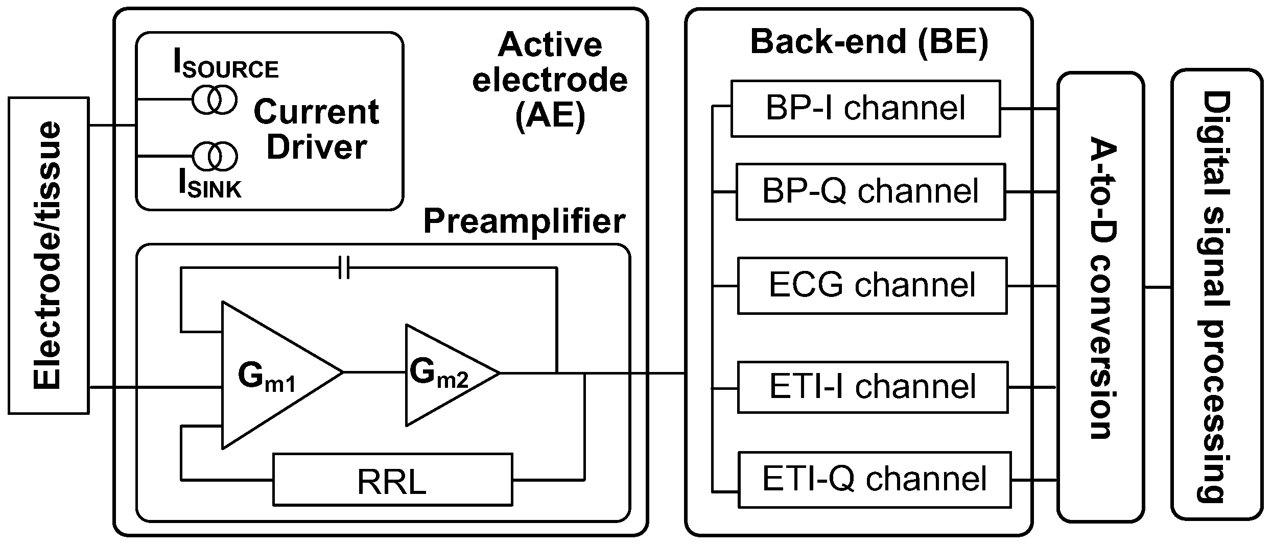
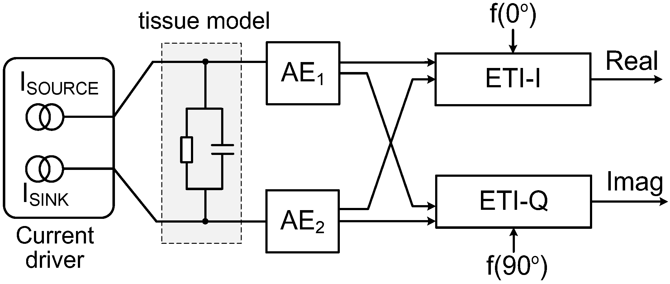
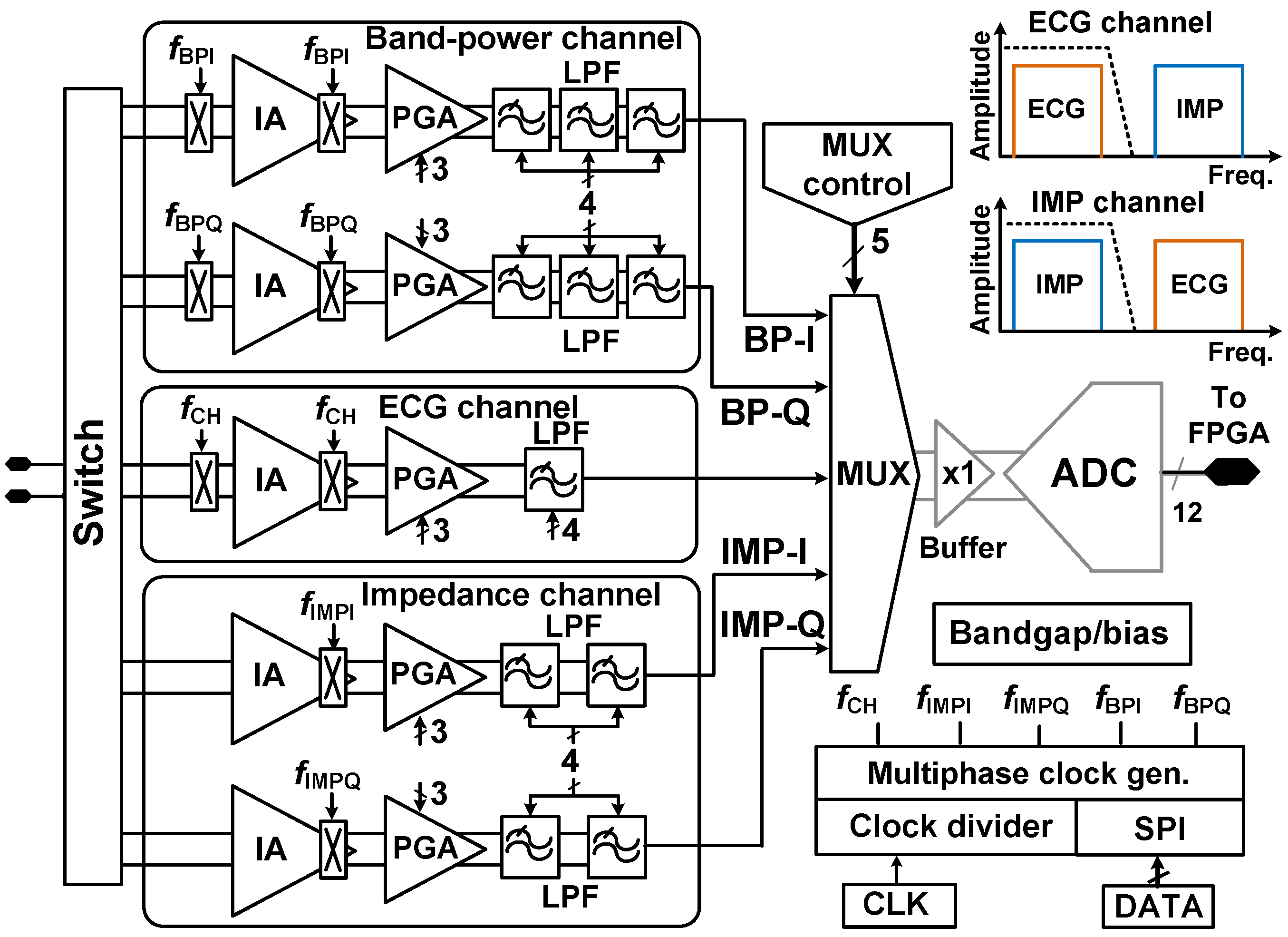
2. System Architecture

Figure 1 shows a block diagram of the proposed ECG/ETI system. The AE consists of a current driver and a preamplifier. The current driver includes matched current source and sink. The preamplifier, which is realized using CCIA, consists of two gain stages (Gm1, Gm2). The output ripple is suppressed using a ripple-reduction loop (RRL). The BE consists of five channels for three types of signal (ECG, BP, and IMP) sensing. To handle the in-phase and quadrature components, two sub-channels are used for BP and IMP measurement. The QRS complex in the ECG signal is detected using the BP channel. The IMP channel reads out the resistance and reactance, providing information on the electrode-tissue contact conditions. The ECG/ETI system is realized using a one-poly six-metal (1P6M) 180 nm CMOS process. The analog circuits are implemented using thick-oxide (3.3 V) transistors, which are tolerant up to 5 V. The digital circuits are realized using thin-oxide (1.8 V) transistors.
Figure 2 shows the schematic of the ETI measurement system. The current driver injects a balanced current into the tissue through the electrodes, which can be represented as i(t) = |I|cos(ωt), where the angular frequency is ω = 2πf. The corresponding voltages measured by the active electrodes (AE1 and AE2) can be written as v(t) = |V|cos(ωt + θ). Then, we can obtain the in-phase and quadrature components as
v ( t ) = | V | cos θ cos ( ω t ) | V | sin θ sin ( ω t ) = R ( t ) cos ( ω t ) X ( t ) sin ( ω t ) .
The signals are further processed using different phases to obtain resistance R(t) = |V|cos(θ)/|I| and reactance X(t) = |V|sin(θ)/|I|. Using the output of the in-phase and quadrature components, the spectral band power φ(f) of the BP channel can be expressed as
φ ( f ) = | R ( t ) w ( t ) [ cos ( 2 π f t ) ] d t | 2 + | X ( t ) w ( t ) [ sin ( 2 π f t ) ] d t | 2
where w(t) is the windowing function [14].

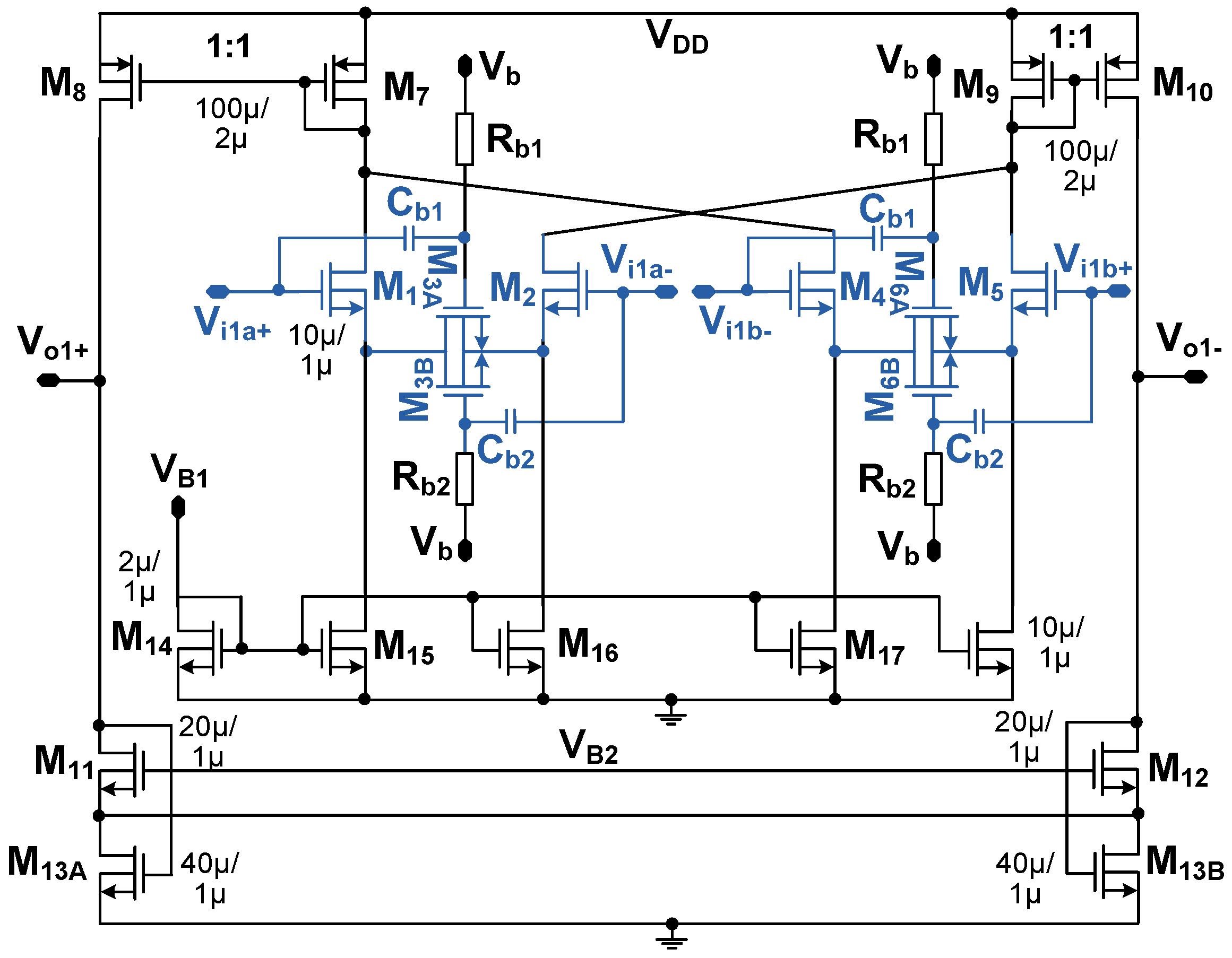
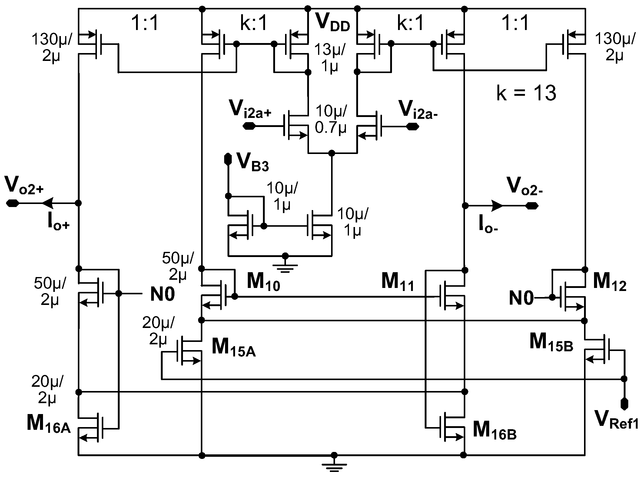
3. Active Electrode IC
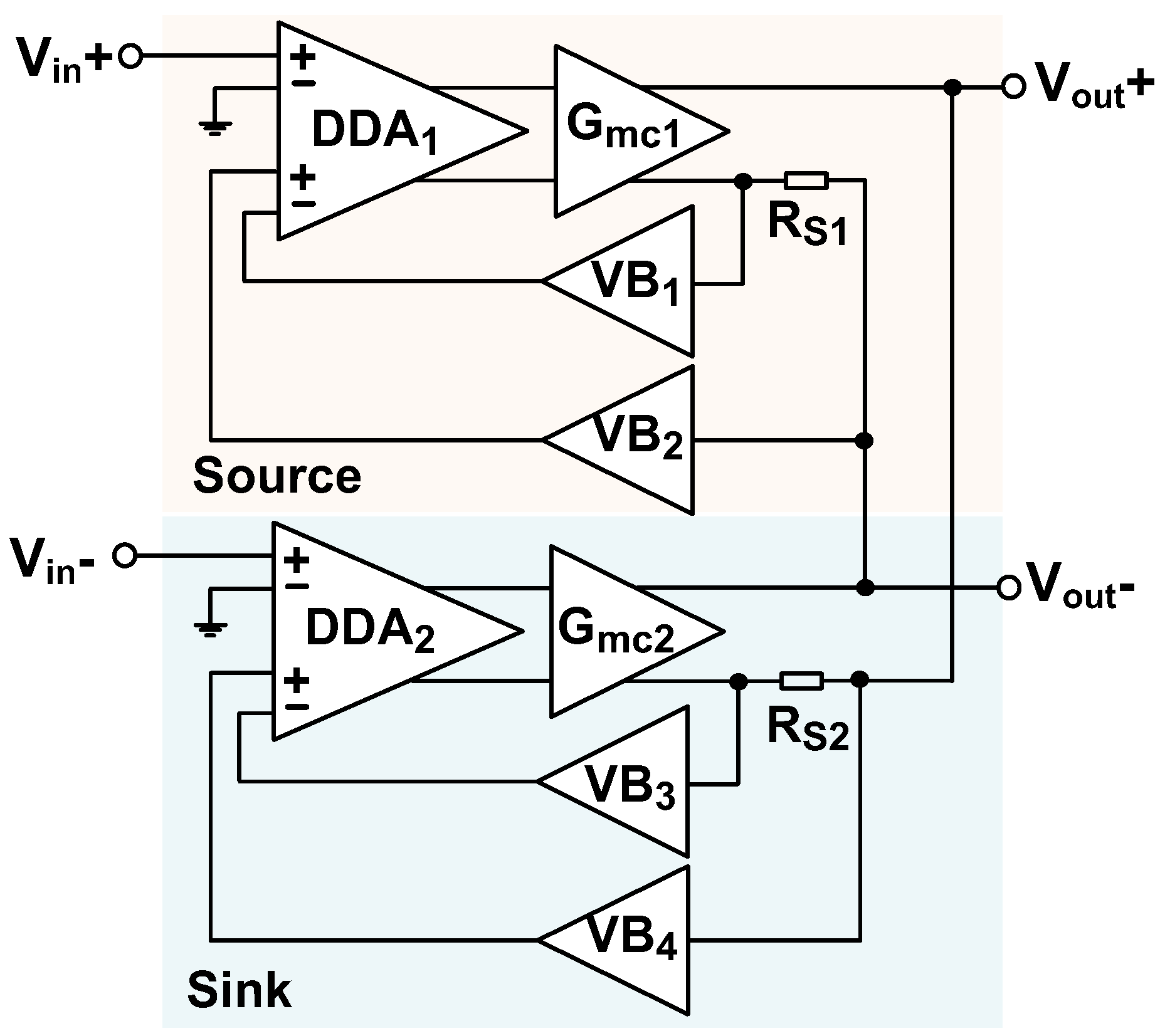
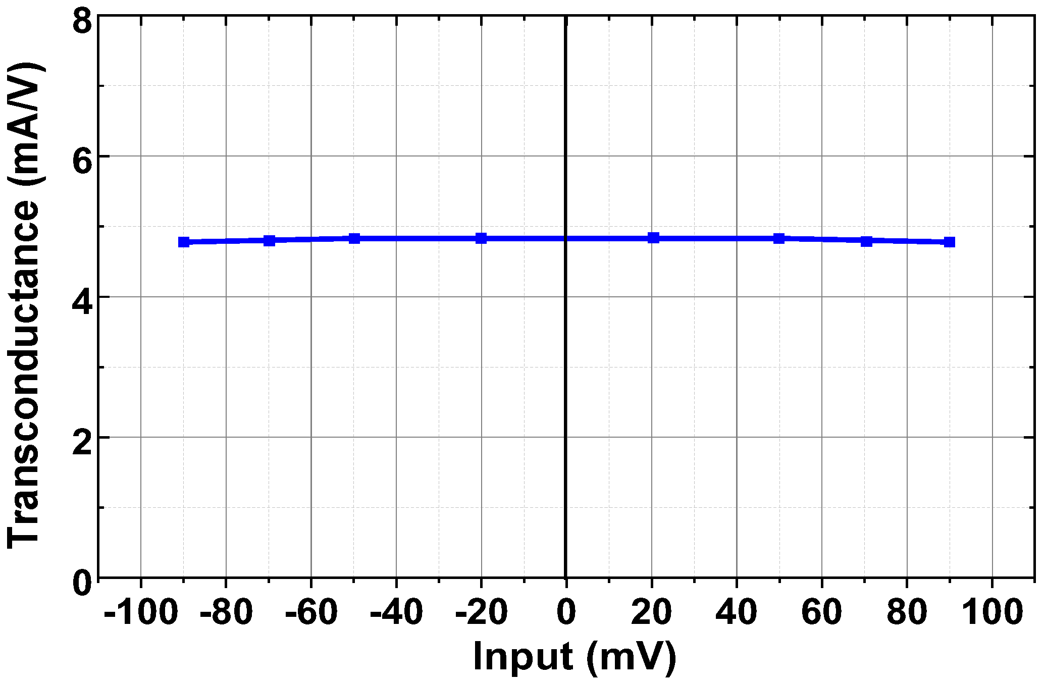
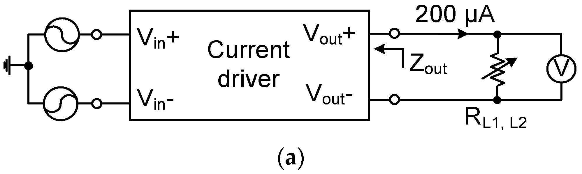
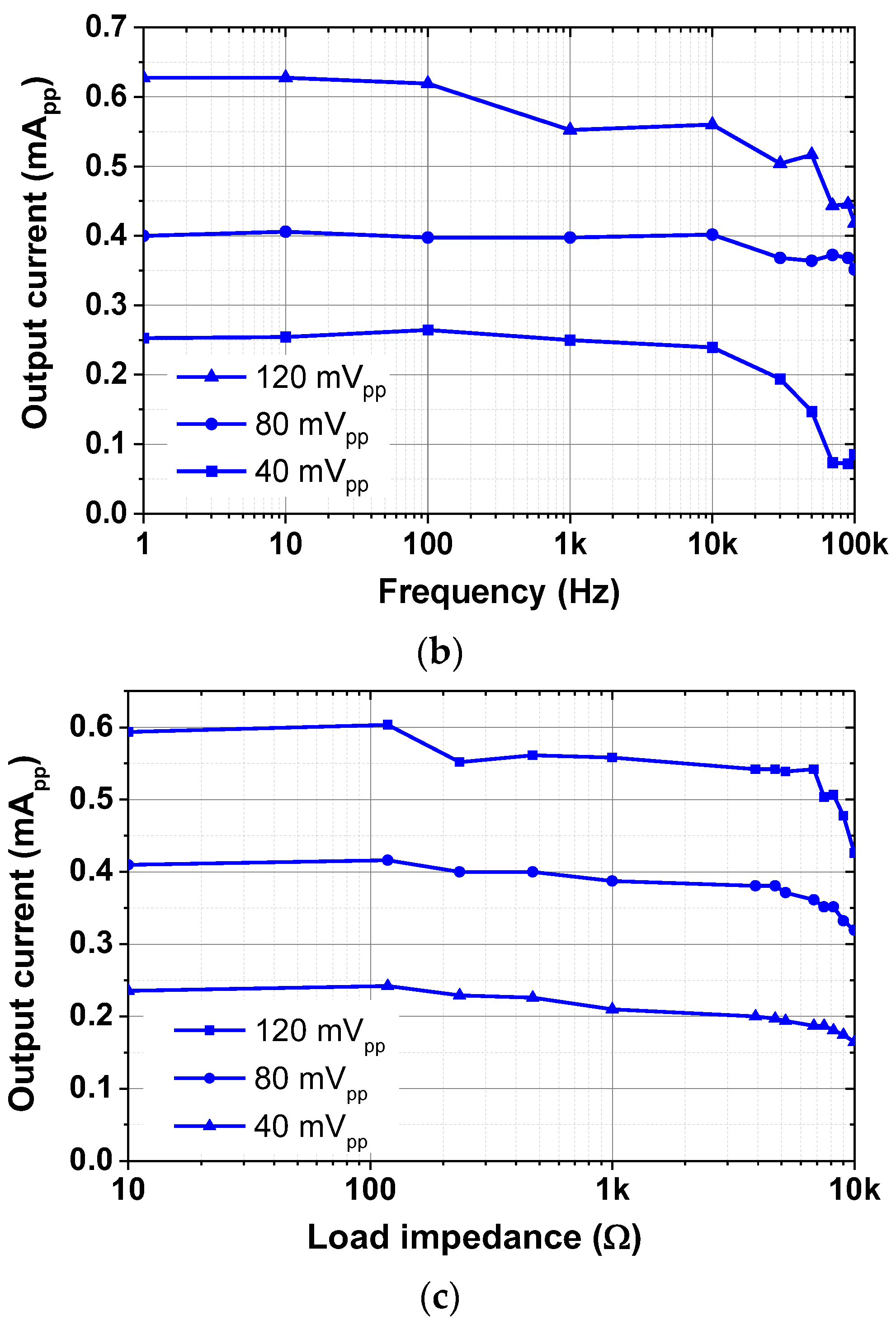
3.1. Current Driver

Figure 3 shows the schematic of the current driver. It consists of two identical sub-drivers to generate a balanced output. One is used for sinking current, and the other is used for sourcing current. This configuration can reject the common-mode (CM) voltage across the load caused by the mismatch in the transconductor (Gmc1,2) and sensing resistors (RS1,S2). Each sub-driver consists of a differential difference amplifier (DDA1,2) followed by the transconductor, which performs the voltage-to-current conversion. The RS1,S2 is used to monitor the output current, and the voltage across the resistor is fed back to the DDA1,2 through a pair of voltage buffers (VB1,2 and VB3,4), forming a negative-feedback loop. To accommodate a wide output swing, the buffers are designed to achieve a rail-to-rail output [11].
Source degeneration is used to extend the linear range. Figure 4a shows the previous approach of source degeneration [11], where the equivalent resistance of M3A,3B increases the input range. The current sources provide DC biasing to set the quiescent point on which the input AC signal is superimposed. M1 and M2 provide transconductance for the input voltage to current conversion. The current is converted to a voltage by the output resistance. The limitation of this approach is that it requires a relatively large input for M3A,3B to operate in the triode region.
Figure 4b shows the proposed approach where the control voltage of M3A,3B is provided by voltage Vb through a resistor Rb1,b2. This method allows the source degeneration to be controlled independently of the input level. Additionally, the gate of M3A,3B is connected to the input terminal through a small capacitor Cb1,b2, which allows tracking of the input variations. When the input (Vi1a+, Vi1a−) changes, Cb1,b2 senses the voltage and converts it to current. Then, the current charging the gate capacitance of M3A,3B creates the control voltage, which modulates the on-resistance for source degeneration. Figure 4c shows the comparison of the transfer characteristic obtained using the output and input signal amplitudes, which indicates the improved linearity of the proposed approach.
Figure 5 shows the schematic of DDA. M1,2 and M4,5 form the differential pair for the input transconductor. M3A,3B and M6A,6B provide source degeneration. The currents from the transconductors are summed at the drain of M7 and M9. M13A and M13B operating in the triode region provide the CM feedback control. The differential output voltage, (Vo1+Vo1−), can be written as
V o 1 + V o 1 g m 1 , 4 ( r o 8 | | r o 11 ) ( V i 1 a + + V i 1 b ) g m 2 , 5 ( r o 10 | | r o 12 ) ( V i 1 a + V i 1 b + ) = g m 1 ( r o 8 | | r o 11 ) [ ( V i 1 a + V i 1 a ) ( V i 1 b + V i 1 b ) ]
where gmi and roi represent the transconductance and output resistance of transistor Mi, respectively.
Figure 6 shows the schematic of the transconductor (Gmc1,2). It is implemented using the operational transconductance amplifier (OTA) with three current mirrors, which is similar to the one reported in [11]. In this work, the device sizing is modified to be compatible with the supply voltage VDD = 1.8 V. The circuit is fully symmetric, and a simple current mirror is used for reduced overdrive voltage. M16A and M16B, which operate in the triode mode, are used to set the DC bias. We use VRef1 in the secondary current mirror so that M15A and M15B working in the triode region provide additional means of stabilizing the output DC level.

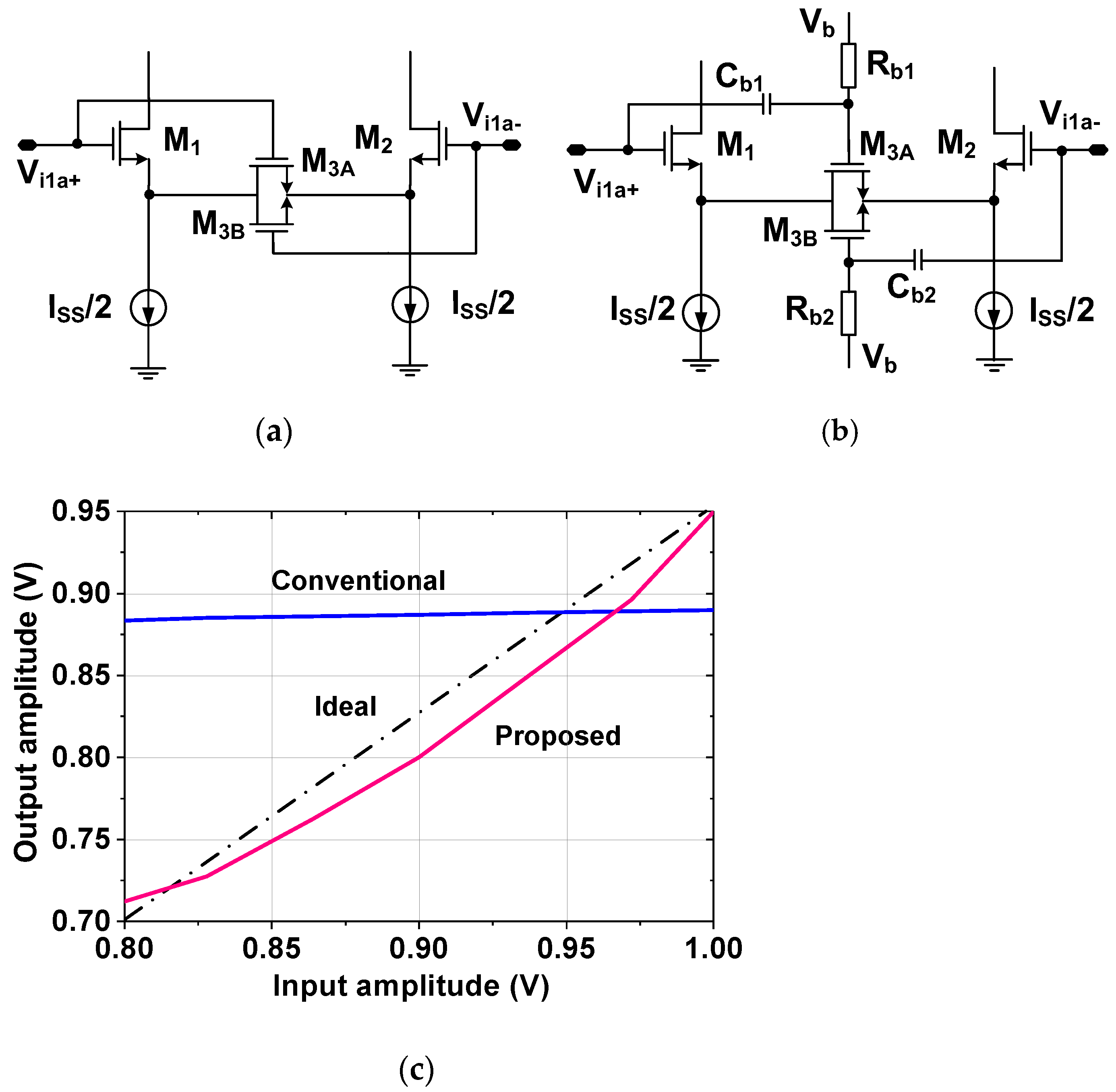
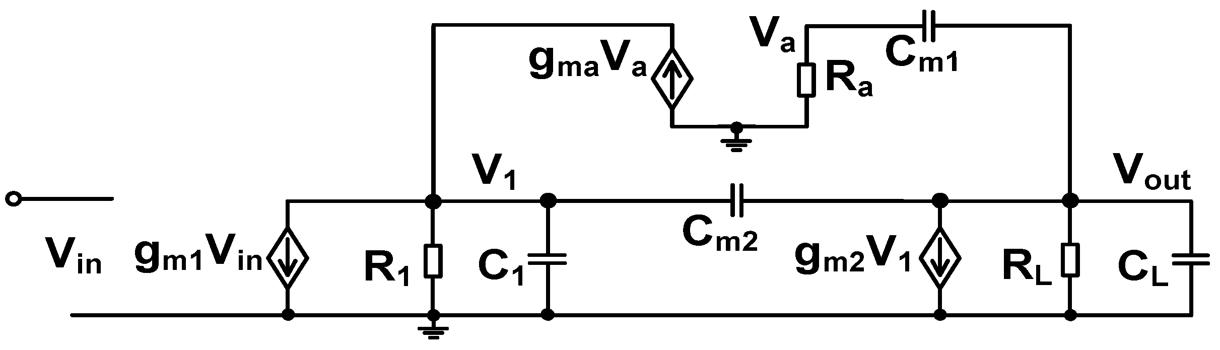
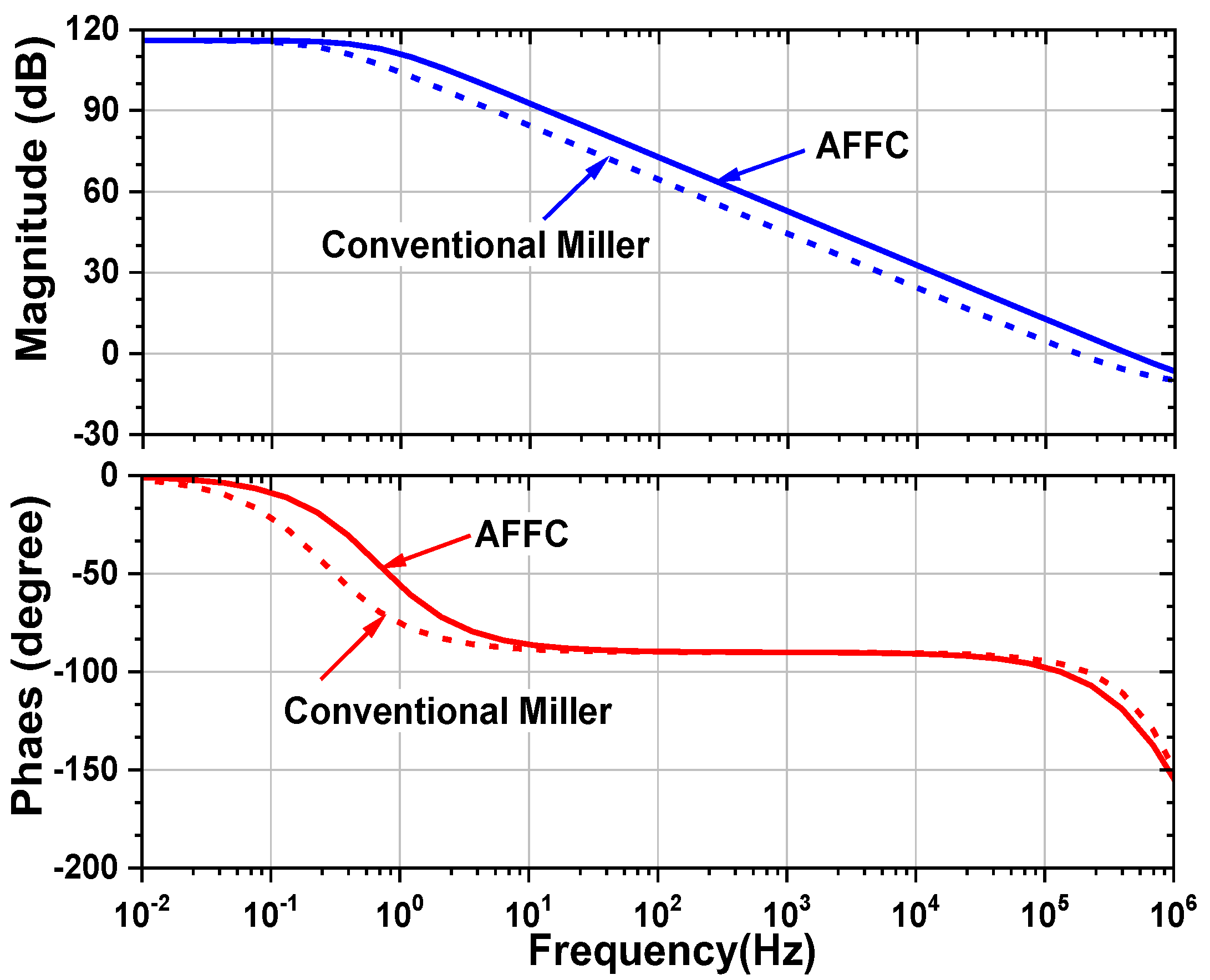
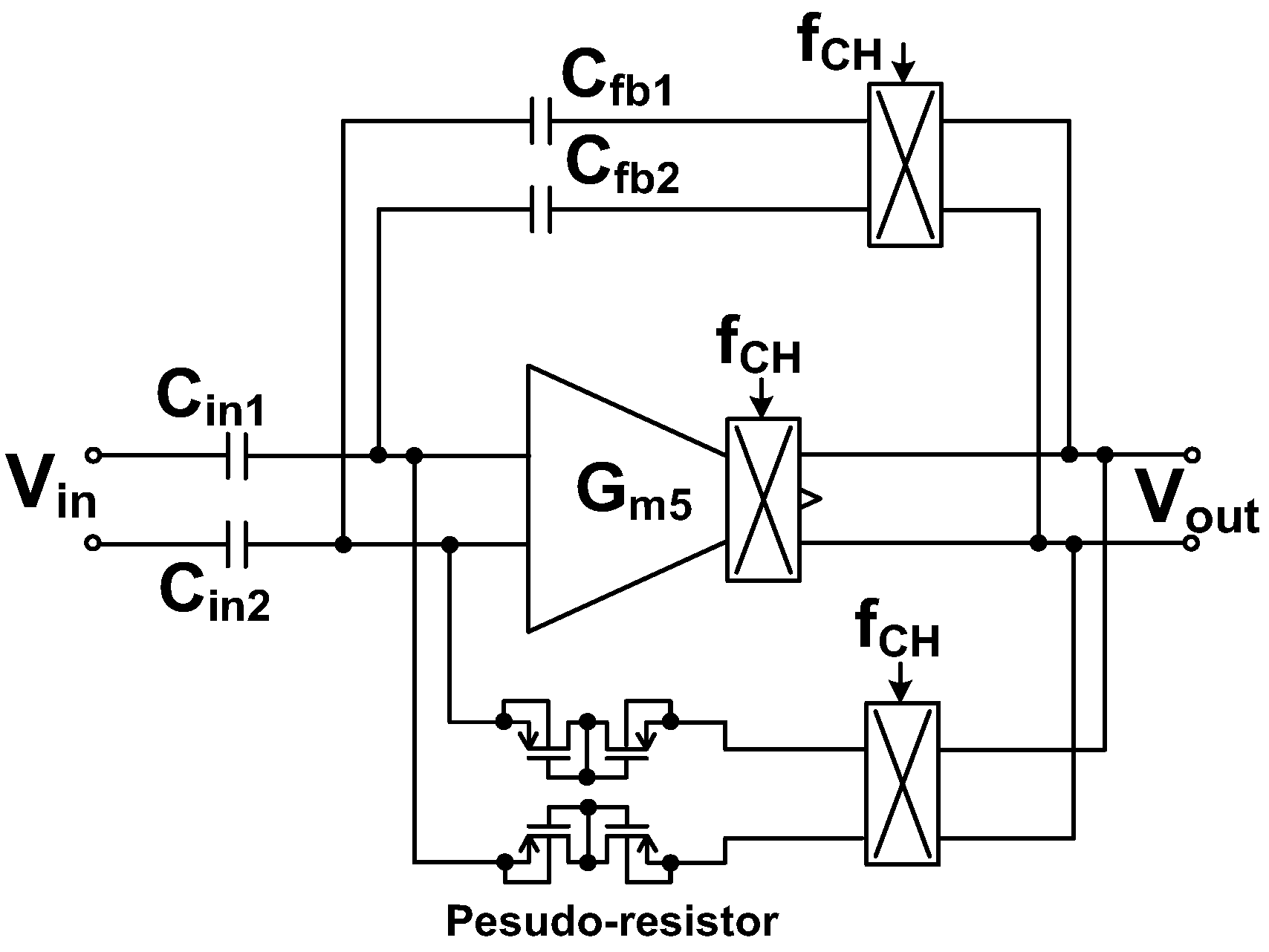
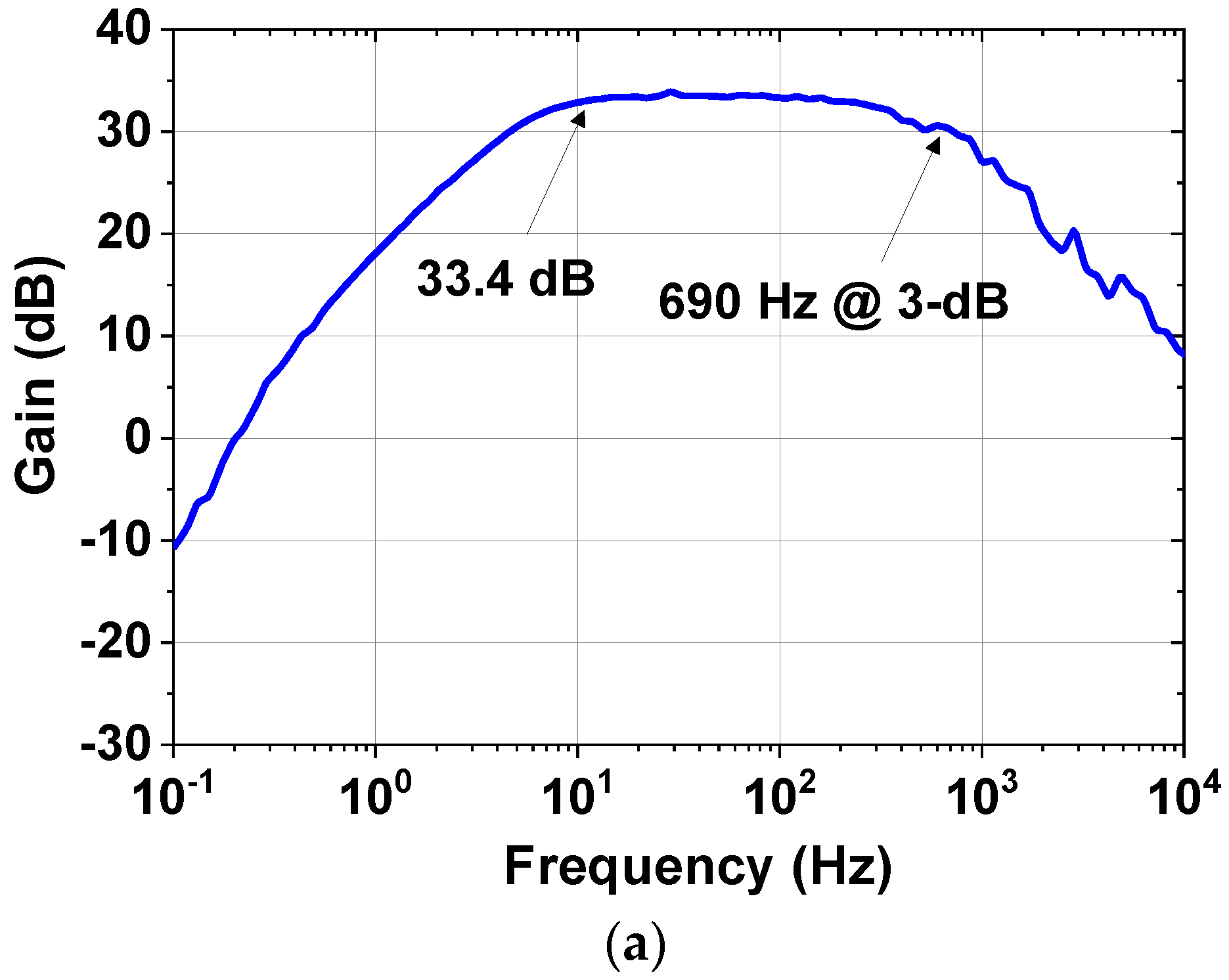
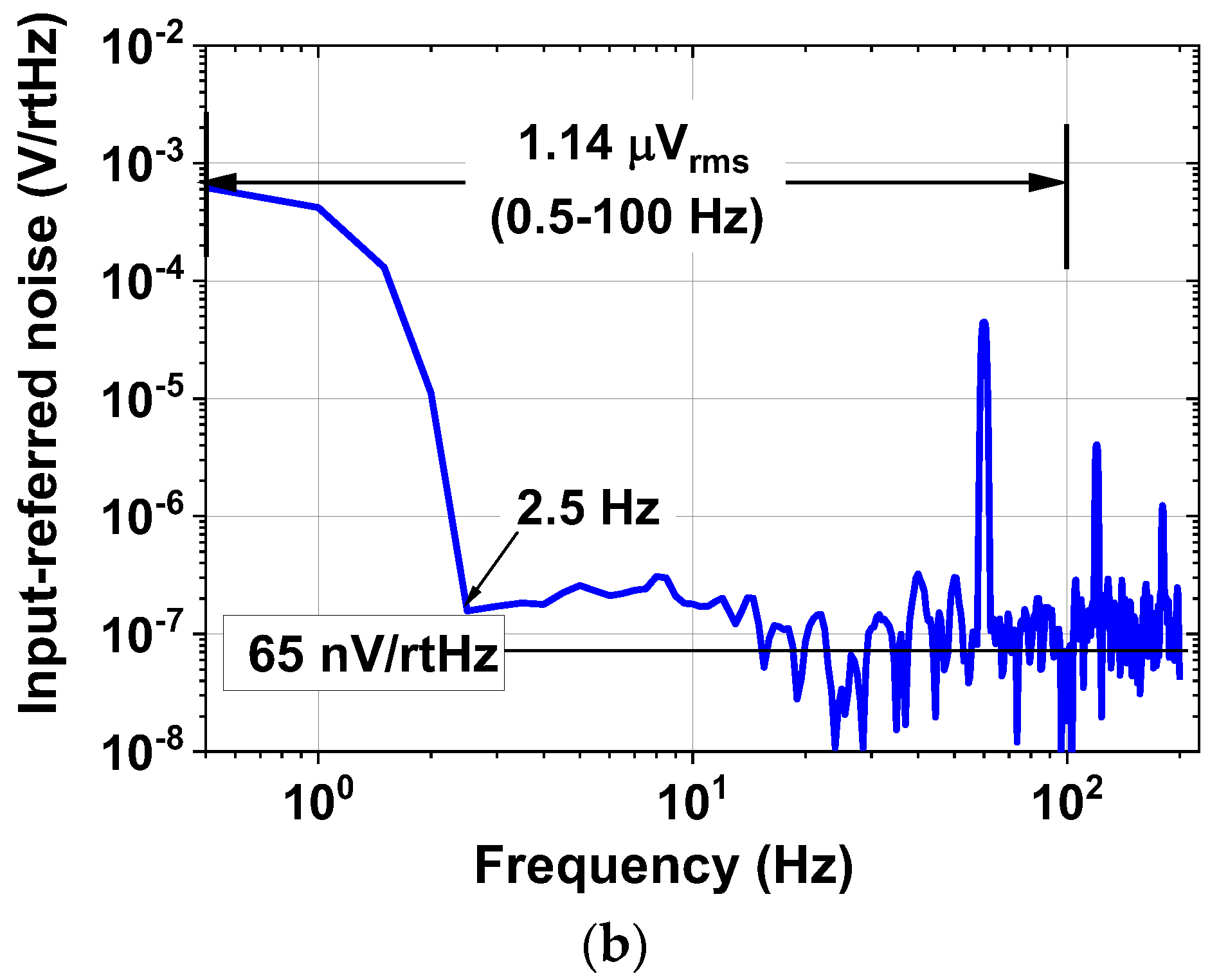
3.2. Instrumentation Amplifier

Figure 7 shows the schematic of the preamplifier. It consists of two gain stages. The first stage (Gm1) is realized using a folded-cascode differential amplifier [15]. The second stage (Gm2) is implemented using a common-source amplifier to increase the output swing. Feedback loops are used to set the mid-band gain through Cfb1,2 and the bias of the input node through pseudo-resistors. To suppress the output ripple, the RRL forms another feedback loop. For the RRL, continuous-time implementation is used because the discrete-time approach based on sampling increases the in-band noise through noise folding [16].
The input signal is upconverted by the chopper CH1, operating at the chopping frequency fCH. The signal is amplified by Gm1, and the output is downconverted by the chopper CH2. The offset at the input of Gm1 is upconverted and filtered out by the low-pass characteristic of the amplifier. A capacitive coupling consisting of the input (Cin1,2) and feedback capacitors (Cfb1,2) is built around the two-stage opamp (Gm1 and Gm2). The combination of CH1 and Cin1,2 creates an equivalent input resistance of (1/2fCHCin1,2). Similarly, CH3 and Cfb1,2 create an equivalent resistance of (1/2fCHCfb1,2). The two resistances form a feedback loop around the opamp.
Nested Miller compensation has been used to achieve stability under a wide range of capacitive loads [15]; however, for stability, the size of the compensation capacitor should be increased in proportion to the load capacitance. Moreover, this approach suffers from bandwidth reduction. In this work, we use AFFC, which has the advantage of extending the bandwidth using a small compensation capacitor. The AFFC is implemented using a cascode Miller (gma and Cm1) in parallel with a Miller capacitor (Cm2) [17]. The cascode Miller, which is implemented using a common-gate transconductor, blocks the feedforward signal that exists in the traditional Miller compensation. Compared to the passive compensation, the gain provided by gma reduces the size of Cm1. Cm2 is used to control the Q-factor for stability. The noise power contribution of the AFFC to the input-referred noise is relatively small when divided by (AV1)2, where AV1 ≈ 60 dB is the voltage gain of the first stage.
Figure 8 shows the schematic of the folded-cascode differential amplifier (Gm1). Two additional sets of choppers are embedded in the amplifier. One chopper is placed at the output of the cascode transistors to demodulate the signal down to the baseband while modulating the input offsets to the fCH band. Another one is placed at the drain of the current source to upmodulate the flicker noise. At the output of the amplifier, the signal returns to the baseband while the offset and flicker noise is modulated to high frequency, which is filtered by the second stage. The common-mode feedback (CMFB) loop is realized using the two differential pairs. The CMFB loop may have poles of higher frequency than that of the differential-mode (DM) loop. Therefore, we design the CMFB loop to have a smaller unity-gain frequency than the DM loop. Considering the frequency response, we determine the sizing of the two differential pairs.
Figure 9 shows the equivalent small-signal model of the amplifier. Because the open-loop gain is calculated, we obtain the model by removing the feedback loops in Figure 7. It includes transconductances (gm1, gm2, and gma) and Miller capacitors (Cm1, Cm2). R1 and C1 are the output resistance and capacitance of the first gain stage, respectively. R1 is determined by the output resistance of the cascode stage, and C1 is the sum of capacitance at the output. The RL and CL are the load resistor and capacitor, respectively.
Using the circuit model, the open-loop gain of the amplifier can be expressed as.
A V ( s ) A DC ( 1 + s C m 1 / g m a ) g m a ( 1 s C m 2 / g m 2 ) s 3 R 1 R L C m 1 C m 2 C L + s 2 R 1 R L C m 2 ( g m a C L + g m 2 C m 1 ) + s R 1 R L g m 2 g m a ( C m 1 + C m 2 ) + g m a
where ADC = (gm1gm2R1RL) is the low-frequency gain. AFFC creates a left-hand plane (LHP) zero, extending the amplifier bandwidth. Assuming the conditions of (CL, Cm1, and Cm2) >> C1, (gm1R1, gm2RL) >> 1, and (gmaCL) >> (gm2Cm1), we obtain two zeros (z0 and z1) and three poles (p0, p1, and p2) as
z 0 = z LHP = g m a C m 1   z 1 = z RHP = g m 2 C m 2 , p 0 1 R 1 R L g m 2 ( C m 1 + C m 2 ) ,   p 1 g m 2 ( C m 1 + C m 2 ) C m 2 C L ,   p 2 g m a C m 1 .
The 3-dB frequency is determined by p0, resulting in the gain-bandwidth product of GBW = gm1/(Cm1 + Cm2). The right half plane (RHP) zero introduces the phase lag (−tan−1(GBW/zRHP)) similar to the pole (−tan−1(GBW/p0,1,2)), which reduces the phase margin (PM). The extra phase shift caused by the RHP zero degrades the amplifier stability, and the Miller capacitor (Cm2) is used for frequency compensation.
To realize a maximally flat frequency response for stability, the Q-factor can be set to 0.7 [18]. Owing to the positive phase shift provided by LHP zero (zLHP), AFFC can extend the bandwidth of the single-stage amplifier by more than two times [19]. Therefore, when p1 is placed close to twice the value of GBW, the amplifier stability can still be achieved as
| p 1 | 2 GBW = 2 g m 1 ( C m 1 + C m 2 ) .
To compensate for the negative phase shift caused by p1, the location of z0 is selected as
| z 0 | = g m a C m 1 = 2 | p 1 |
Using Equations (6) and (7), we obtain the expression for gma as
g m a = 2 2 g m 1 C m 1 C m 1 + C m 2
To obtain the expression for Cm1, we substitute p1 of Equation (5) into Equation (7). Using the expression for gma given by Equation (8), we obtain
C m 1 = 2 g m 1 C m 2 C L g m 2 C m 2
where we use relatively small capacitors of Cm1 = 0.8 pF and Cm2 = 0.2 pF. The gma is implemented using a common-gate transistor having a size of (W/L) = 0.9 μm/0.7 μm. The PM of the amplifier with pole-zero cancellation can be expressed as
PM = 90 ° tan 1 [ GBW / p 1 , 2 Q ( 1 ( GBW / p 1 , 2 ) 2 ) ] + tan 1 ( GBW z 0 )
where the quality factor is expressed as Q = |p1,2|/(2|Re{p1,2}|) in case when complex poles are formed for p1 and p2 [20]. A detailed derivation of the complex poles and the Q-factor can be found in the Appendix A.
Figure 10 shows the comparison of the open-loop gain of the amplifier using AFFC and conventional Miller compensation. The bandwidth is extended by the LHP zero available in the AFFC. The PM is reduced from 82.2° to 60°; it guarantees stable operation. Figure 11 explains the operation of the RRL, and its implementation is similar to the previous work [21]. The process variation creates offsets. Gm1 and Gm2 are associated with the offset voltages VOS1 and VOS2, respectively. The VOS2 is not chopped but suppressed by the open-loop gain (AOL1) of the preceding stage (Gm1). Therefore, the input-referred offset can be written as (VOS1 + VOS2/AOL1). The system offset amplified by Gm1 creates the offset current. The current is up-converted to fCH by CH2, and integrated by Gm2 and Cm2, producing the output ripple Vout,ripple. At the output, a sense capacitor CS1 converts Vout,ripple to a current IAC,ripple. The current demodulated by the chopper CH3 is converted to IDC,ripple. The current integrated by Gm3 and Cint generates the integrator output Vint, which is converted to the voltage VRRL by Gm4. To cancel the offset current generated by VOS, the VRRL is input to Gm1.

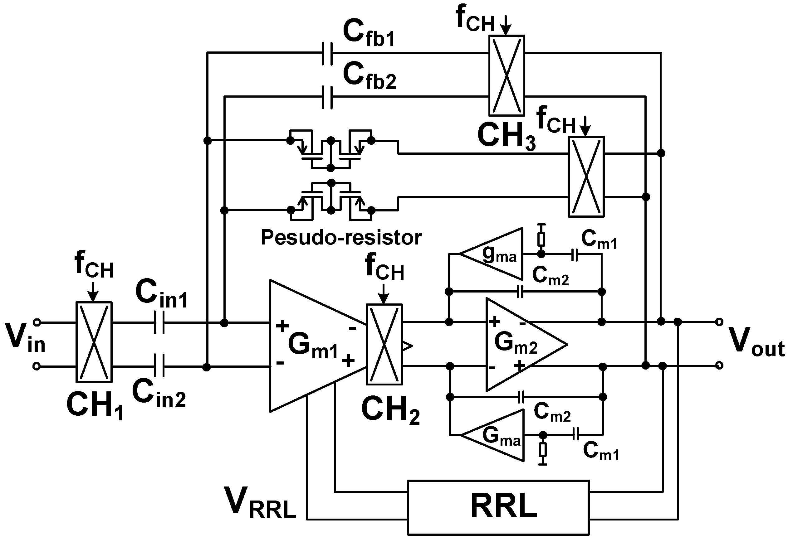
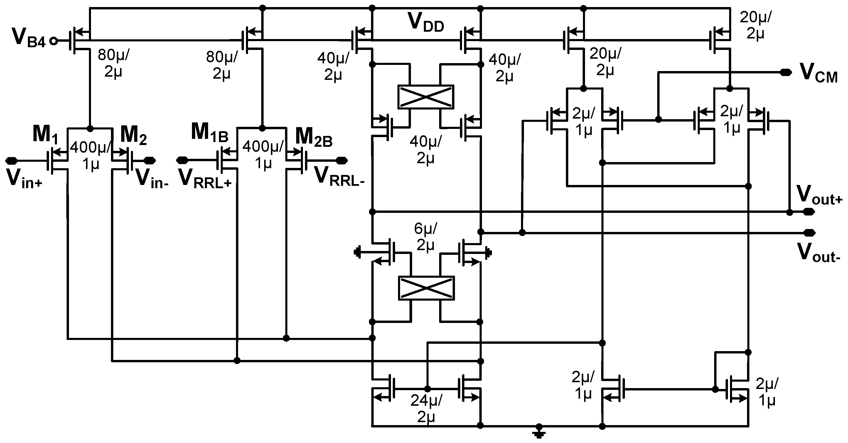
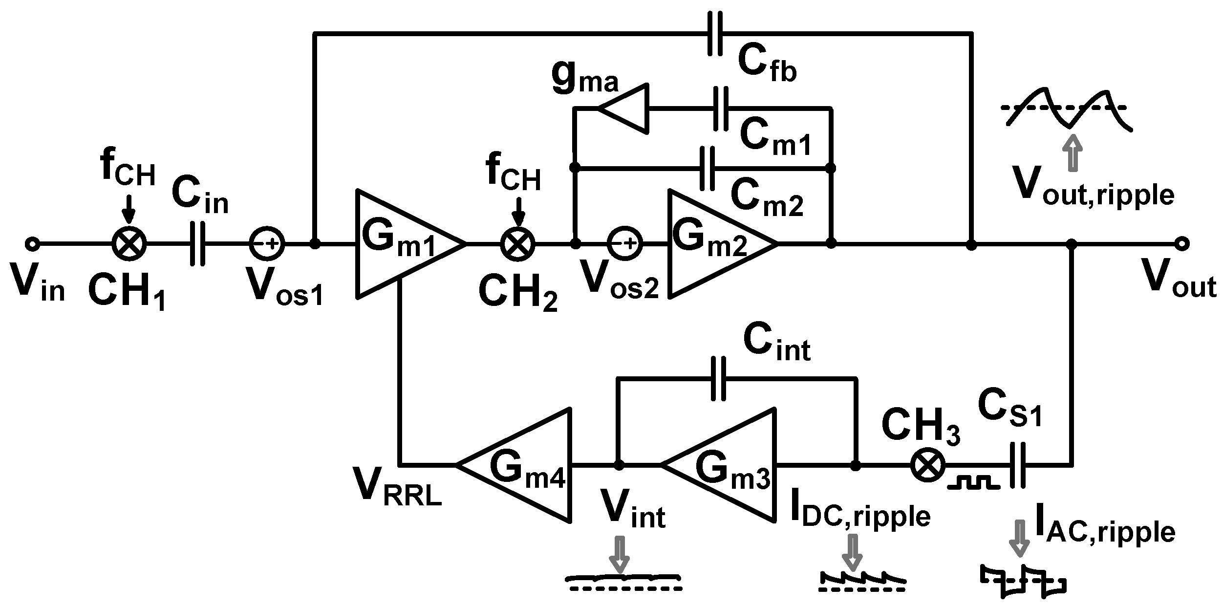
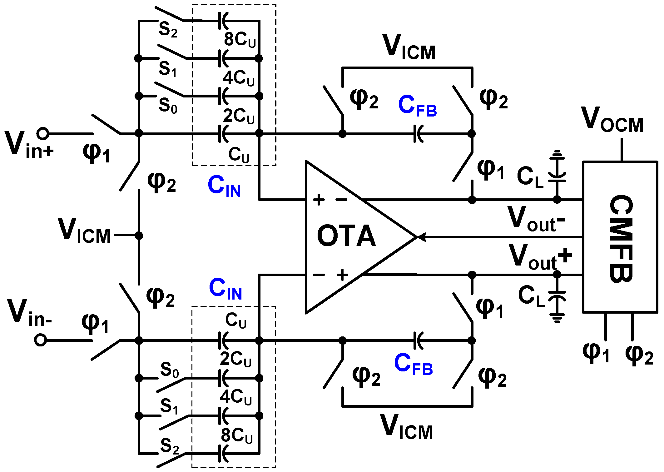
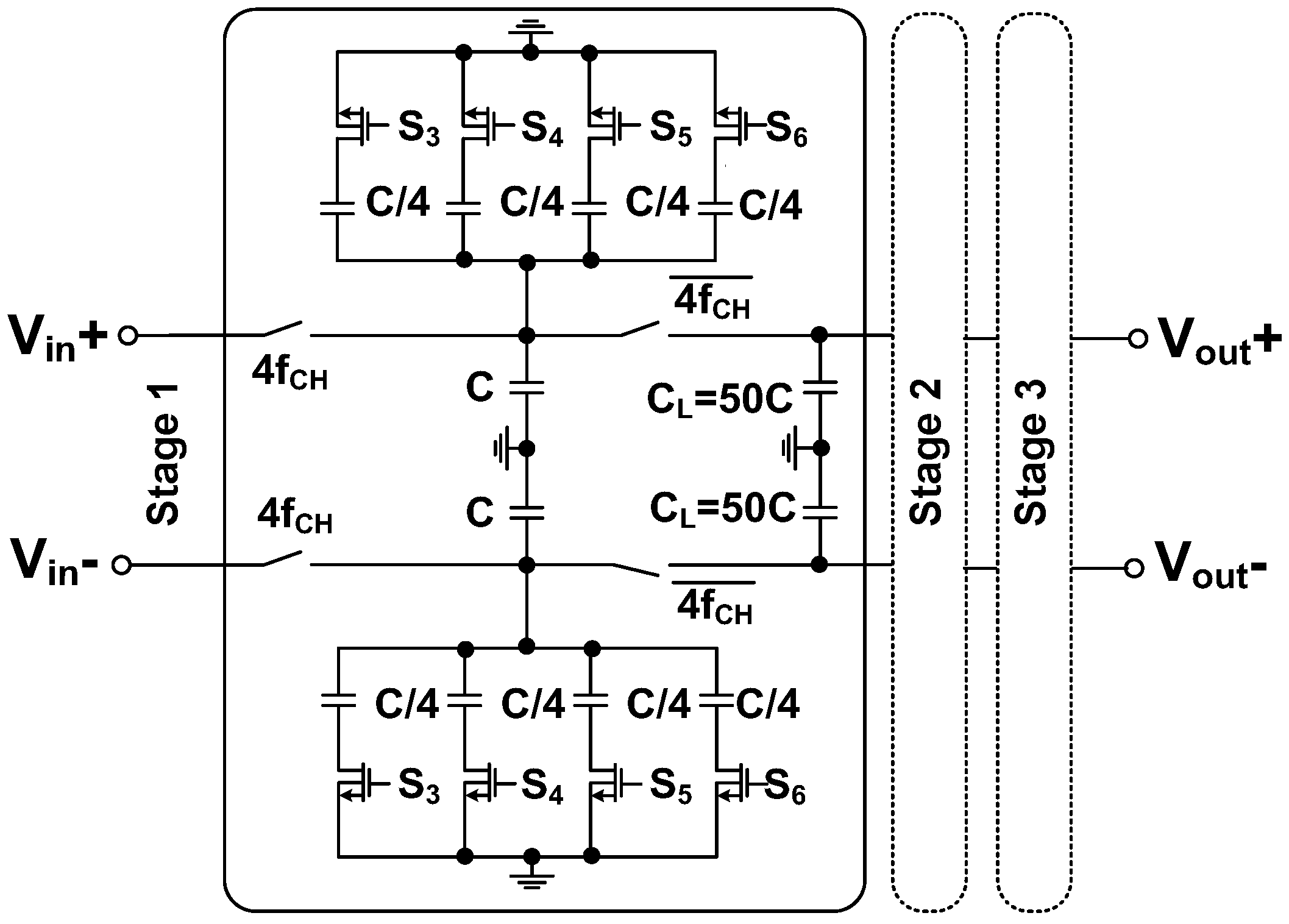
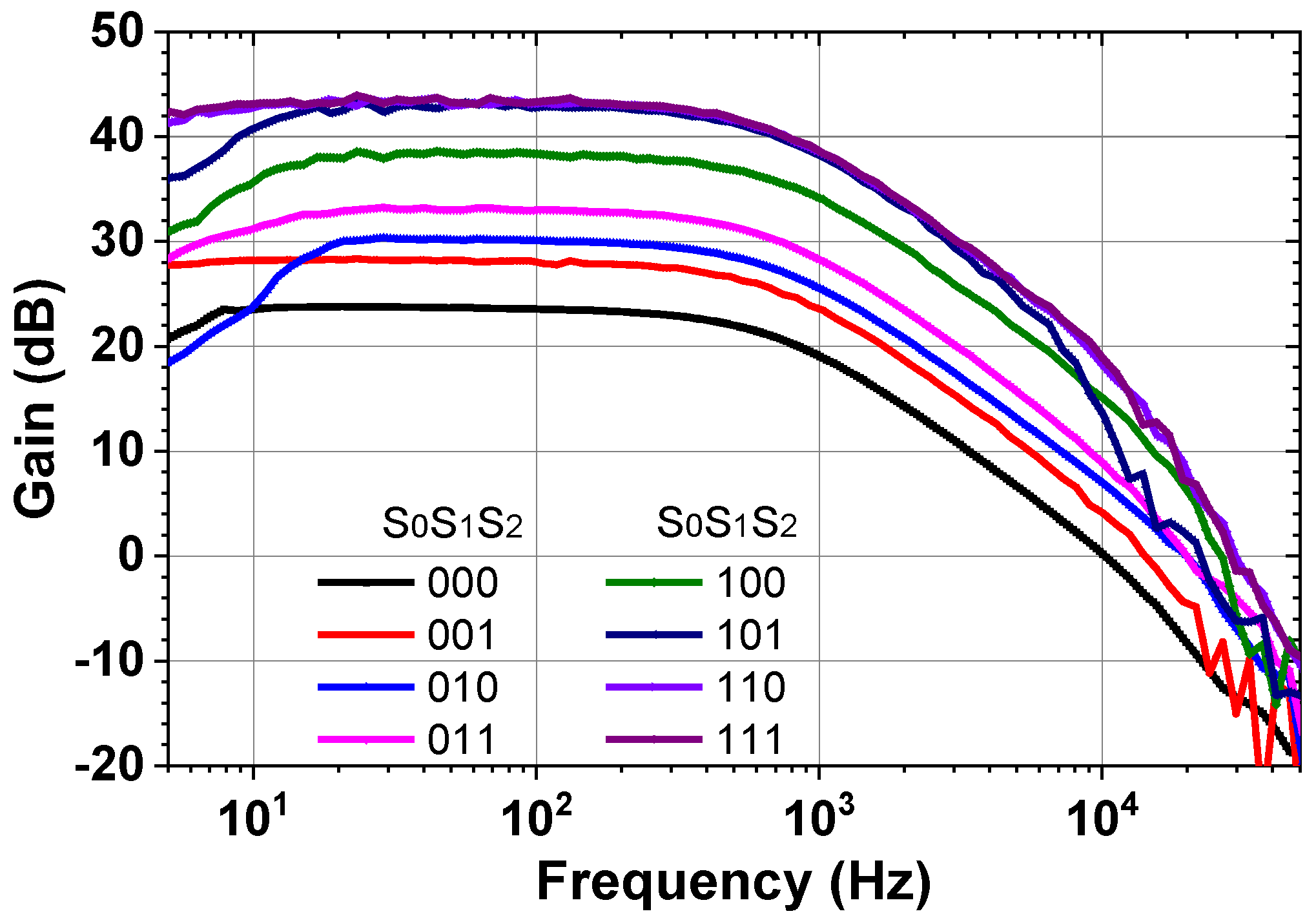
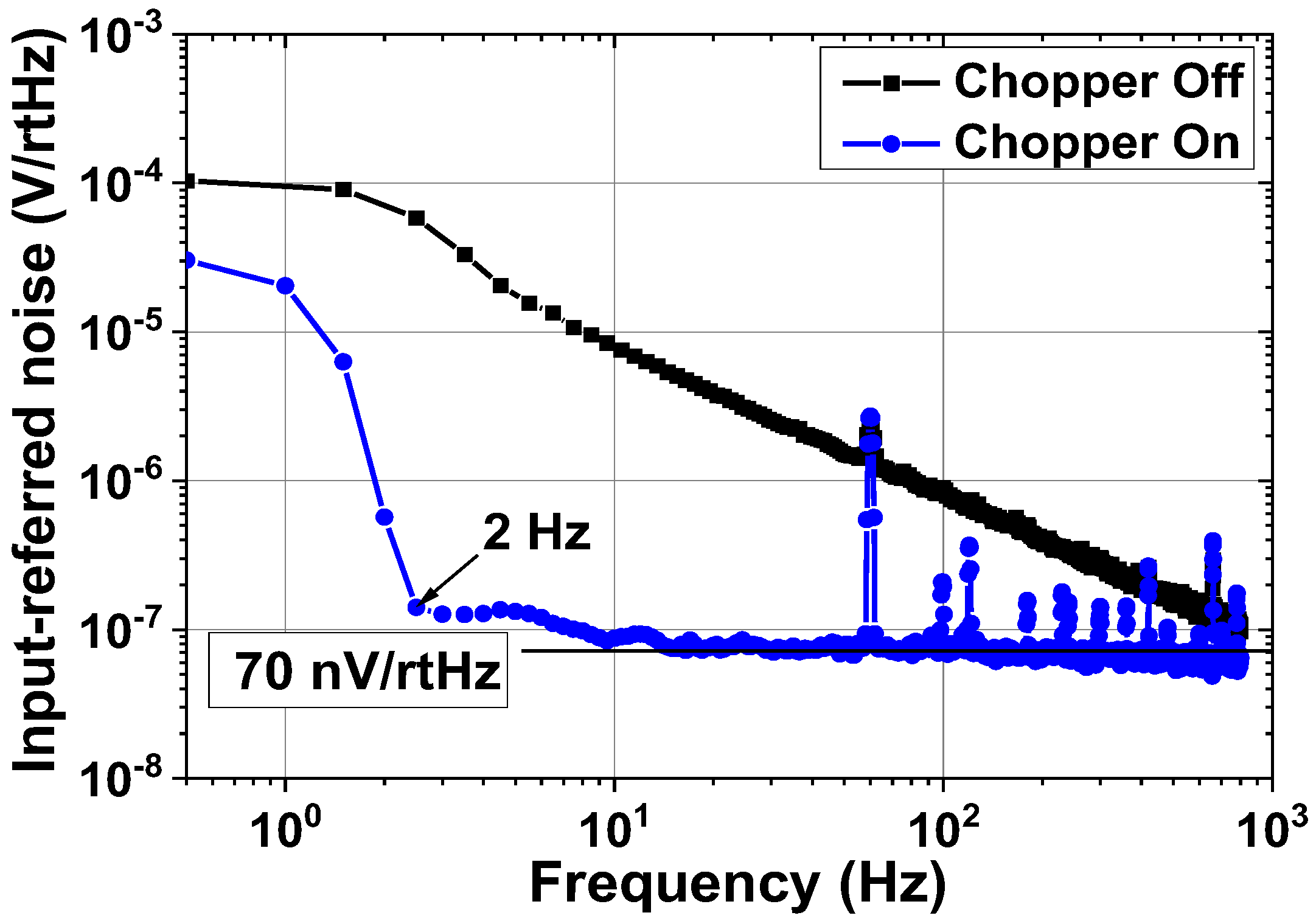
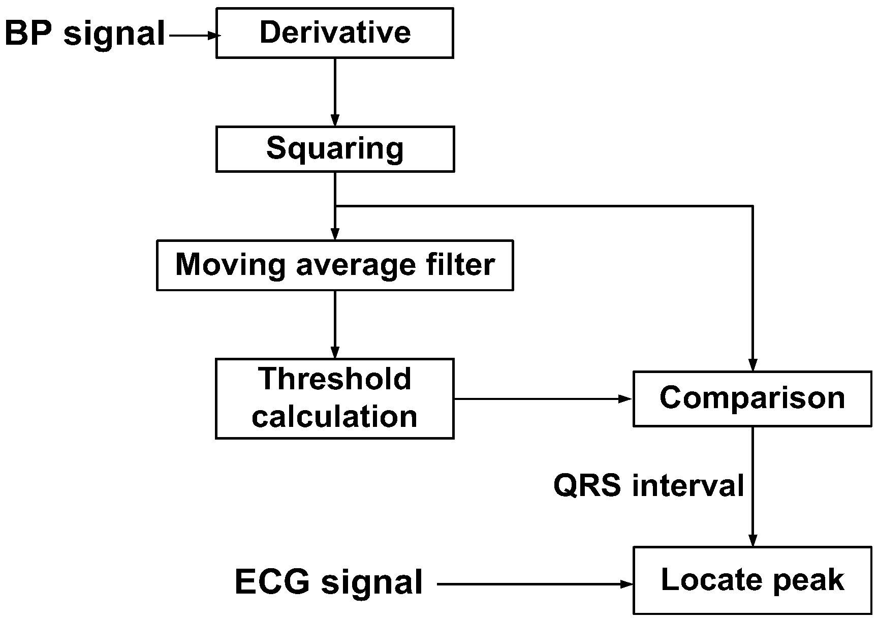
4. Back-End Signal Processing IC
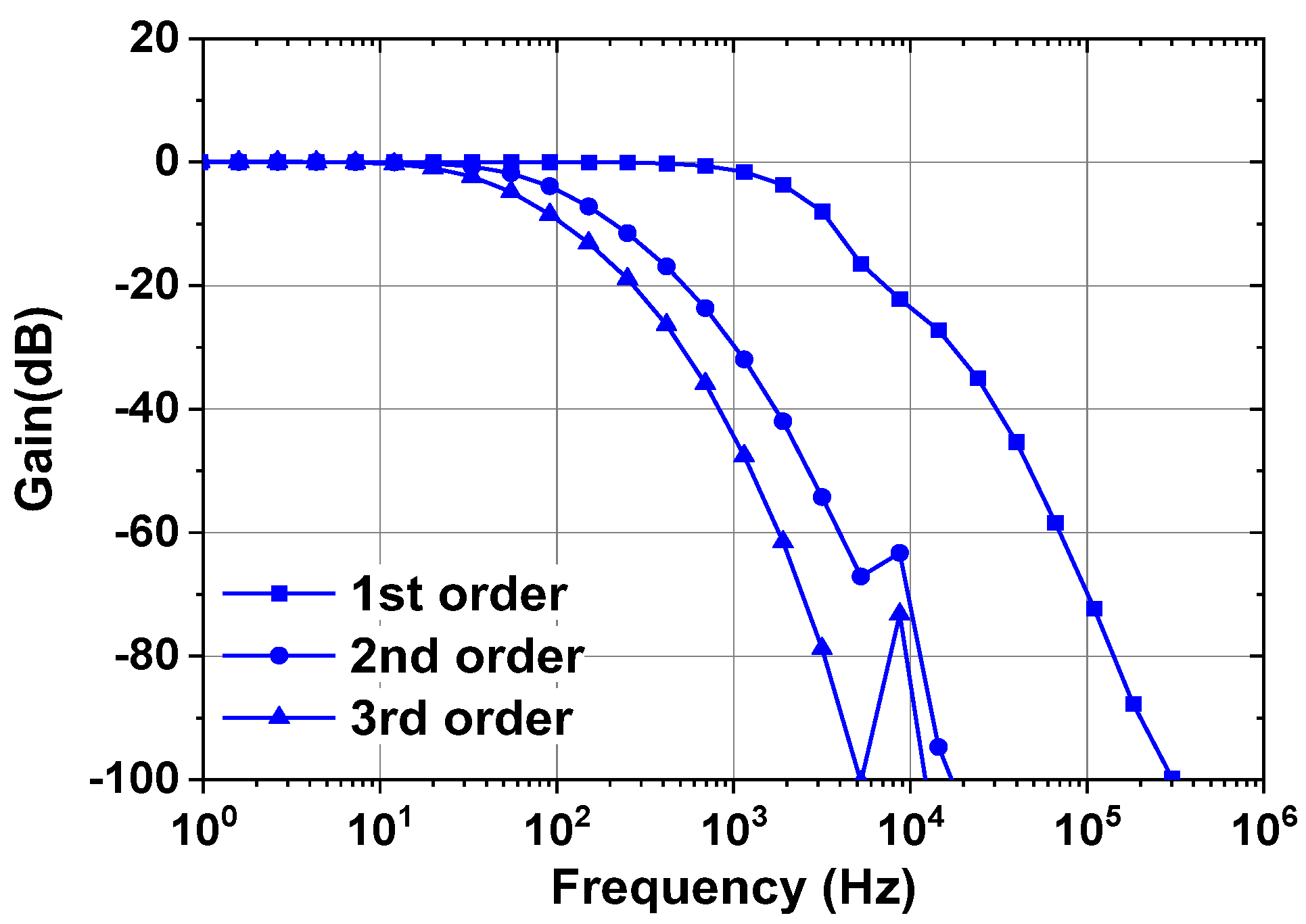
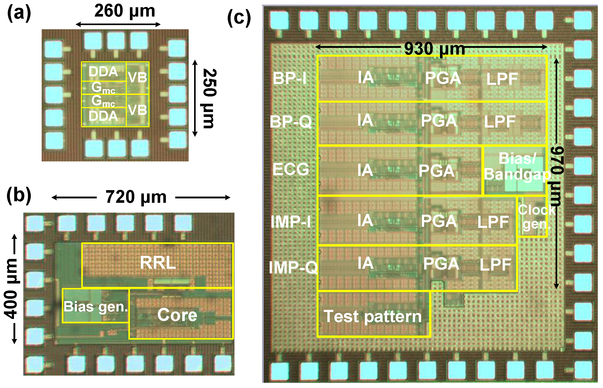
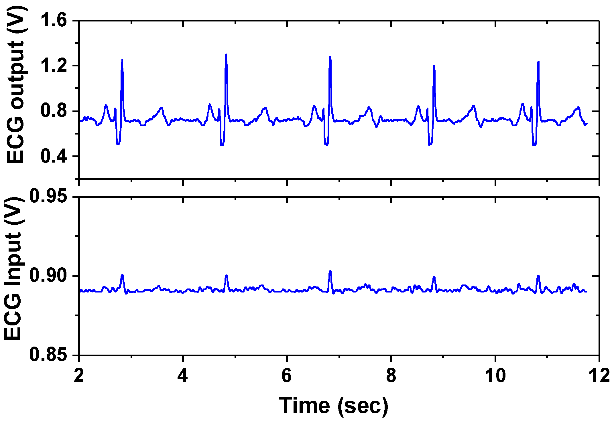
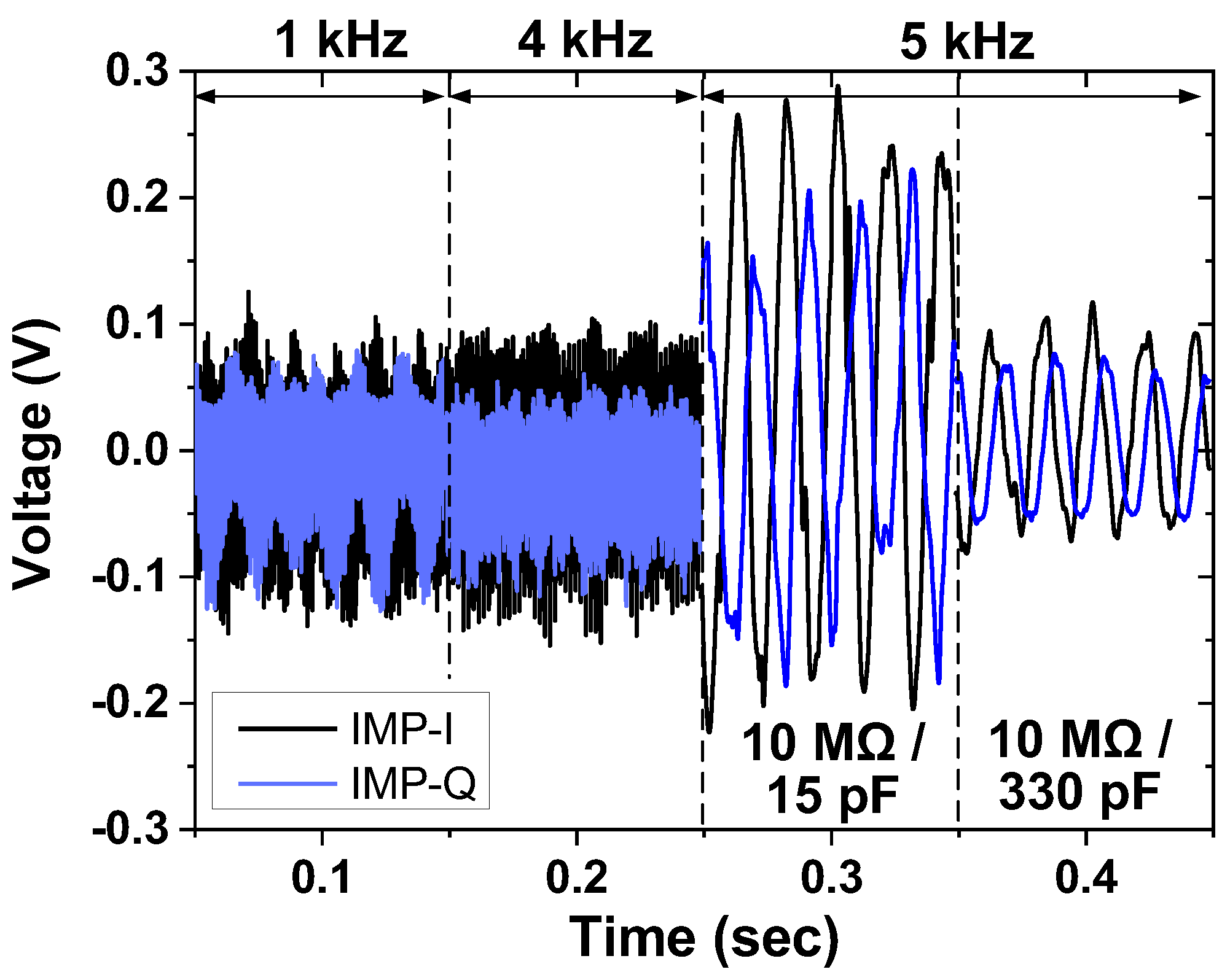
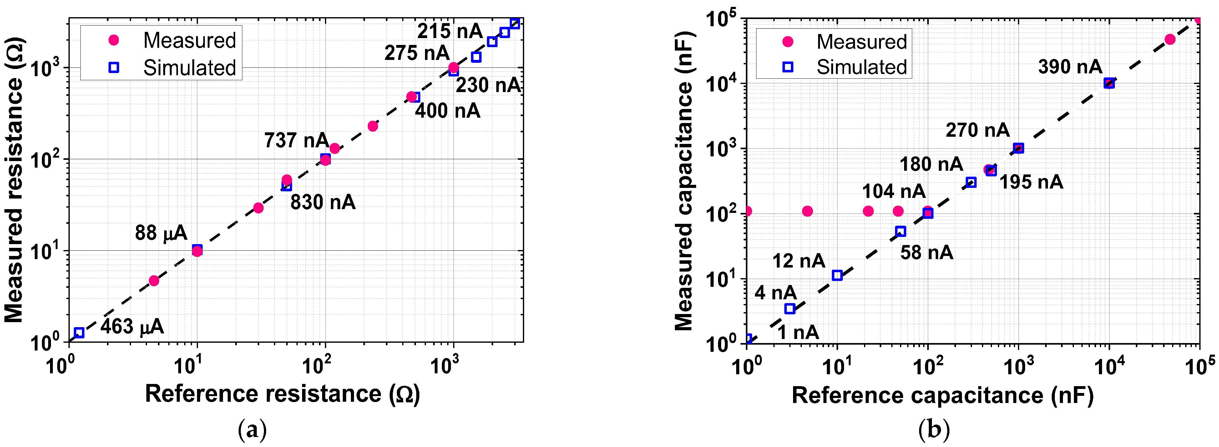
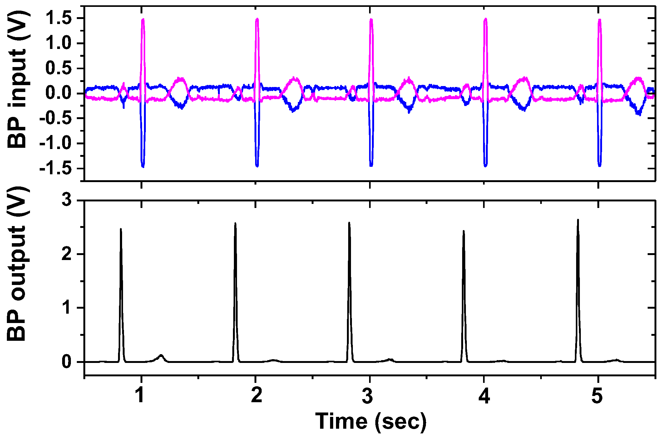
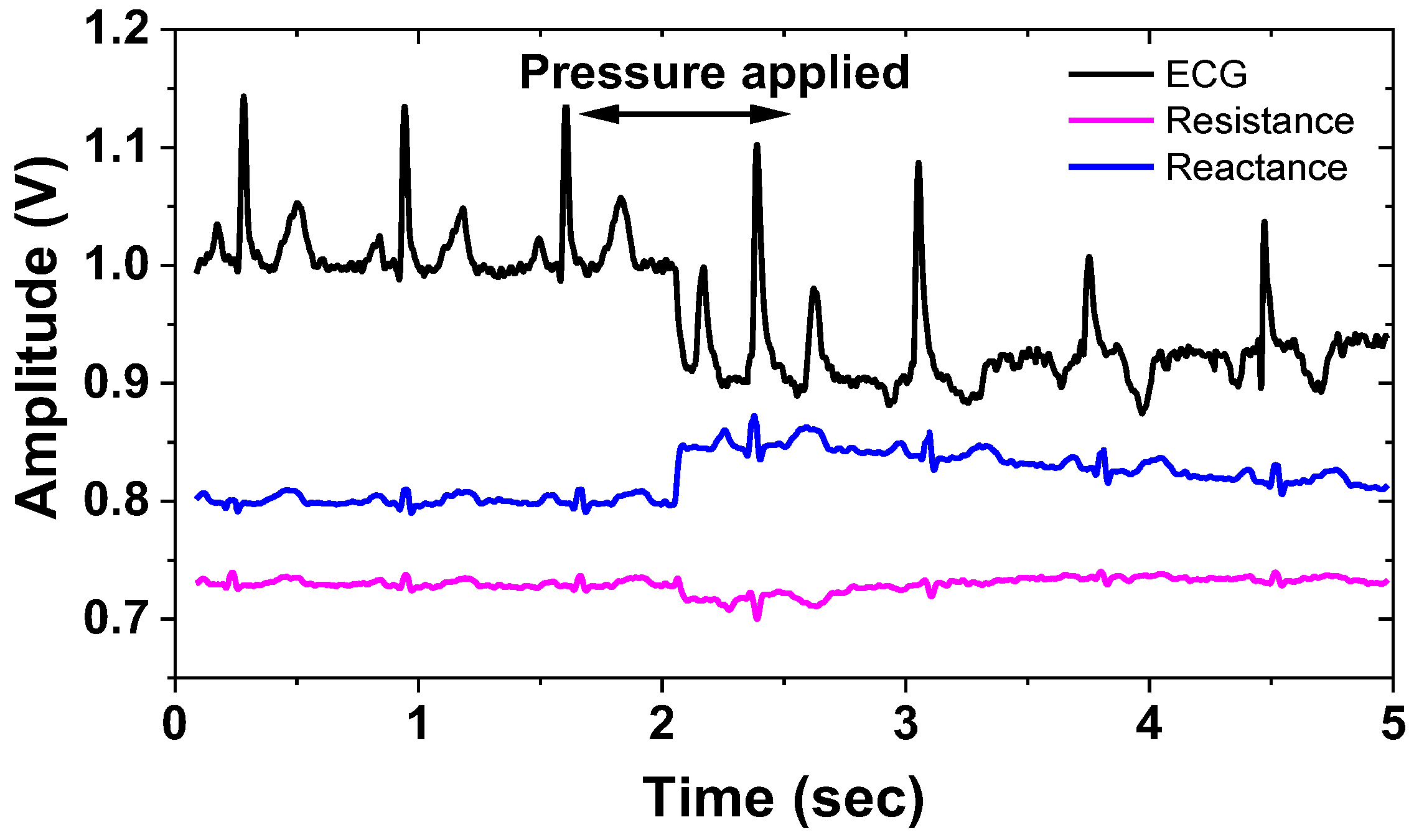
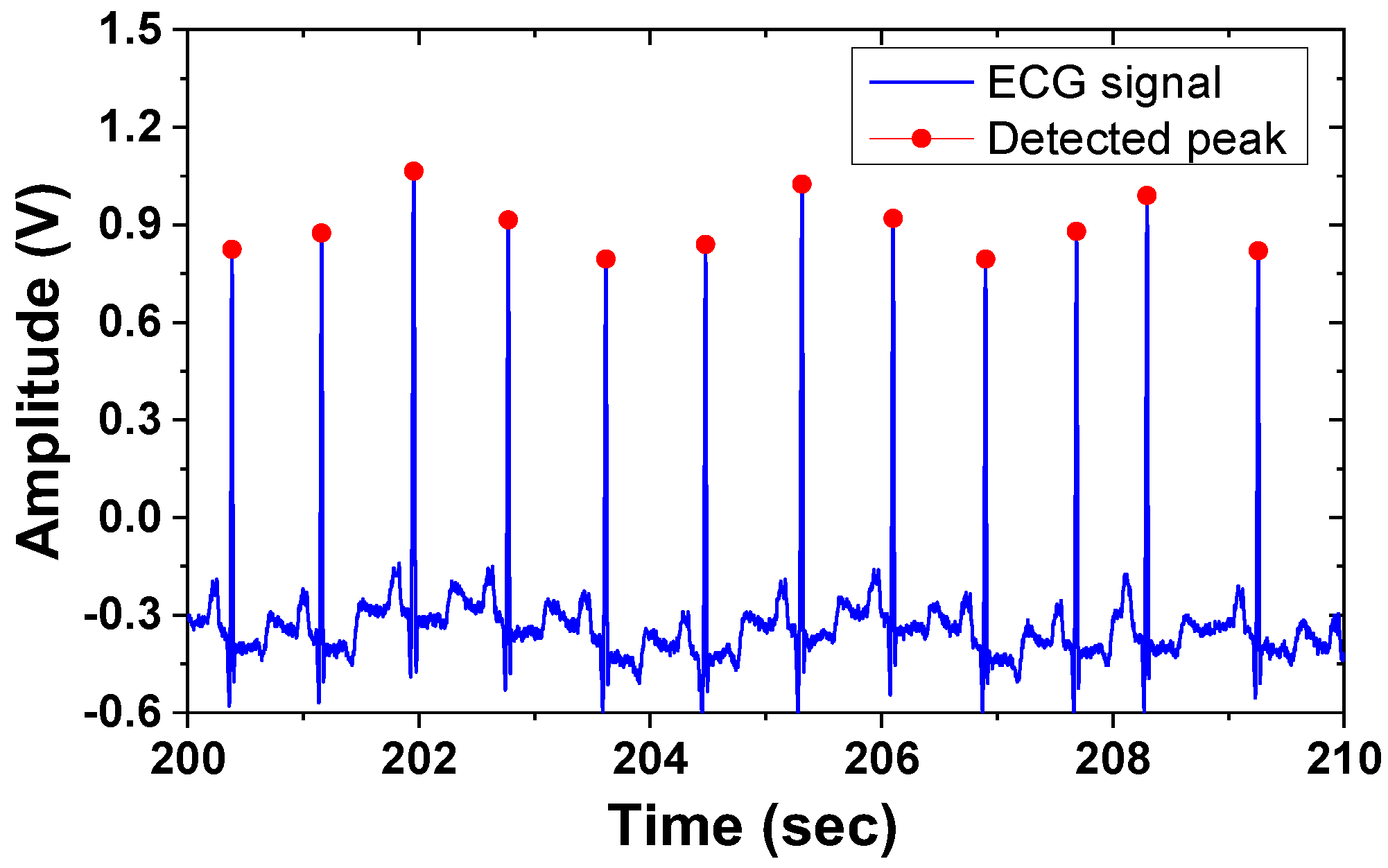
Figure 12 shows a block diagram of the BE signal processing IC. It consists of five channels for three types of measurements (ECG, BP, and IMP). Each channel includes an instrumentation amplifier (IA), a programmable gain amplifier (PGA), and a low-pass filter (LPF). The IC includes a multiphase clock generator, a bias generator/bandgap, and a multiplexer. The bias voltages are generated from the internal bandgap. The multiplexed outputs are digitized using a 12-b analog-to-digital converter (ADC) [22]. The ADC is implemented on a separate test board. The QRS peak detection and BP calculation are performed using a field programmable gate array (FPGA).
The BP channel extracts the information related to the QRS complex using the in-phase and quadrature chopping frequencies of fBPI = (fCH + Δf)(0°) and fBPQ = (fCH + Δf)(90°), respectively. The offset Δf is used to compensate for the channel delay. The IMP channel uses the in-phase and quadrature chopping frequencies of fIMPI = fAC(0°) and fIMPQ = fAC(90°), respectively, where fAC is the AC frequency of the current driver. The non-overlapping clocks are generated from the clock divider and multiphase clock generator. Because there is no input chopper in the IMP channel, the ECG signal is upmodulated to fAC at the IA output of the IMP channel, which is suppressed by the LPF [8]. If fAC = 4 kHz and fCH = 2 kHz is chosen, the signal input to the ECG and BP channels experiences two times frequency modulation, and the residual signals at 4 kHz and 8 kHz can be suppressed by the LPF.
Figure 13 shows the schematic of the IA using capacitive coupling. It consists of a folded-cascode amplifier (Gm5), re-used from the preamplifier (Figure 8) without the RRL input. The input and feedback capacitors (Cin1,2 and Cfb1,2) determine the closed-loop gain (Cin1,2/Cfb1,2), and the pseudo-resistors define the CM voltage.
Figure 14 shows the schematic of PGA. It consists of an operational transconductance amplifier (OTA), switches, and an array of capacitors. The first stage of the OTA uses a differential amplifier with internal positive feedback for gain boosting [15]. The second stage uses a common-source amplifier for increased output swing. The CMFB is implemented using a switched-capacitor (SC) network clocked by φ1 and φ2 [23]. When φ1 is high (φ2 is low), the amplifier operates in the negative feedback mode using the input capacitor (CIN) and the feedback capacitor (CFB). When φ2 is high (φ1 is low), it operates in CMFB mode using the CM input (VICM) and the output (VOCM). The low-frequency closed-loop gain (ACL) can be expressed as
A CL = A OL 1 + ( C FB / C IN ) A OL C IN C FB
where AOL is the open-loop gain of the OTA. The feedback capacitor is given by CFB = CU = 100 fF. The CIN is the capacitor sum connected to the input, which is determined by closed switches (S0–S2). The ACL is variable from 1 to 15 (v/v) by controlling the three switches.
Figure 15 shows the schematic of the LPF. Using the unit capacitor C = 100 fF, the states of the switches (S3–S6) determine the cutoff frequency. The number of SC stages determines the order of the filter. Figure 16 shows the simulated frequency responses of the LPFs. The ECG channel uses the first-order LPF to set the cutoff frequency close to 1.5 kHz. The IMP and BP channels use the second and third-order LPF to set the cutoff frequency at 60 Hz and 50 Hz, respectively.

5. Measured Results

Figure 17 shows the fabricated ICs for ECG/ETI system using the 180 nm CMOS process. The core size of the current driver and the preamplifier are 0.065 mm2 and 0.29 mm2, respectively. The core area of the BE signal processing IC is 0.9 mm2. The chips are mounted on three test boards for individual characterization using the chip-on-board (COB) technique. After functional testing, they are assembled for the ECG/ETI system characterization.
Figure 18 shows the measured transconductances of the current driver at 10 kHz using a load of (1 kΩ || 20 pF). The transconductance is relatively constant over the input range from −90 mV to +90 mV. Figure 19a shows the schematic of characterizing the output impedance ZOUT of the current driver. The differential input of the driver is generated using the Keysight 33500B with a high stability time base option. The output current is set to 200 μA by adjusting the input. The ZOUT value is obtained using two resistances (RL1 = 100 Ω, RL2 = 4.7 kΩ) and recording the change in the output voltage. The magnitude of ZOUT can be expressed as
| Z OUT | = | V L 2 V L 1 ( V L 2 / R L 2 ) ( V L 1 / R L 1 ) |
where VL1 and VL2 are measured voltages using RL1 and RL2, respectively [24]. The measured |ZOUT| is kept constant at 1 MΩ up to 500 kHz, reducing to 300 kΩ at 1 MHz. Figure 19b shows the measured output current as a function of frequency for three inputs. The injected current is measured using the voltage across a 100 Ω resistor, which is in series with the output load of (1 kΩ || 20 pF). For the input of 80 mVpp, the output current is relatively constant, up to 10 kHz, with a maximum error of 0.63%. The driver can operate up to 1 MHz, where the current is reduced to 0.13 mVpp. Figure 19c shows the output current as a function of load impedance. The data are measured at 100 Hz, and a current up to 600 μApp can be injected into the low impedance load using 120 mVpp.
Figure 20a shows the gain response (single-ended) of the preamplifier measured using a Keysight 35670A signal analyzer. The mid-band gain is 39.4 dB (differential) at 100 Hz by consuming 0.56 μA (including bias circuit) from VDD = 1.8 V. The mid-band common-mode rejection ratio (CMRR) and power-supply rejection ratio (PSRR) are 61 dB and 66 dB, respectively. Figure 20b shows the measured noise spectral density using fCH = 2 kHz. The input noise voltage density is 65 nV/√Hz with a 1/f corner frequency of 2.5 Hz. The integrated noise from 0.5 to 100 Hz is 1.14 μVrms.
Next, we present the measured result of BE signal processing IC. Figure 21 shows the measured gain control of the ECG channel. When all the switches of the PGA are in the OFF state, the mid-band gain is 20 dB. When all the switches are in the ON state, the PGA gain is 23 dB, which leads to an overall gain of 43 dB. Figure 22 shows the input noise density of the ECG channel measured using 40 dB gain by consuming 0.4 μA at 1.8 V. When the chopper is turned on, 1/f noise is effectively suppressed, resulting in a corner frequency of 2 Hz and noise density of 70 nV/√Hz. Figure 23 shows the amplified ECG signal for the input cardiac signal having Vpp = 12 mV (differential), generated from a function generator Keysight 33500B. The output shows Vpp = 600 mV (single-ended), indicating a 40 dB gain.
Figure 24 shows the measured results of the in-phase and quadrature IMP channels. The result is obtained by injecting current at three frequencies (fAC = 1, 4, and 5 kHz). The baseband output is observed when the demodulation chopper frequency is set to 5 kHz. The measured waveforms show that the output amplitude decreases with the increase in the capacitance value from 15 to 330 pF. Figure 25 shows the measured range of the ETI system. A resistor and a capacitor under the test are connected between the inputs of two AEs. When we use a sinusoidal current of 88 μApp at 1 kHz, the detection range using 69 dB channel gain is from 100 mΩ to 120 Ω. When the injected current is reduced to 215 nApp with the minimum PGA gain setting, the maximum range can be extended to 3 kΩ. The minimum range is extended to 10 mΩ using the maximum PGA gain. The simulated results agree well with the value of the reference resistance over the range. In the case of capacitance, the detection of the minimum value is limited by the parasitics of wiring capacitance in the test board. The measured linear range of capacitance is from 100 nF to 100 μF.
Figure 26 shows the measured results of the BP channels using a gain of 43 dB, fCH = 2 kHz, and ∆f = 50 Hz. The input cardiac signal having Vpp = 20 mV is generated using a function generator. Figure 27 shows the measured waveforms of the ECG and IMP channels. The electrodes attached to the wrists are connected to the current driver. A differential current of 303 μApp is injected into the electrode. Other sets of electrodes are connected between the body and test boards (AE and BE), thus amplifying the biopotential signal using 45 dB gain. The environmental noise is suppressed using a filtering function of the Keysight MSO-X oscilloscope. The motion artifact is induced by applying a hard push to the electrode. The result shows a successful operation of the proposed ETI system in vivo, where the ECG signals are measured while ETI is monitored.
Figure 28 shows the block diagram of the peak detection method based on Pan and Tompkins [25]. The magnitude of the signal derivative is processed through a moving-average filter. The detection threshold is set using the measured BP signal. The threshold detects the region of the QRS complexes. Additionally, a time domain search is performed around the detected beat to enhance the accuracy of locating the peak. Figure 29 shows the output of the processed waveform, indicating the successful detection of the ECG peaks. The power breakdown given in Table 1 shows that power consumption is dominated by the current driver. Table 2 shows the performance summary. The proposed ETI system is realized using a 1.26 mm2 (excluding ADC) consuming 3.6 mW from a 1.8 V single power supply.
Table 3 shows a comparison of the current drivers reported in the previous works [11,24,26,27,28]. In [26], electrical impedance tomography (EIT) for hand prosthesis control is proposed for the human-machine interface. The implemented IC uses a fully differential current driver and a current feedback IA, achieving a maximum output current of up to 1 mApp; however, the bandwidth (500 kHz) is lower than ours, and the THD (−42 dB or 0.79%) performance needs further improvement. Work [27] presents a current-conveyor-based current driver for EIT, achieving a wide bandwidth of up to 10 MHz. Targeted for EIT prostate and breast cancer detection, this work shows a high drive current of up to 1.2 mApp; however, the output impedance (101 kΩ) at 1 MHz is lower than ours. The two works [24,27] use a high supply (18 V and 3.3 V), increasing power consumption. Work [28] presents a current driver IC for a portable EIT system, achieving a relatively high output impedance (1 MΩ at 1 MHz) using a 1.2 V supply; however, the maximum output current is limited to 400 μApp with relatively high THD. The proposed driver features a high output impedance (1 MΩ) and operates at a low supply (1.8 V) suitable for portable system applications.
Table 4 shows a comparison of the system with other works [29,30,31,32]. Work [29] presents a low-power (0.221 mW) readout IC using a digital-assisted baseline impedance cancellation technique, providing an extended frequency (1 MHz) measurement; however, the impedance range and resolution are lower than ours. In [30], a six-channel EIT system for portable breast cancer detection is proposed and validated in a wearable setting. The system provides a good signal-to-noise (SNR) of up to 90 dB; however, the impedance range is not shown, and it consumes a relatively high power (53.4 mW). Work [31] presents a high input impedance, low noise ETI sensor system using a current mismatch cancellation technique, achieving a relatively good resolution (0.5 mΩ) and low power (0.128 mW); however, the current is limited to 100 μApp demanding a high gain, high power preamplifier. Work [32] is a commercial system with a balanced impedance range, resolution, and power consumption. Compared to other works, the proposed system achieves the lowest minimum impedance value, a relatively good resolution, and a high driver current. The system is realized using 3.6 mW power suitable for portable applications.

6. Conclusions

This paper presents an active-electrode ECG/ETI sensor system using a wideband low-noise IA and a high-impedance current driver. The balanced current driver uses a matched current source and sink, which operate under negative feedback to increase the output impedance. To increase the linear input range, a new source degeneration method is proposed. The measured output impedance of the driver is 1 MΩ and 300 kΩ at 500 kHz and 1 MHz, respectively. The AFFC technique is applied for the preamplifier to achieve a wide bandwidth using a small Miller compensation capacitor. The proposed IA achieves a noise density and 1/f noise corner of 65 nV/√Hz and 2.5 Hz, respectively. The BE signal processing IC is designed for three types of signal monitoring (ECG, BP, and IMP). The measured results show that the output of the BP channel is successfully used for real-time detection of the QRS complex in the ECG signal. Using the gain programmability, the detection range of the IMP channel is increased from 25 to 43 dB. The resistance detection range is from 10 mΩ to 3 kΩ, and the capacitive range is from 100 nF to 100 μF. Characterizing the complete system shows successful detection of the motion artifact while measuring the ECG/ETI using 3.6 mW.

Author Contributions

X.T.N. designed the circuit, performed the experimental work, and wrote the manuscript. M.A. edited the manuscript. J.-W.L. conceived the project, organized the paper content, and edited the manuscript. All authors have read and agreed to the published version of the manuscript.

Funding

This work was supported in part by the Basic Science Research Program through the National Research Foundation of Korea (No. 2021R1A2B5B01001475) and in part by National R&D Program through the National Research Foundation of Korea, funded by the Ministry of Science and ICT (No. 2020M3H2A1076786).

Institutional Review Board Statement

Not applicable.

Acknowledgments

The chip fabrication and CAD tools were supported by the IDEC (IC Design Education Center).

Conflicts of Interest

The authors declare no conflict of interest.

Appendix A

We consider the denominator of Equation (4) to find the poles as
s 3 R 1 R L C m 1 C m 2 C L + s 2 R 1 R L C m 2 ( C L g m a + C m 1 g m 2 ) + s R 1 R L g m 2 g m a ( C m 1 + C m 2 ) + g m a = 0 .
Case 1: in the case of ( C L g m a < < C m 1 g m 2 ), Equation (A1) can be written as
s 3 R 1 R L C m 1 C m 2 C L + s 2 R 1 R L C m 2 C m 1 g m 2 + s R 1 R L g m 2 g m a ( C m 1 + C m 2 ) + g m a = 0 ,
where the three poles can be expressed as
p 0 d 0 d 1 = 1 R 1 R L g m 2 ( C m 1 + C m 2 ) ,
p 1 d 1 d 2 = R 1 R L g m 2 g m a ( C m 1 + C m 2 ) R 1 R L C m 2 C m 1 g m 2 = g m a ( C m 1 + C m 2 ) C m 2 C m 1 ,
p 2 d 2 d 3 = R 1 R L C m 2 C m 1 g m 2 R 1 R L C m 1 C m 2 C L = g m 2 C L .
Case 2: In the case of ( C L g m a > > C m 1 g m 2 ), Equation (A1) can be written as
s 3 R 1 R L C m 1 C m 2 C L + s 2 R 1 R L C m 2 C L g m a + s R 1 R L g m 2 g m a ( C m 1 + C m 2 ) + g m a = 0 .
where the three poles can be expressed as
p 0 d 0 d 1 = 1 R 1 R L g m 2 ( C m 1 + C m 2 ) ,
p 1 d 1 d 2 = R 1 R L g m 2 g m a ( C m 1 + C m 2 ) R 1 R L C m 2 C L g m a = g m 2 ( C m 1 + C m 2 ) C m 2 C L ,
p 2 d 2 d 3 = R 1 R L C m 2 C L g m a R 1 R L C m 1 C m 2 C L = g m a C m 1 .
The expression of p1 given by Equation (A8) is proportional to the root mean square of the current. When the load current changes, increasing p1 can affect the value of p2, creating complex poles. We assume |s|>>|p1| when considering the non-dominant poles, p1 and p2. Then, the approximate values of p1 and p2 can be obtained by solving the following equation as
s 2 R 1 R L C m 1 C m 2 C L + s R 1 R L C m 2 C L g m a + R 1 R L g m 2 g m a ( C m 1 + C m 2 ) = 0 .
The above result can be further simplified as
s 2 C m 1 C m 2 C L + s C m 2 C L g m a + g m 2 g m a ( C m 1 + C m 2 ) = 0 .
with the determinant of
Δ = C m 2 C L g m a [ C m 2 C L g m a 4 C m 1 g m 2 ( C m 1 + C m 2 ) ]
and we obtain the expression for complex conjugate poles as
p 1 , 2 = s = C m 2 C L g m a ± j C m 2 C L g m a [ C m 2 C L g m a 4 C m 1 g m 2 ( C m 1 + C m 2 ) ] 2 C m 1 C m 2 C L .
The above result can be further simplified as
p 1 , 2 = s = g m a 2 C m 1 ± j g m a [ C m 2 C L g m a 4 C m 1 g m 2 ( C m 1 + C m 2 ) ] 4 C m 1 2 C m 2 C L .
The Q-factor of the non-dominant poles is obtained as
Q = | p 1 , 2 | 2 | Re { p 1 , 2 } | = 1 4 + C m 2 C L g m a 4 C m 1 g m 2 ( C m 1 + C m 2 ) 4 C m 2 C L g m a
where the magnitude can be expressed as
| p 1 , 2 | = g m a 2 4 C m 1 2 + g m a [ C m 2 C L g m a 4 C m 1 g m 2 ( C m 1 + C m 2 ) ] 4 C m 1 2 C m 2 C L .

References

  1. Halter, R.J.; Hartov, A.; Heaney, J.A.; Paulsen, K.D.; Schned, A.R. Electrical impedance spectroscopy of the human prostate. IEEE Trans. Biomed. Eng. 2007, 54, 1321–1327. [Google Scholar] [CrossRef] [PubMed]
  2. Moganti, G.L.K.; Siva Praneeth, V.N.; Vanjari, S.R.K. A hybrid bipolar active charge balancing technique with adaptive electrode tissue interface (ETI) impedance variations for facial paralysis patients. Sensors 2022, 22, 1756. [Google Scholar] [CrossRef] [PubMed]
  3. Marcôndes, D.W.C.; Paterno, A.S.; Bertemes-Filho, P. Parasitic effects on electrical bioimpedance systems: Critical review. Sensors 2022, 22, 8705. [Google Scholar] [CrossRef]
  4. Chi, Y.M.; Jung, T.P.; Cauwenberghs, G. Dry-contact and noncontact biopotential electrodes: Methodological review. IEEE Rev. Biomed. Eng. 2010, 3, 106–119. [Google Scholar] [CrossRef] [Green Version]
  5. Matthews, R.; Turner, P.J.; McDonald, N.J.; Ermolaev, K.; Mc Manus, T.; Shelby, R.A.; Steindorf, M. Real time workload classification from an ambulatory wireless EEG system using hybrid EEG electrodes. In Proceedings of the 2008 30th Annual International Conference of the IEEE Engineering in Medicine and Biology Society, Vancouver, BC, Canada, 20–25 August 2008; pp. 5871–5875. [Google Scholar]
  6. Dozio, R.; Baba, A.; Assambo, C.; Burke, M.J. Time based measurement of the impedance of the skin-electrode interface for dry electrode ECG recording. In Proceedings of the 2007 29th Annual International Conference of the IEEE Engineering in Medicine and Biology Society, Lyon, France, 22–26 August 2007; pp. 5001–5004. [Google Scholar]
  7. Nishimura, S.; Tomita, Y.; Horiuchi, T. Clinical application of an active electrode using an operational amplifier. IEEE Trans. Biomed. Eng. 1992, 39, 1096–1099. [Google Scholar] [CrossRef]
  8. Xu, J.; Mitra, S.; Matsumoto, A.; Patki, S.; van Hoof, C.; Makinwa, K.A.A.; Yazicioglu, R. A wearable 8-channel active-electrode EEG/ETI acquisition system for body area networks. IEEE J. Solid-State Circuits 2014, 49, 2005–2016. [Google Scholar] [CrossRef] [Green Version]
  9. Nuwer, M.R.; Comi, G.; Emerson, R.; Fuglsang-Frederiksen, A.; Guérit, J.-M.; Hinrichs, H.; Ikeda, A.; Luccas, J.C.; Rappelsburger, P. IFCN standards for digital recording of clinical EEG. Electroencephalogr. Clin. Neurophysiol. 1998, 106, 259–261. [Google Scholar] [CrossRef]
  10. Jochum, T.; Denison, T.; Wolf, P. Integrated circuit amplifiers for multi-electrode intracortical recording. J. Neural Eng. 2009, 6, 012001. [Google Scholar] [CrossRef]
  11. Constantinou, L.; Bayford, R.; Demosthenous, A. A wideband low-distortion CMOS current driver for tissue impedance analysis. IEEE Trans. Circuits Syst. II Express Briefs 2015, 62, 154–158. [Google Scholar] [CrossRef]
  12. Franco, S. Design with Operational Amplifiers and Analog Integrated Circuits; McGraw-Hill: New York, NY, USA, 2003. [Google Scholar]
  13. Zhang, F.; Teng, Z.; Zhong, H.; Bertemes-Filho, P.; Wilson, A.J. A comparison of modified Howland circuits as current generators with current mirror type circuits. Physiol. Meas. 2000, 21, 1–6. [Google Scholar]
  14. Avestruz, A.T.; Santa, W.; Carlson, D.; Jensen, R.; Stanslaski, S.; Helfenstine, A.; Denison, T. A 5 μw/channel spectral analysis IC for chronic bidirectional brain-machine interfaces. IEEE J. Solid-State Circuits 2008, 43, 3006–3024. [Google Scholar] [CrossRef]
  15. Lee, H.S.; Nguyen, V.N.; Pham, X.L.; Lee, J.W.; Park, H.K. A 250-μW, 18-nV/rtHz current-feedback chopper instrumentation amplifier in 180-nm CMOS for high-performance bio-potential sensing applications. Analog Int. Circuits Signal Process. 2017, 90, 137–148. [Google Scholar] [CrossRef]
  16. Schreier, R.; Silva, J.; Steensgaard, J.; Temes, G.C. Design-oriented estimation of thermal noise in switched-capacitor circuits. IEEE Trans. Circuits Syst. I Regul. Pap. 2005, 52, 2358–2368. [Google Scholar] [CrossRef]
  17. Cheng, Q.; Zhang, H.; Xue, L.; Guo, J. A 1.2-V 43.2-μW three-stage amplifier with cascode miller-compensation and Q-reduction for driving large capacitive load. In Proceedings of the 2016 IEEE International Symposium on Circuits and Systems, Montréal, QC, Canada, 22–25 July 2016; pp. 458–461. [Google Scholar]
  18. Guo, S.; Lee, H. Dual active-capacitive-feedback compensation for low-power large-capacitive-load three-stage amplifiers. IEEE J. Solid-State Circuits 2011, 46, 452–464. [Google Scholar] [CrossRef]
  19. Lee, H.; Mok, P.K.T. Active-feedback frequency-compensation technique for low-power multistage amplifiers. IEEE J. Solid-State Circuits 2003, 38, 511–520. [Google Scholar] [CrossRef] [Green Version]
  20. Vo, D.H.T.; Lee, J.W. Analysis and design of a low power regulator for a fully integrated HF-band passive RFID tag IC. Analog Integr. Circuits Signal Process. 2012, 71, 69–80. [Google Scholar] [CrossRef]
  21. Pham, X.T.; Duong, D.N.; Nguyen, N.T.; van Truong, N.; Lee, J.W. A 4.5 GΩ-input impedance chopper amplifier with embedded DC-servo and ripple reduction loops for impedance boosting to sub-Hz. IEEE Trans. Circuits Syst. II Express Briefs 2021, 68, 116–120. [Google Scholar] [CrossRef]
  22. Nguyen, C.L.; Phan, H.N.; Lee, J.W. A 12-b subranging SAR ADC using detect-and-skip switching and mismatch calibration for biopotential sensing applications. Sensors 2022, 22, 3600. [Google Scholar] [CrossRef] [PubMed]
  23. Razavi, B. Design of Analog CMOS Integrated Circuits; McGraw-Hill: New York, NY, USA, 2001. [Google Scholar]
  24. Constantinou, L.; Triantis, I.F.; Bayford, R.; Demosthenous, A. High-power CMOS current driver with accurate transconductance for electrical impedance tomography. IEEE Trans. Biomed. Circuits Syst. 2014, 8, 575–583. [Google Scholar] [CrossRef] [PubMed]
  25. Pan, J.; Tompkins, W.J. A real-time QRS detection algorithm. IEEE Trans. Biomed. Eng. 1985, BME-32, 230–236. [Google Scholar] [CrossRef]
  26. Wu, Y.; Jiang, D.; Liu, X.; Bayford, R.; Demosthenous, A. A human-machine interface using electrical impedance tomography for hand prosthesis control. IEEE Trans. Biomed. Circuits Syst. 2018, 12, 1322–1333. [Google Scholar] [CrossRef] [PubMed] [Green Version]
  27. Rao, A.J.; Murphy, E.K.; Shahghasemi, M.; Odame, K.M. Current-conveyor-based wideband current driver for electrical impedance tomography. Physiol. Meas. 2019, 40, 034005. [Google Scholar] [CrossRef] [Green Version]
  28. Jang, J.; Kim, M.; Bae, J.; Yoo, H.J. A 2.79-mW 0.5%-THD CMOS current driver IC for portable electrical impedance tomography system. In Proceedings of the 2017 IEEE Asian Solid-State Circuits Conference (A-SSCC), Seoul, South Korea, 6–8 November 2017; pp. 145–148. [Google Scholar]
  29. Ha, H.; Sijbers, W.; Wegberg, R.V.; Xu, J.; Konijnenburg, M.; Vis, P.; Breeschoten, A.; Song, S.; Hoof, C.V.; van Helleputte, N.A. A bio-impedance readout IC with digital-assisted baseline cancellation for two-electrode measurement. IEEE J. Solid-State Circuits 2019, 54, 2969–2979. [Google Scholar] [CrossRef]
  30. Hong, S.; Lee, K.; Ha, U.; Kim, H.; Lee, Y.; Kim, Y.; Yoo, H.J. A 4.9 MΩ-sensitivity mobile electrical impedance tomography IC for early breast-cancer detection system. IEEE J. Solid-State Circuits 2015, 50, 245–257. [Google Scholar] [CrossRef]
  31. Pan, Q.; Qu, T.; Tang, B.; Shan, F.; Hong, Z.; Xu, J. A 0.5-mΩ/rtHz dry-electrode bioimpedance interface with current mismatch cancellation and input impedance of 100 MΩ at 50 kHz. IEEE J. Solid-State Circuits 2022. early access. [Google Scholar] [CrossRef]
  32. Texas Instruments, AFE4300, Low-Cost, Integrated Analog Frontend for Weight-Scale and Body Composition Measurement. Available online: https://www.ti.com/lit/ds/symlink/afe4300.pdf (accessed on 9 December 2022).
Figure 1. Block diagram for the ECG/ETI measurement system.
Sensors 23 02536 g001
Figure 2. Schematic of electrode-tissue impedance (ETI) measurement.
Sensors 23 02536 g002
Figure 3. Schematic of the balanced current driver.
Sensors 23 02536 g003
Figure 4. Source degeneration method using (a) conventional and (b) proposed approach. (c) Comparison of the transfer characteristics.
Sensors 23 02536 g004
Figure 5. Schematic of the differential difference amplifier. Circuits for source degeneration is shown in blue color. (W/L)3A,3B = (W/L)6A,6B = 1 μm/0.7 μm. Rb1,b2 is realized using a diode-connected transistor having a size of (W/L) = 0.9 μm /0.7 μm. Cb1,b2 = 0.32 pF.
Sensors 23 02536 g005
Figure 6. Schematic of the transconductor.
Sensors 23 02536 g006
Figure 7. Schematic of the CCIA using active feedback frequency compensation (AFFC) and ripple-reduction loop (RRL). Cin1,2 = 15 pF, Cfb1,2 = 0.14 pF.
Sensors 23 02536 g007
Figure 8. Schematic of the folded-cascode amplifier with common-mode feedback.
Sensors 23 02536 g008
Figure 9. Equivalent small-signal circuit of the amplifier for calculating the open-loop gain.
Sensors 23 02536 g009
Figure 10. Comparison of the open-loop gain of the amplifier using AFFC and traditional Miller compensation.
Sensors 23 02536 g010
Figure 11. Schematic showing the operation of the ripple-reduction loop.
Sensors 23 02536 g011
Figure 12. Block diagram of the back-end signal processing IC. The spectrums of the ECG and IMP channels are shown in the inset.
Sensors 23 02536 g012
Figure 13. Schematic of the instrumentation amplifier.
Sensors 23 02536 g013
Figure 14. Schematic of the PGA.
Sensors 23 02536 g014
Figure 15. Schematic of the low-pass filter.
Sensors 23 02536 g015
Figure 16. Simulated frequency responses of the low-pass filters.
Sensors 23 02536 g016
Figure 17. Microphotograph of (a) current driver, (b) preamplifier, (c) back-end signal processing IC.
Sensors 23 02536 g017
Figure 18. Measure transconductances as a function of input voltage.
Sensors 23 02536 g018
Figure 19. (a) Schematic of characterizing the output impedance. (b) Measured output current as a function of frequency under different inputs. (c) Measured output current as a function of load impedance under different inputs.
Sensors 23 02536 g019aSensors 23 02536 g019b
Figure 20. (a) Measured gain of the CCIA, (b) measured input-referred noise voltage spectral density of the CCIA for the active electrode.
Sensors 23 02536 g020aSensors 23 02536 g020b
Figure 21. Measured frequency response of the ECG channel for eight gain settings.
Sensors 23 02536 g021
Figure 22. Measured input-referred noise voltage spectral density of the ECG channel.
Sensors 23 02536 g022
Figure 23. Measured amplified ECG signal.
Sensors 23 02536 g023
Figure 24. Measured result of the impedance channel. The current driver injects input at three frequencies (1 kHz, 4 kHz, and 5 kHz). The demodulation is performed at 5 kHz.
Sensors 23 02536 g024
Figure 25. Measured range of the ETI system for (a) differential resistance and (b) differential capacitance. The values of the injected current are also shown.
Sensors 23 02536 g025
Figure 26. Measured result of band power channels. Positive and negative inputs are indicated with blue and red lines, and output is indicated with black lines.
Sensors 23 02536 g026
Figure 27. Measured waveforms of the ECG and IMP channels.
Sensors 23 02536 g027
Figure 28. Flowchart of the ECG peak detection algorithm.
Sensors 23 02536 g028
Figure 29. Waveforms of the ECG signal and detected peaks.
Sensors 23 02536 g029
Table 1. Power breakdown.
Current driver1.98 mA @ 1.8 V = 3.56 mW
Preamplifier0.4 μA (core), 0.16 μA (bias) @ 1.8 V = 1 μW
Back-end3.7 μA @ 1.8 V= 6.6 μW (ECG: 0.5 μA, ETI: 1.1 μA, BP: 1.1 μA)
Total3.6 mW
Table 2. Performance Summary.
Process0.18 μm CMOS
Active electrodeCurrent driverFrequency1 MHz (max)
Amplitude600 μApp
Size0.065 mm2
PreamplifierGain39.4 dB (differential)
Input noise density65 nV/√Hz
Integrated noise1.14 μVrms (100 Hz)
Size0.29 mm2
Back-endNumber of channels5
Gain23–43 dB
Bandwidth0.5–1 kHz
Input noise density70 nV/√Hz
Size0.9 mm2
Table 3. Comparison of the current driver.
[11][24][26][27][28]This Work
Bandwidth1 MHz500 kHz500 kHz10 MHz1 MHz1 MHz
Output
impedance
1 MΩ
@ 500 kHz/
360 kΩ
@ 1 MHz
1 MΩ
@ 100 kHz/
500 kΩ
@ 500 kHz
750 kΩ
@ 500 kHz
101 kΩ
@ 1 MHz/
19.5 kΩ
@ 10 MHz
1 MΩ
@1 MHz
1 MΩ
@ 500 kHz/
300 kΩ
@ 1 MHz
Max. output
current
1 mApp5 mApp1 mApp1.2 mApp400 μApp>500 μApp
THD<0.1% *
@ 1 mApp
0.69%
@ 5 mApp
0.79%
@ 3.97 mApp
0.14% *
@ 1.2 mApp
<0.5%
@ 400 μApp
0.29% **
@ 303 μApp
Supply±2.5 V18 V±1.65 V3.3 V1.2 V1.8 V
* Increases to 0.68% at 10 MHz. ** Measured using driver current less than maximum value at 50 kHz.
Table 4. Comparison of system performance.
This Work[29][30][31][32]
Frequency (kHz)1001–1000100100150
IMP range (Ω)0.01–3 k100–2 k-20–4 k2.8 k
Resolution
(mΩrms)
3.52–144.90.514.9
Current (μApp)600 100 400 100667
ModulationSineSquareSineSquarePseudo-sine
Power (mW)3.60.22153.40.1282.9
Disclaimer/Publisher’s Note: The statements, opinions and data contained in all publications are solely those of the individual author(s) and contributor(s) and not of MDPI and/or the editor(s). MDPI and/or the editor(s) disclaim responsibility for any injury to people or property resulting from any ideas, methods, instructions or products referred to in the content.

