A Review of Thin-Film Magnetoelastic Materials for Magnetoelectric Applications


 , ,
, ,
Abstract
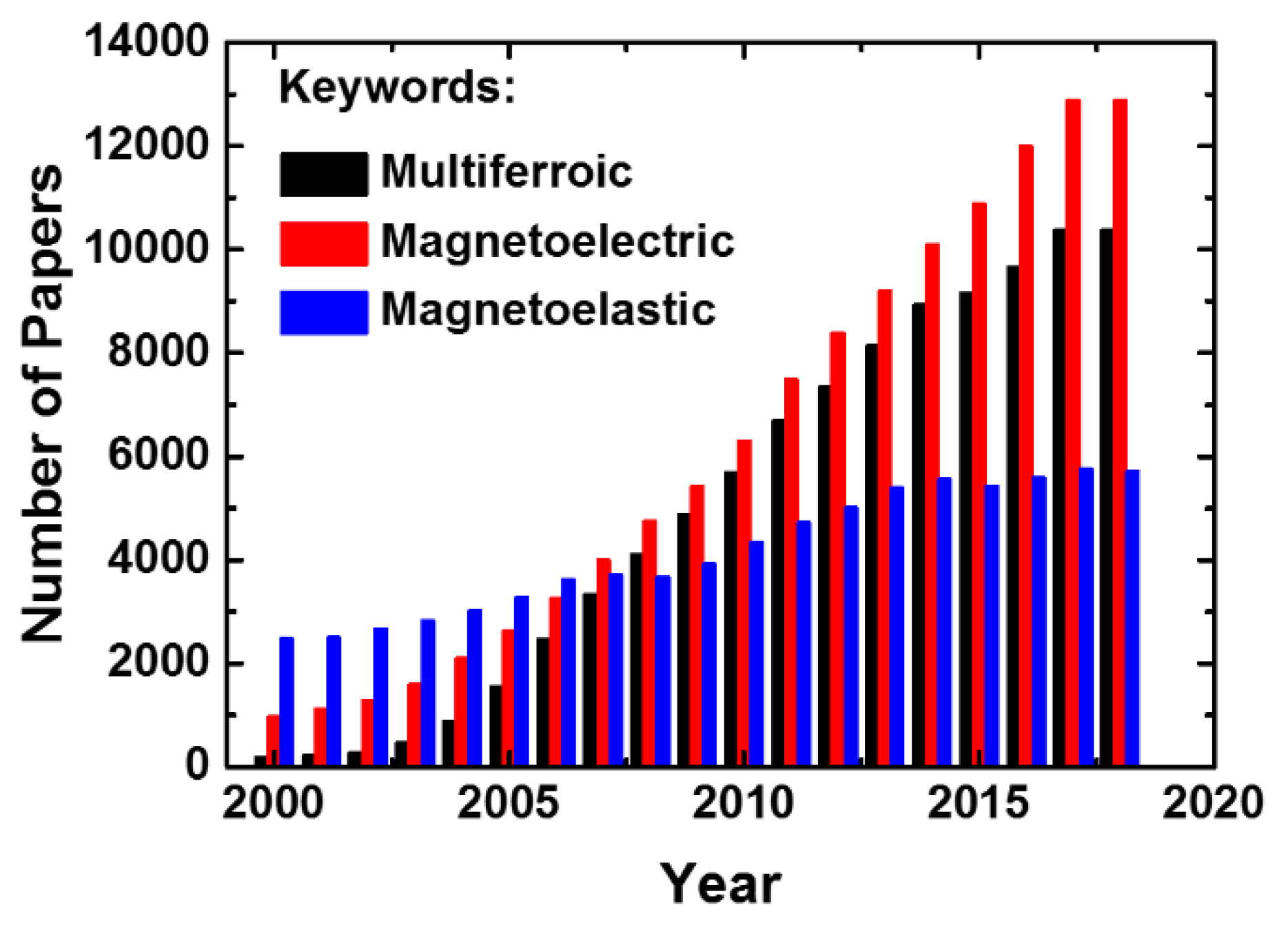
:1. Introduction
1.1. Multiferroic Materials
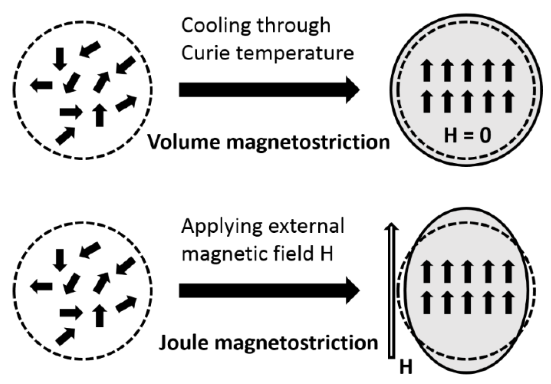
1.2. Magnetoelastic Materials
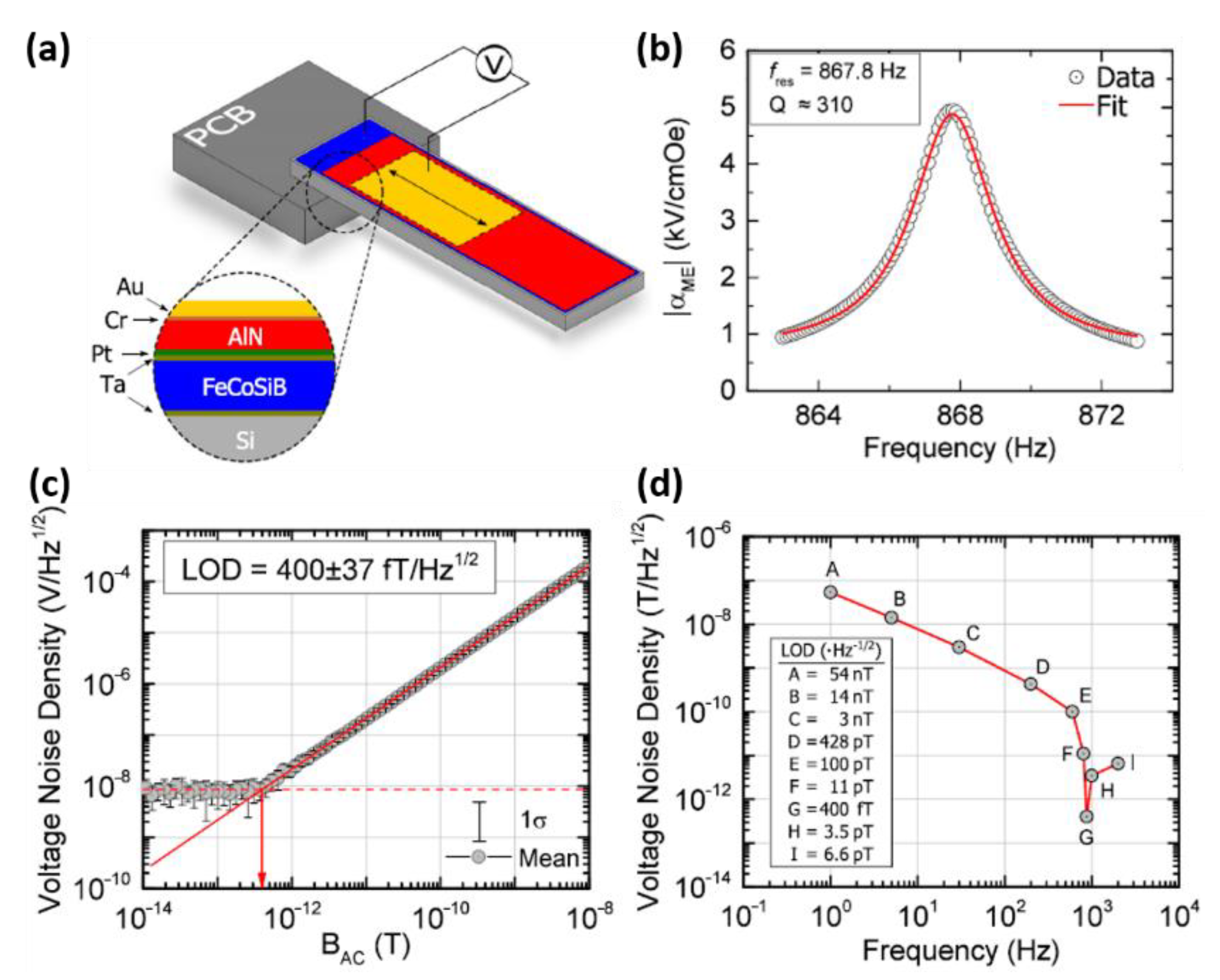
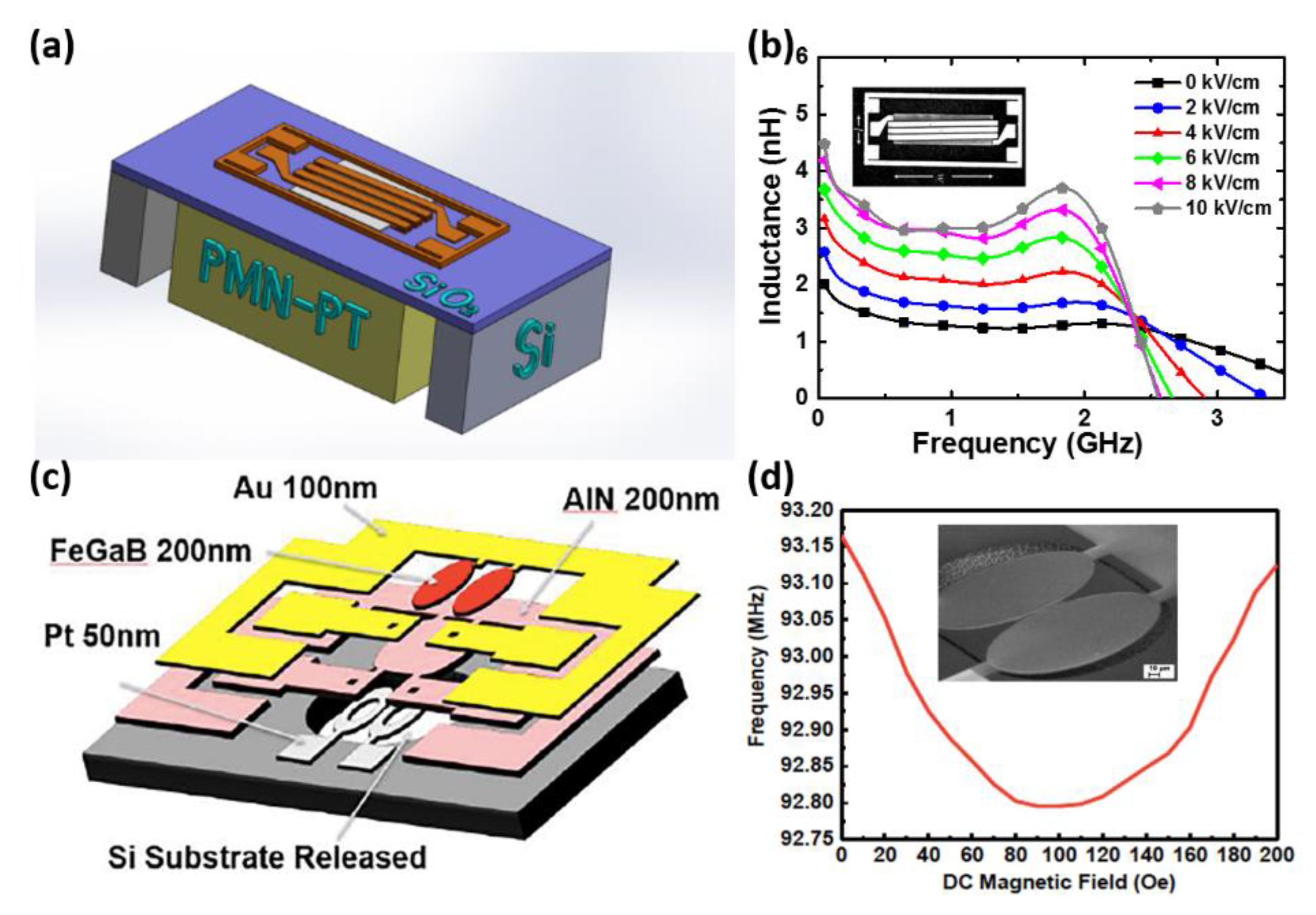
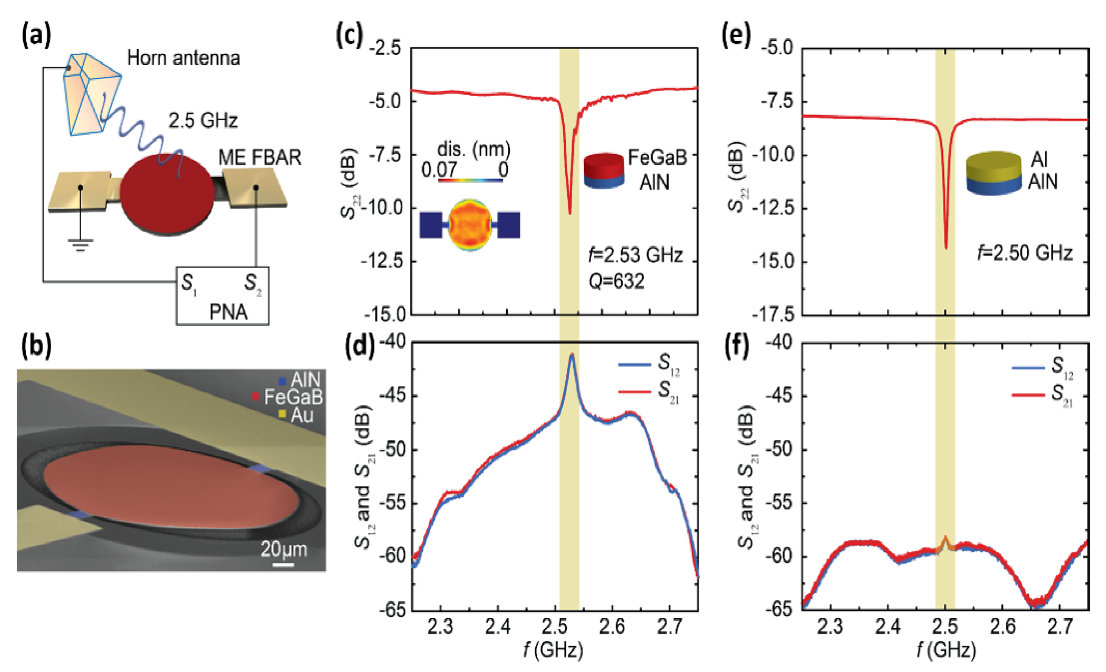
1.3. Magnetoelectric Applications
2. Fabrication and Characterization Methods
2.1. Fabrication Techniques of Thin Films
2.2. Characterization Methods of Thin Films
3. Magnetostrictive Thin Films
3.1. Rare-Earth-Transition Metal Inter-Metallics
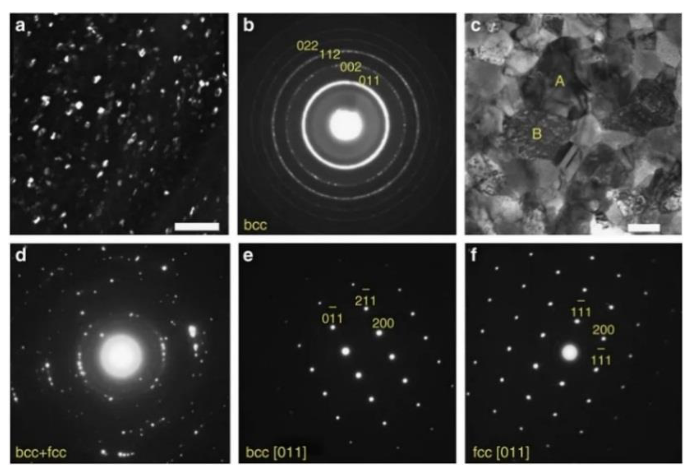
3.1.1. TbDyFe
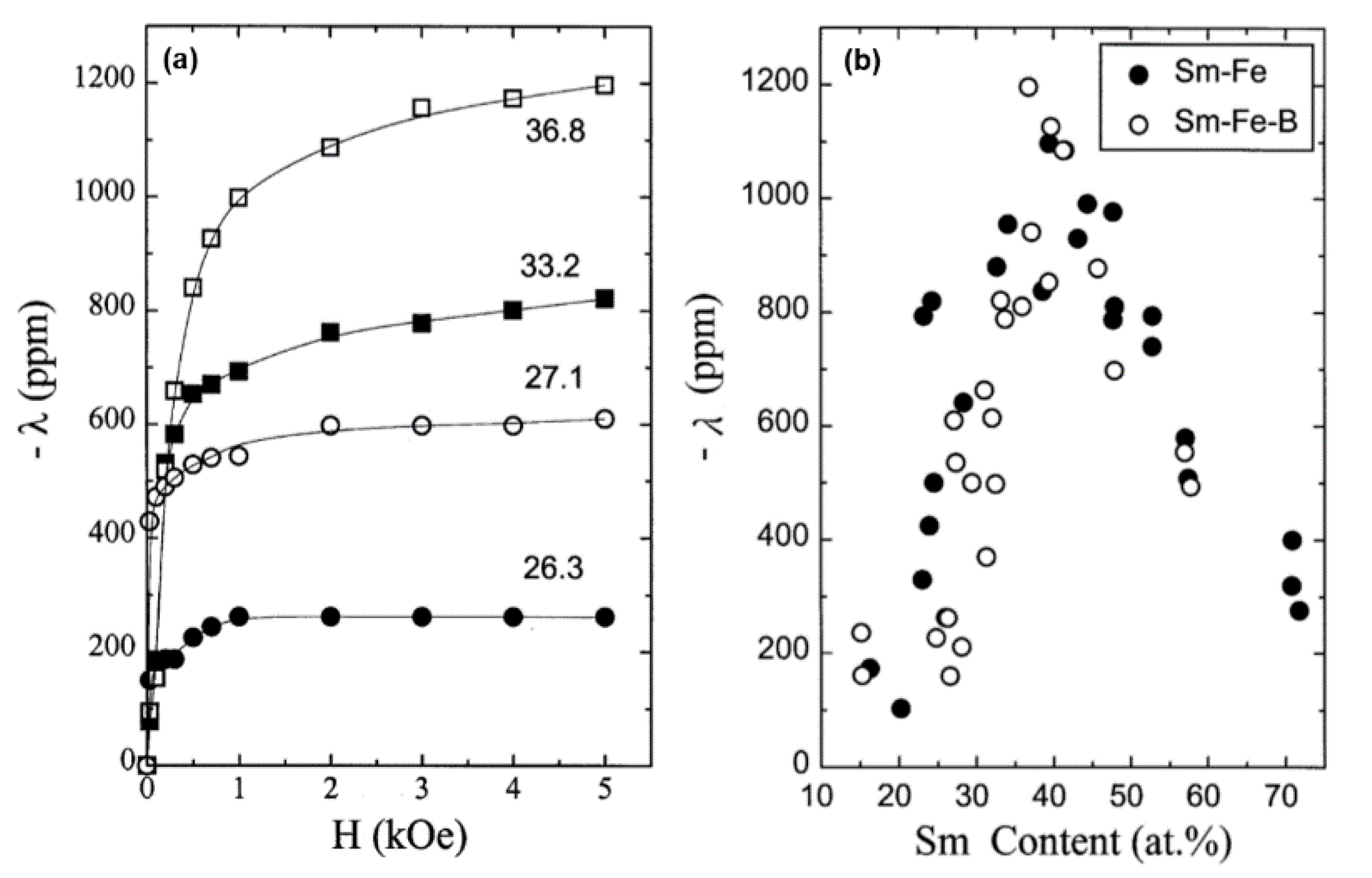
3.1.2. SmFe and SmFeB
3.2. Rear-Earth-Free Alloys
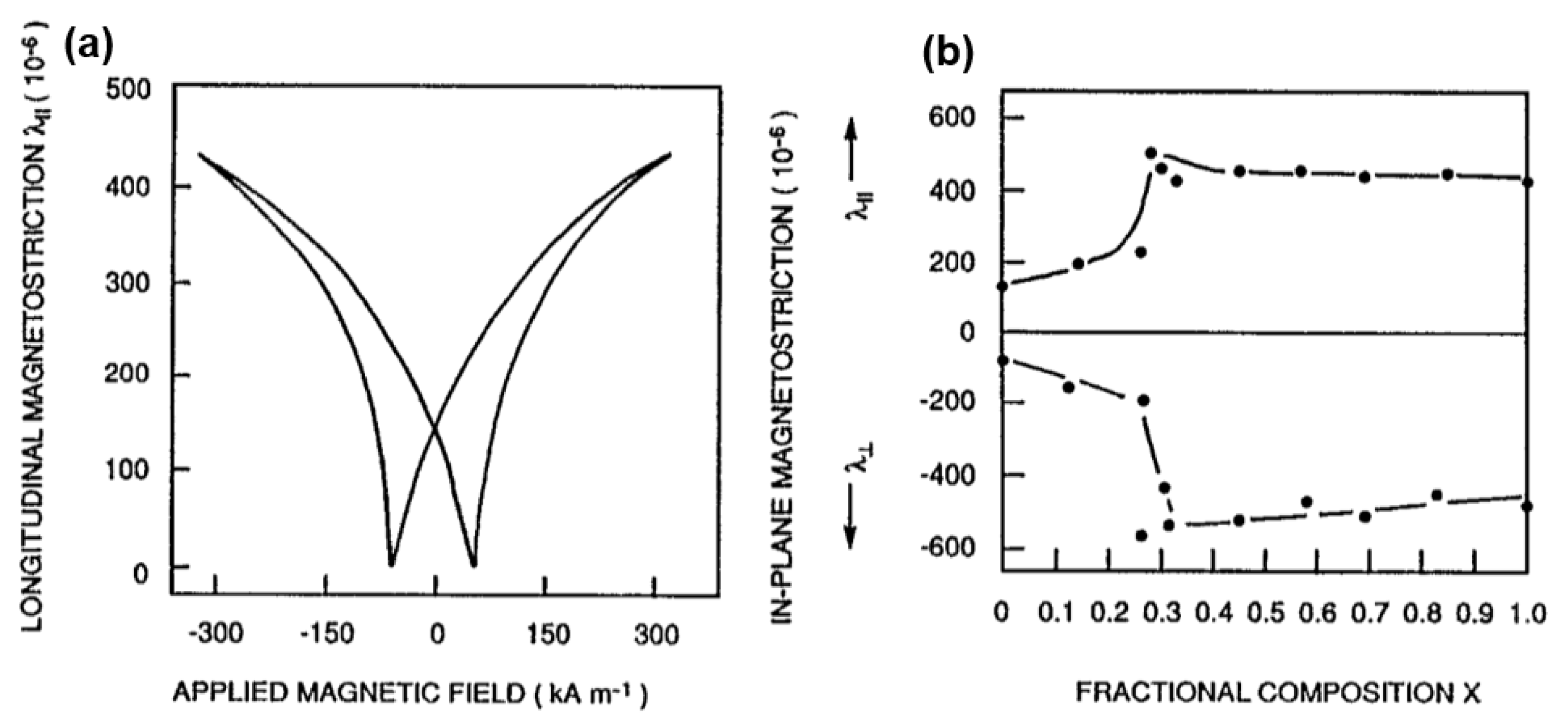
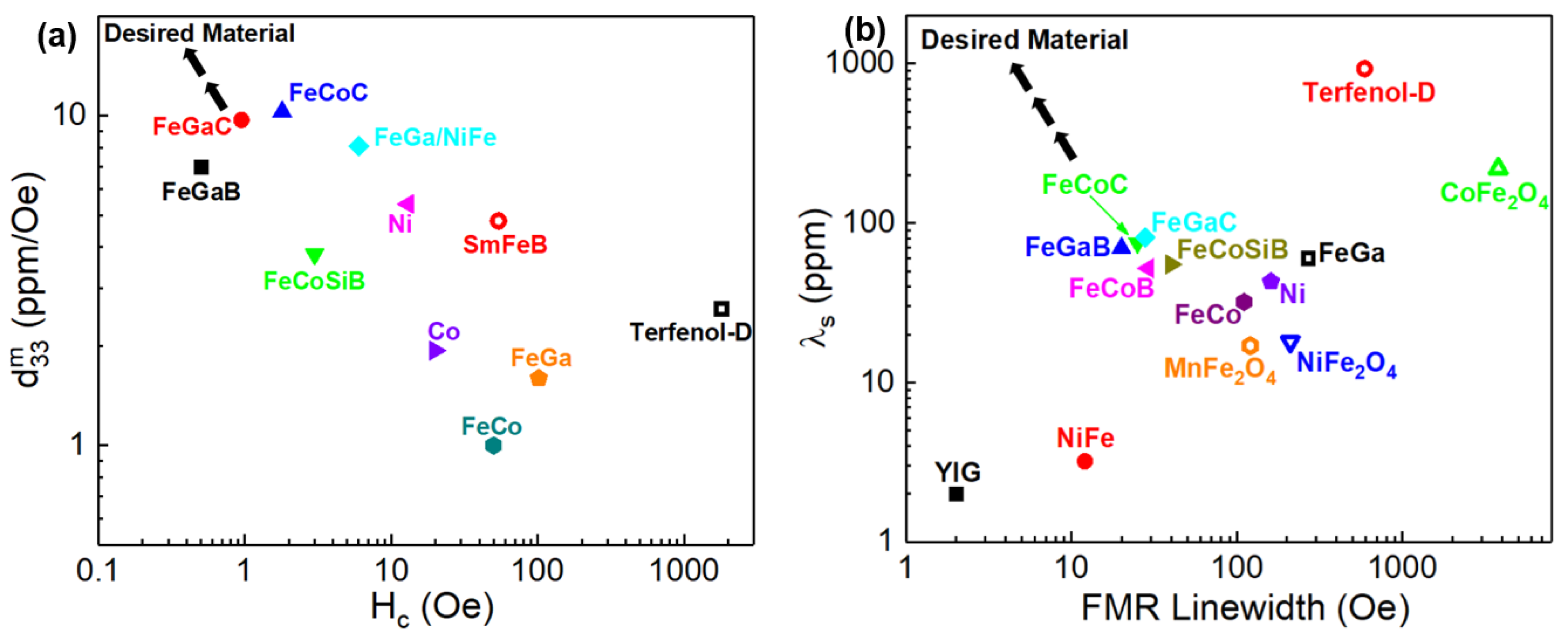
3.2.1. FeGa Based Alloy
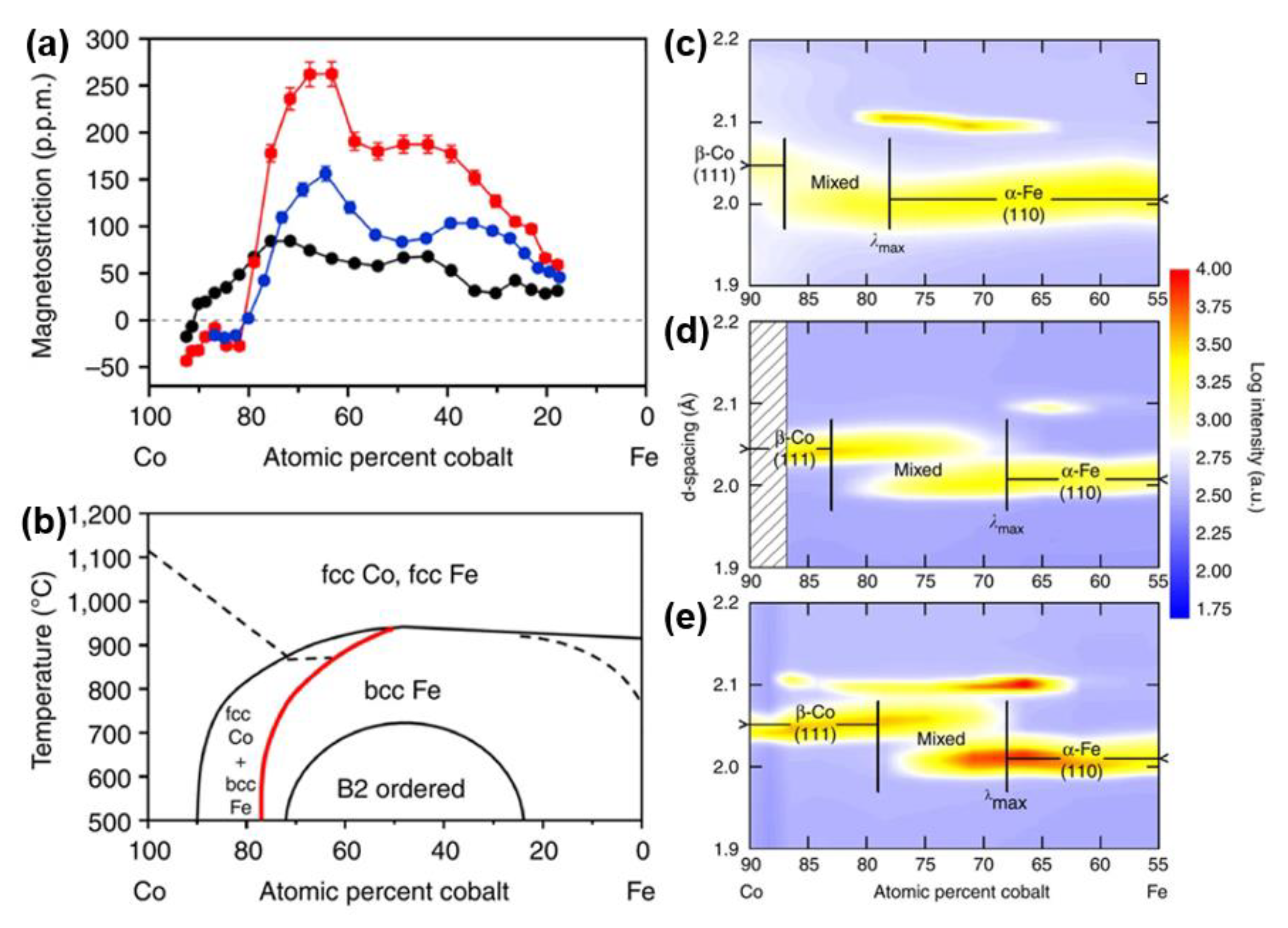
3.2.2. FeCo Based Alloys
3.3. Exchange Coupling in Multilayers
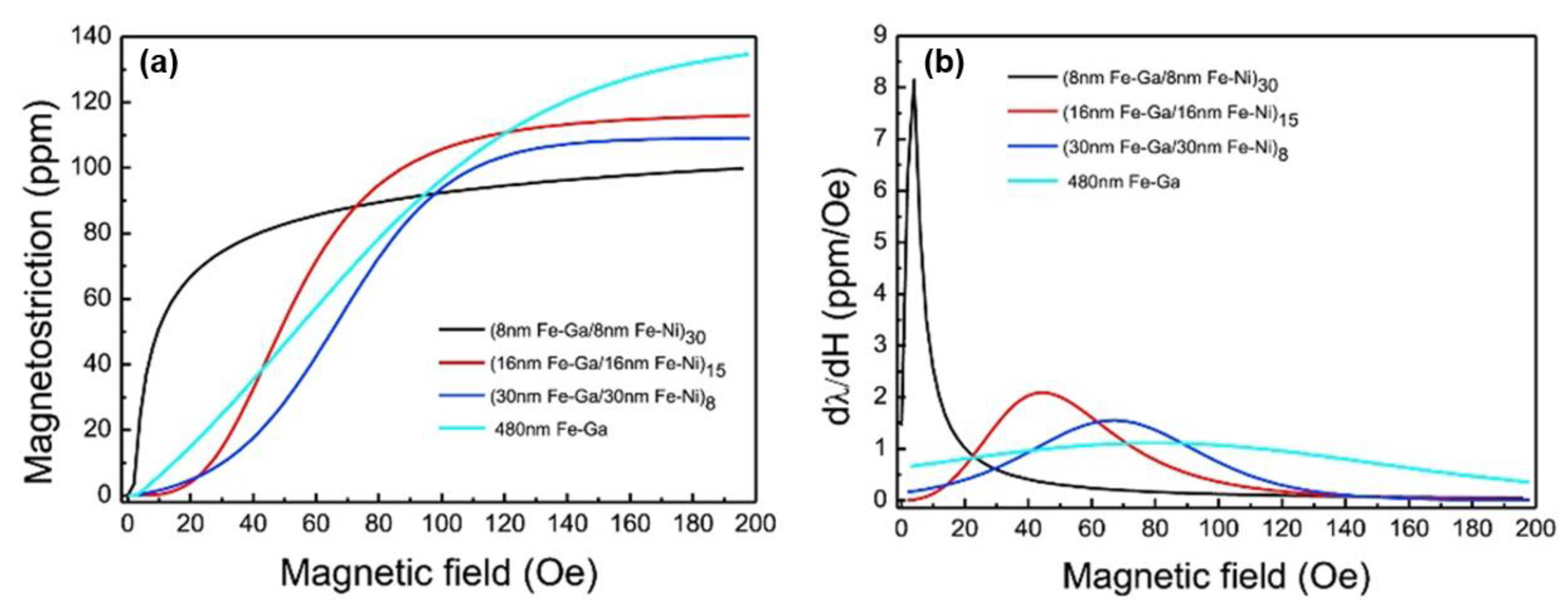
3.3.1. FeGa/NiFe Multilayers
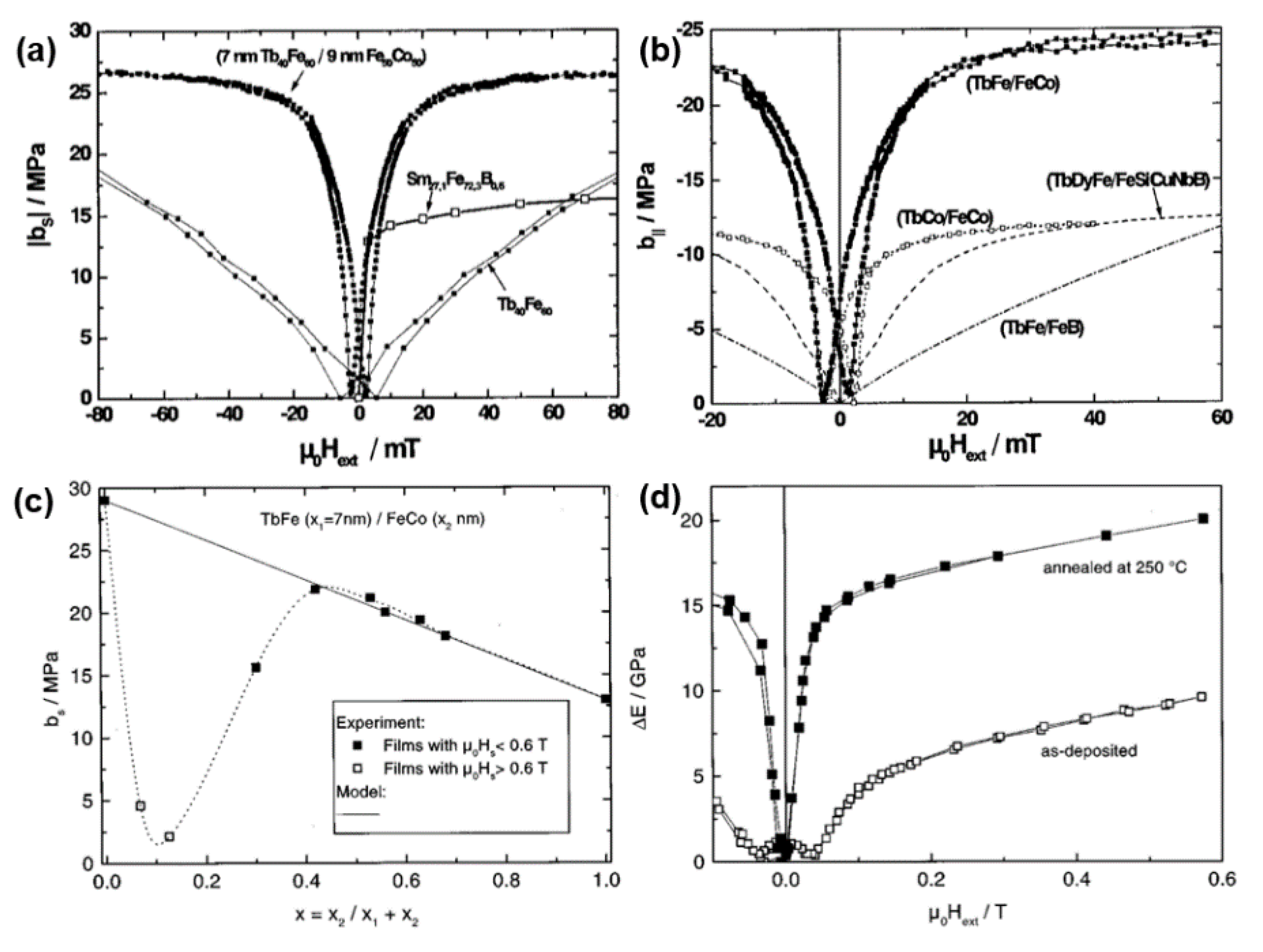
3.3.2. TbFe/FeCo Multilayers
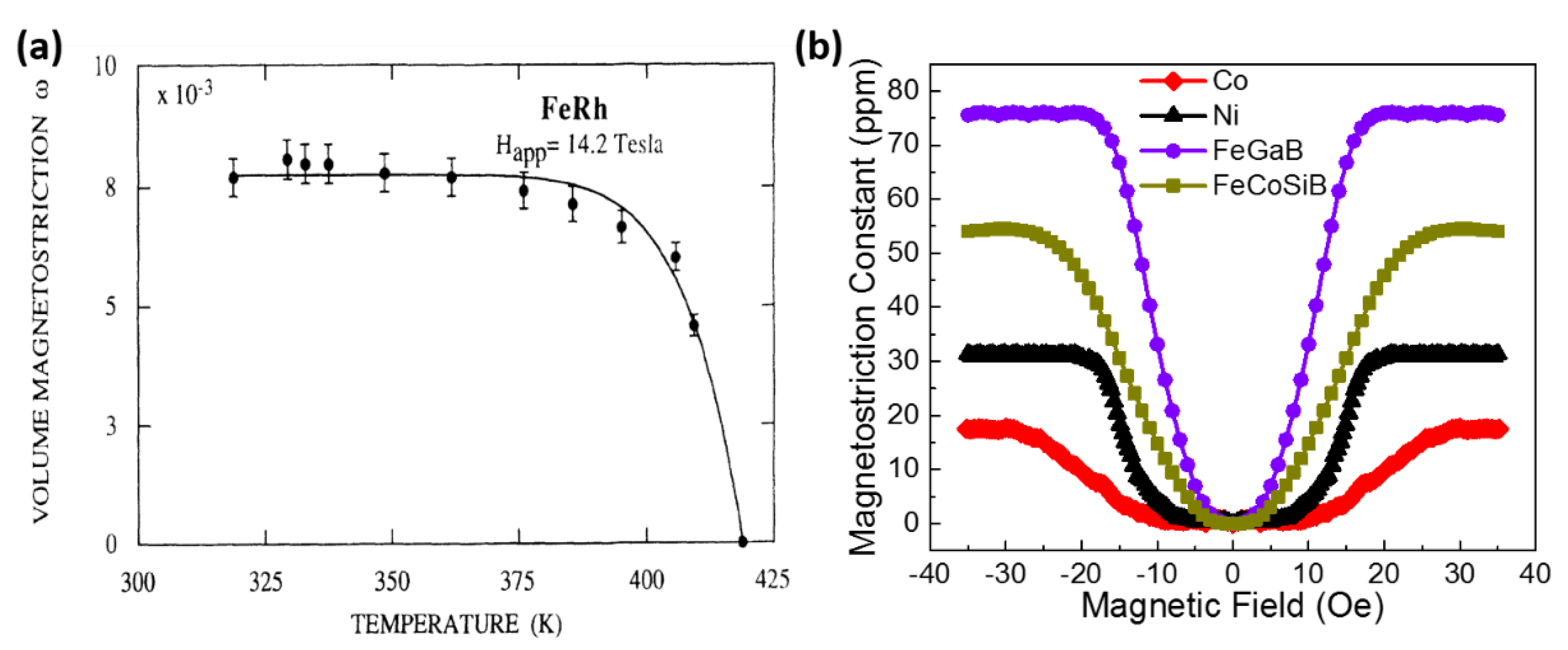
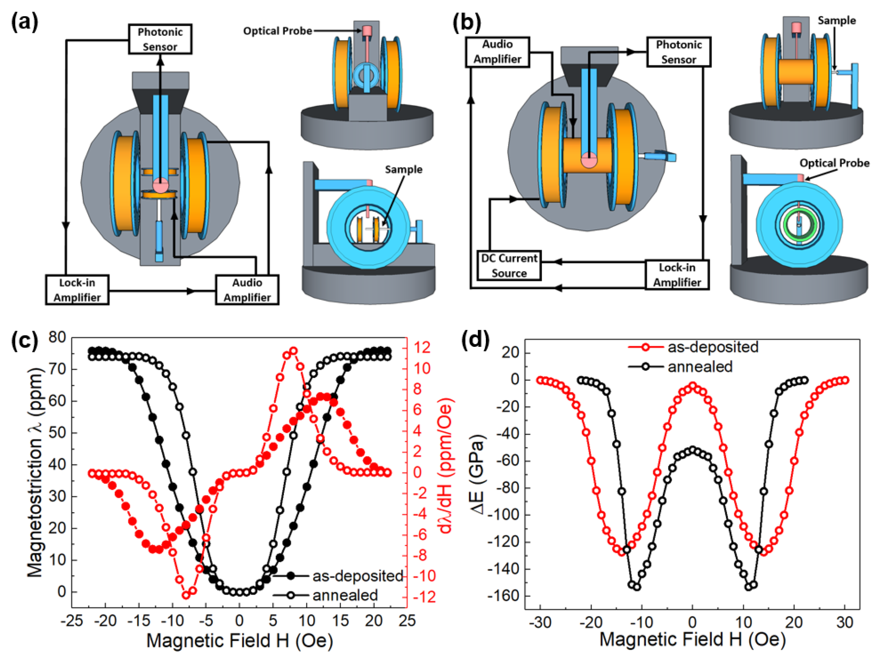
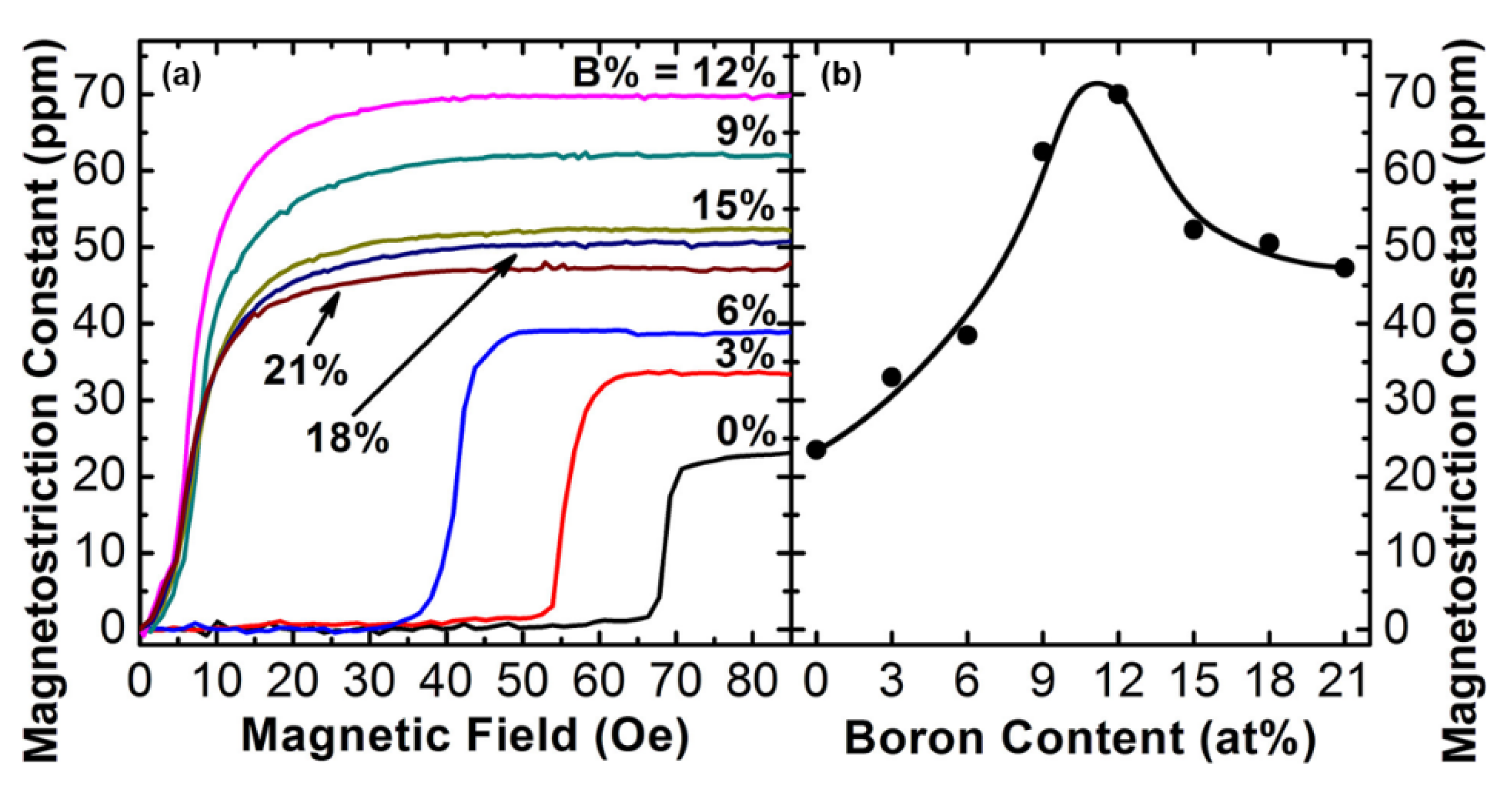
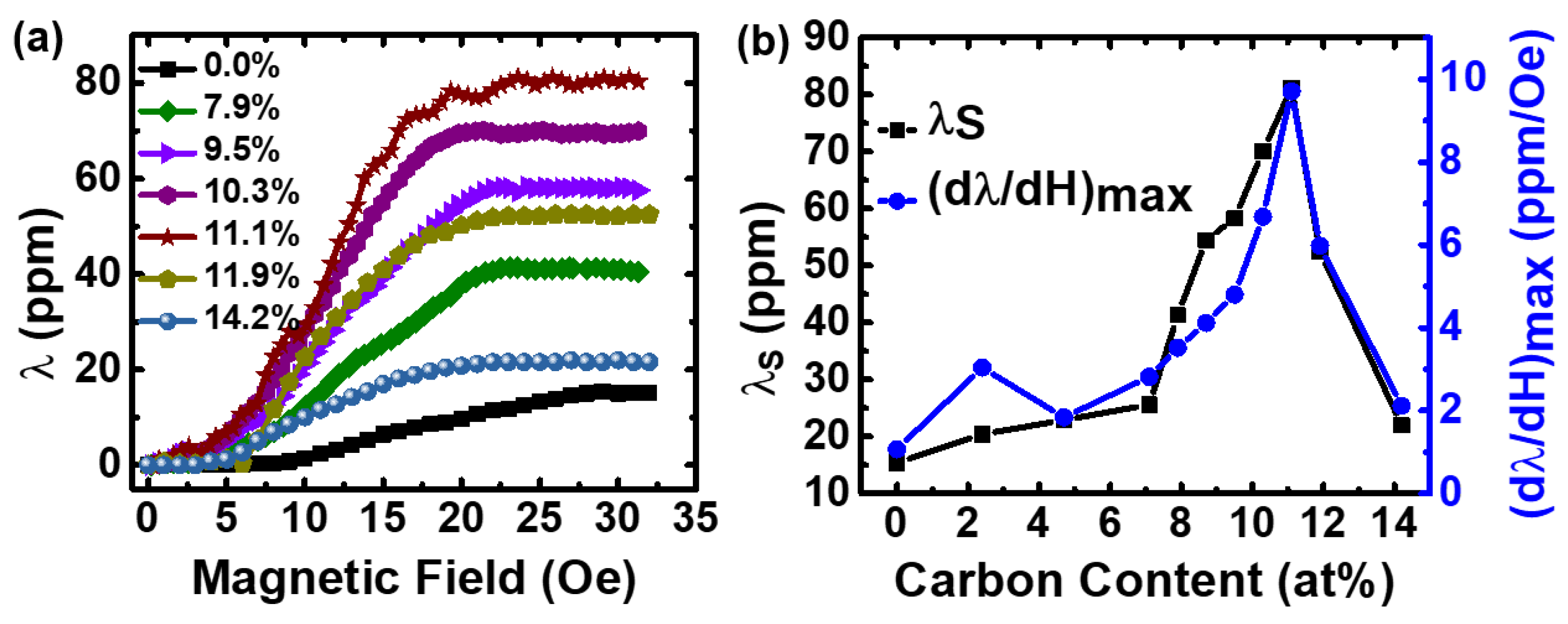
3.4. Heat Treatment on Magnetostrictive Thin Films
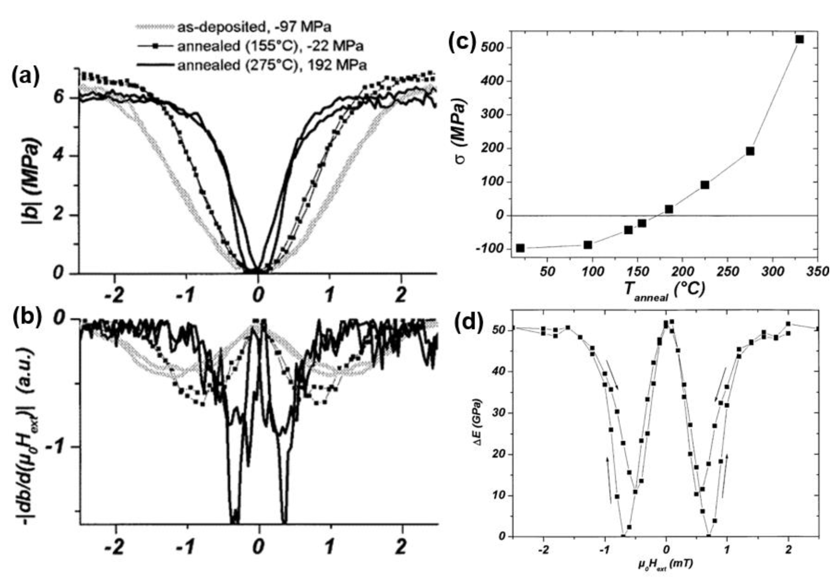
3.4.1. Stress Release by Post Annealing
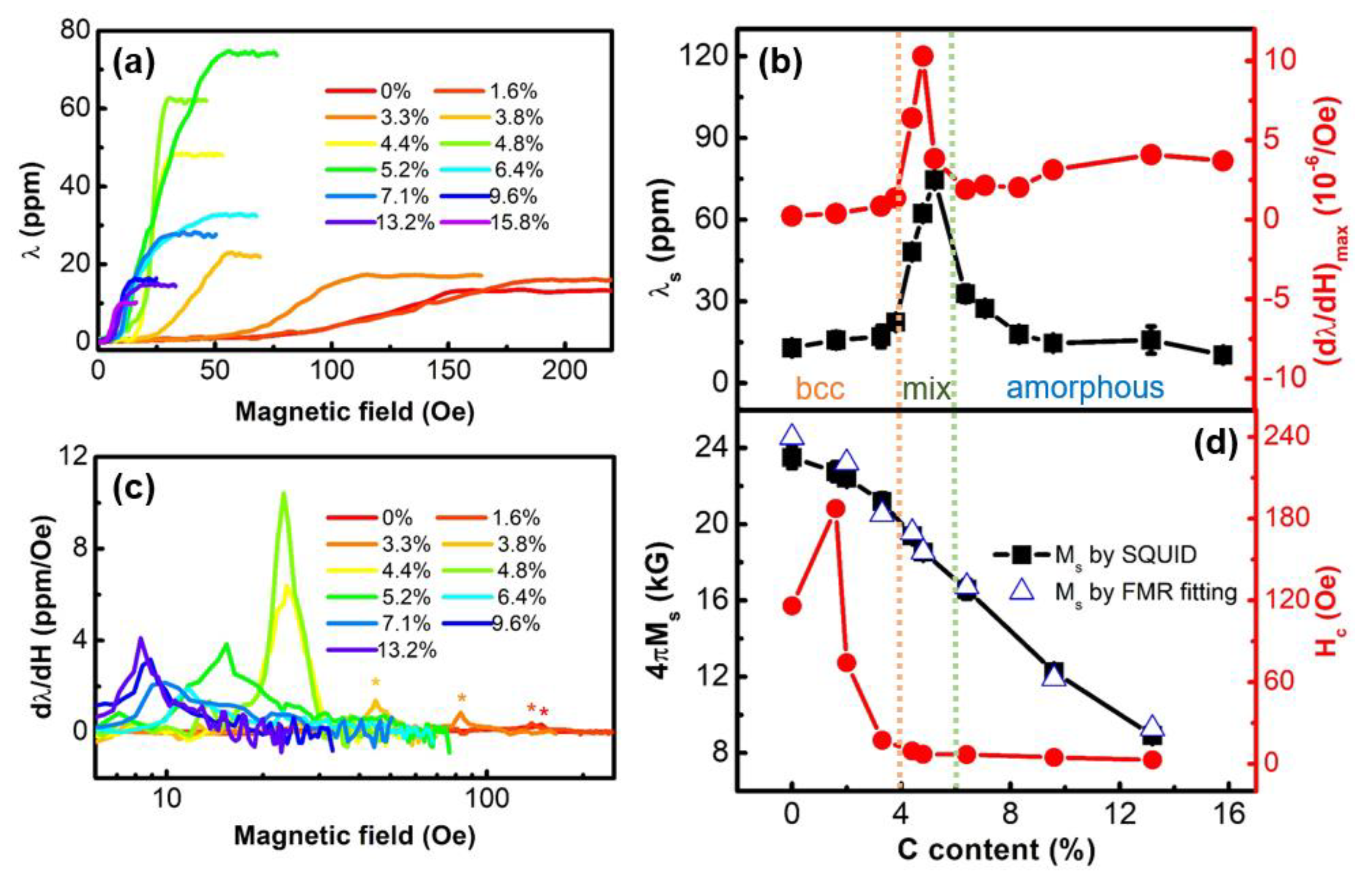
3.4.2. Phase Boundary Changes by Cooling Processes
4. Summary and Conclusions
Funding
Acknowledgments
Conflicts of Interest
References
- Nan, C.-W.; Bichurin, M.; Dong, S.; Viehland, D.; Srinivasan, G. Multiferroic magnetoelectric composites: Historical perspective, status, and future directions. J. Appl. Phys. 2008, 103, 1. [Google Scholar] [CrossRef]
- Ma, J.; Hu, J.; Li, Z.; Nan, C.W. Recent progress in multiferroic magnetoelectric composites: From bulk to thin films. Adv. Mater. 2011, 23, 1062–1087. [Google Scholar] [CrossRef] [PubMed]
- Srinivasan, G. Magnetoelectric composites. Annu. Rev. Mater. Res. 2010, 40, 153–178. [Google Scholar] [CrossRef]
- Sun, N.X.; Srinivasan, G. Voltage Control of Magnetism in Multiferroic Heterostructures and Devices; World Scientific Publishing Company: Singapore, 2013; Volume 2, p. 1240004. [Google Scholar] [CrossRef]
- Ramesh, R.; Spaldin, N.A. Multiferroics: Progress and prospects in thin films. Nat. Mater. 2007, 6, 21. [Google Scholar] [CrossRef] [PubMed]
- Spaldin, N.; Ramesh, R. Advances in magnetoelectric multiferroics. Nat. Mater. 2019, 18, 203. [Google Scholar] [CrossRef]
- Palneedi, H.; Annapureddy, V.; Priya, S.; Ryu, J. Status and perspectives of multiferroic magnetoelectric composite materials and applications. Actuators 2016, 5, 9. [Google Scholar] [CrossRef] [Green Version]
- Chu, Z.; PourhosseiniAsl, M.; Dong, S. Review of multi-layered magnetoelectric composite materials and devices applications. J. Phys. D: Appl. Phys. 2018, 51, 243001. [Google Scholar] [CrossRef]
- Eerenstein, W.; Mathur, N.; Scott, J.F. Multiferroic and magnetoelectric materials. Nature 2006, 442, 759. [Google Scholar] [CrossRef]
- Fiebig, M. Revival of the magnetoelectric effect. J. Phys. D: Appl. Phys. 2005, 38, R123. [Google Scholar] [CrossRef]
- Spaldin, N.A.; Fiebig, M. The renaissance of magnetoelectric multiferroics. Science 2005, 309, 391–392. [Google Scholar] [CrossRef]
- Martin, L.; Chu, Y.-H.; Ramesh, R. Advances in the growth and characterization of magnetic, ferroelectric, and multiferroic oxide thin films. Mater. Sci. Eng.: R: Rep. 2010, 68, 89–133. [Google Scholar] [CrossRef] [Green Version]
- Tu, C.; Chu, Z.-Q.; Spetzler, B.; Hayes, P.; Dong, C.-Z.; Liang, X.-F.; Chen, H.-H.; He, Y.-F.; Wei, Y.-Y.; Lisenkov, I. Mechanical-Resonance-Enhanced Thin-Film Magnetoelectric Heterostructures for Magnetometers, Mechanical Antennas, Tunable RF Inductors, and Filters. Materials 2019, 12, 2259. [Google Scholar] [CrossRef] [PubMed] [Green Version]
- Wang, Y.; Li, J.; Viehland, D. Magnetoelectrics for magnetic sensor applications: Status, challenges and perspectives. Mater. Today 2014, 17, 269–275. [Google Scholar] [CrossRef]
- Zhai, J.; Xing, Z.; Dong, S.; Li, J.; Viehland, D. Detection of pico-Tesla magnetic fields using magneto-electric sensors at room temperature. Appl. Phys. Lett. 2006, 88, 062510. [Google Scholar] [CrossRef] [Green Version]
- Dong, S.; Li, J.-F.; Viehland, D. Ultrahigh magnetic field sensitivity in laminates of TERFENOL-D and Pb (Mg 1/3 Nb 2/3) O 3–PbTiO 3 crystals. Appl. Phys. Lett. 2003, 83, 2265–2267. [Google Scholar] [CrossRef] [Green Version]
- Sreenivasulu, G.; Laletin, U.; Petrov, V.; Petrov, V.; Srinivasan, G. A permendur-piezoelectric multiferroic composite for low-noise ultrasensitive magnetic field sensors. Appl. Phys. Lett. 2012, 100, 173506. [Google Scholar] [CrossRef]
- Nan, T.; Hui, Y.; Rinaldi, M.; Sun, N.X. Self-biased 215MHz magnetoelectric NEMS resonator for ultra-sensitive DC magnetic field detection. Sci. Rep. 2013, 3. [Google Scholar] [CrossRef] [Green Version]
- Li, M.; Dong, C.; Zhou, H.; Wang, Z.; Wang, X.; Liang, X.; Lin, Y.; Sun, N.X. Highly sensitive DC magnetic field sensor based on nonlinear ME effect. IEEE Sens. Lett. 2017, 1, 1–4. [Google Scholar] [CrossRef]
- Dong, C.; He, Y.; Liang, X.; Chen, H.; Wei, Y.; Sun, N.X. Highly Sensitive Magnetic Sensor based on Magnetoelectric Effect and Cross-Modulation Technique. In Proceedings of the APS March Meeting 2019, Boston, MA, USA, 4–8 March 2019. [Google Scholar]
- Tu, C.; Dong, C.; Chu, Z.; Chen, H.; Liang, X.; Sun, N.X. A passive isolator realized by magnetoelectric laminate composites. Appl. Phys. Lett. 2018, 113, 262904. [Google Scholar] [CrossRef]
- Dong, S.; Zhai, J.; Li, J.; Viehland, D.; Priya, S. Multimodal system for harvesting magnetic and mechanical energy. Appl. Phys. Lett. 2008, 93, 103511. [Google Scholar] [CrossRef] [Green Version]
- Onuta, T.-D.; Wang, Y.; Long, C.J.; Takeuchi, I. Energy harvesting properties of all-thin-film multiferroic cantilevers. Appl. Phys. Lett. 2011, 99, 203506. [Google Scholar] [CrossRef] [Green Version]
- Zhai, J.; Gao, J.; De Vreugd, C.; Li, J.; Viehland, D.; Filippov, A.; Bichurin, M.; Drozdov, D.; Semenov, G.; Dong, S. Magnetoelectric gyrator. Eur. Phys. J. B 2009, 71, 383. [Google Scholar] [CrossRef]
- Jia, Y.; Luo, H.; Zhao, X.; Wang, F. Giant magnetoelectric response from a piezoelectric/magnetostrictive laminated composite combined with a piezoelectric transformer. Adv. Mater. 2008, 20, 4776–4779. [Google Scholar] [CrossRef]
- Kosub, T.; Kopte, M.; Hühne, R.; Appel, P.; Shields, B.; Maletinsky, P.; Hübner, R.; Liedke, M.O.; Fassbender, J.; Schmidt, O.G. Purely antiferromagnetic magnetoelectric random access memory. Nat. Commun. 2017, 8, 13985. [Google Scholar] [CrossRef]
- Bibes, M.; Barthélémy, A. Multiferroics: Towards a magnetoelectric memory. Nat. Mater. 2008, 7, 425. [Google Scholar] [CrossRef]
- Scott, J. Data storage: Multiferroic memories. Nat. Mater. 2007, 6, 256. [Google Scholar] [CrossRef]
- Lou, J.; Reed, D.; Liu, M.; Sun, N. Electrostatically tunable magnetoelectric inductors with large inductance tunability. Appl. Phys. Lett. 2009, 94, 112508. [Google Scholar] [CrossRef]
- Liu, G.; Cui, X.; Dong, S. A tunable ring-type magnetoelectric inductor. J. Appl. Phys. 2010, 108, 094106. [Google Scholar] [CrossRef]
- Tatarenko, A.; Gheevarughese, V.; Srinivasan, G. Magnetoelectric microwave bandpass filter. Electron. Lett. 2006, 42, 540–541. [Google Scholar] [CrossRef]
- Lin, H.; Nan, T.; Qian, Z.; Gao, Y.; Hui, Y.; Wang, X.; Guo, R.; Belkessam, A.; Shi, W.; Rinaldi, M. Tunable RF band-pass filters based on NEMS magnetoelectric resonators. Proceedings of 2016 IEEE MTT-S International Microwave Symposium (IMS), San Francisco, CA, USA, 22–27 May 2016; pp. 1–4. [Google Scholar] [CrossRef]
- Tatarenko, A.; Srinivasan, G.; Bichurin, M. Magnetoelectric microwave phase shifter. Appl. Phys. Lett. 2006, 88, 183507. [Google Scholar] [CrossRef]
- Ustinov, A.; Srinivasan, G.; Kalinikos, B. Ferrite-ferroelectric hybrid wave phase shifters. Appl. Phys. Lett. 2007, 90, 031913. [Google Scholar] [CrossRef]
- Gao, Y.; Zare, S.; Onabajo, M.; Li, M.; Zhou, Z.; Nan, T.; Yang, X.; Liu, M.; Mahalingam, K.; Howe, B.M. Power-efficient voltage tunable RF integrated magnetoelectric inductors with FeGaB/Al 2 O 3 multilayer films. Proceedings of 2014 IEEE MTT-S International Microwave Symposium (IMS2014), Tampa, FL, USA, 1–6 June 2014; pp. 1–4. [Google Scholar]
- Gao, Y.; Zardareh, S.Z.; Yang, X.; Nan, T.X.; Zhou, Z.Y.; Onabajo, M.; Liu, M.; Aronow, A.; Mahalingam, K.; Howe, B.M. Significantly Enhanced Inductance and Quality Factor of GHz Integrated Magnetic Solenoid Inductors With FeGaB/Al2O3 Multilayer Films. IEEE Trans. Electron Devices 2014, 61, 1470–1476. [Google Scholar] [CrossRef]
- Bickford, J.A.; McNabb, R.S.; Ward, P.A.; Freeman, D.K.; Weinberg, M.S. Low frequency mechanical antennas: Electrically short transmitters from mechanically-actuated dielectrics. Proceedings of 2017 IEEE International Symposium on Antennas and Propagation & USNC/URSI National Radio Science Meeting, San Diego, CA, USA, 9–14 July 2017; pp. 1475–1476. [Google Scholar] [CrossRef]
- Bickford, J.A.; Duwel, A.E.; Weinberg, M.S.; McNabb, R.C.; Freeman, D.K.; Ward, P.A. Performance of Electrically Small Conventional and Mechanical Antennas. IEEE Trans. Antennas Propag. 2019. [Google Scholar] [CrossRef]
- Fawole, O.C.; Tabib-Azar, M. An Electromechanically Modulated Permanent Magnet Antenna for Wireless Communication in Harsh Electromagnetic Environments. IEEE Trans. Antennas Propag. 2017, 65, 6927–6936. [Google Scholar] [CrossRef]
- Kemp, M.A.; Franzi, M.; Haase, A.; Jongewaard, E.; Whittaker, M.T.; Kirkpatrick, M.; Sparr, R. A high Q piezoelectric resonator as a portable VLF transmitter. Nat. Commun. 2019, 10, 1715. [Google Scholar] [CrossRef] [Green Version]
- Dong, C.; He, Y.; Li, M.; Tu, C.; Chu, Z.; Liang, X.; Chen, H.; Wei, Y.; Zaeimbashi, M.; Wang, X.; et al. A Portable Very Low Frequency (VLF) Communication System Based on Acoustically Actuated Magnetoelectric Antennas. IEEE Antennas Wirel. Propag. Lett. 2020. [Google Scholar] [CrossRef]
- Chen, H.; Wang, X.; Gao, Y.; Shi, X.; Wang, Z.; Sun, N.; Zaeimbashi, M.; Liang, X.; He, Y.; Dong, C.; et al. Integrated Tunable Magnetoelectric RF Inductors. IEEE Trans. Microw. Theory Tech. 2020. [Google Scholar] [CrossRef]
- Weldon, J.; Jensen, K.; Zettl, A. Nanomechanical radio transmitter. Physica Status Solidi b 2008, 245, 2323–2325. [Google Scholar] [CrossRef]
- Nan, T.; Lin, H.; Gao, Y.; Matyushov, A.; Yu, G.; Chen, H.; Sun, N.; Wei, S.; Wang, Z.; Li, M.; et al. Acoustically actuated ultra-compact NEMS magnetoelectric antennas. Nat. Commun. 2017, 8, 296. [Google Scholar] [CrossRef]
- Liang, X.; Chen, H.; Sun, N.; Lin, H.; Sun, N.X. Novel Acoustically Actuated Magnetoelectric Antennas. Proceedings of 2018 IEEE International Symposium on Antennas and Propagation & USNC/URSI National Radio Science Meeting, Boston, MA, USA, 8–13 July 2018; pp. 2189–2190. [Google Scholar] [CrossRef]
- Lin, H.; Zaeimbashi, M.; Sun, N.; Liang, X.; Chen, H.; Dong, C.; Matyushov, A.; Wang, X.; Guo, Y.; Gao, Y. Future Antenna Miniaturization Mechanism: Magnetoelectric Antennas. Proceedings of 2018 IEEE/MTT-S International Microwave Symposium-IMS, Philadelphia, PA, USA, 10–15 June 2018; pp. 220–223. [Google Scholar] [CrossRef]
- Yang, G.-M.; Xing, X.; Daigle, A.; Liu, M.; Obi, O.; Stoute, S.; Naishadham, K.; Sun, N.X. Tunable miniaturized patch antennas with self-biased multilayer magnetic films. IEEE Trans. Antennas Propag. 2009, 57, 2190–2193. [Google Scholar] [CrossRef]
- Yang, G.-M.; Xing, X.; Daigle, A.; Obi, O.; Liu, M.; Lou, J.; Stoute, S.; Naishadham, K.; Sun, N.X. Planar annular ring antennas with multilayer self-biased NiCo-ferrite films loading. IEEE Trans. Antennas Propag. 2010, 58, 648–655. [Google Scholar] [CrossRef]
- Curie, P. Sur la symétrie dans les phénomènes physiques, symétrie d’un champ électrique et d’un champ magnétique. J. Phys. Theor. Appl. 1894, 3, 393–415. [Google Scholar] [CrossRef]
- Landau, L.D.; Bell, J.; Kearsley, M.; Pitaevskii, L.; Lifshitz, E.; Sykes, J. Electrodynamics of Continuous Media; Elsevier: Amsterdam, The Netherlands, 2013; Volume 8. [Google Scholar]
- Catalan, G.; Scott, J.F. Physics and applications of bismuth ferrite. Adv. Mater. 2009, 21, 2463–2485. [Google Scholar] [CrossRef]
- Van Suchtelen, J. Product properties: A new application of composite materials. Philips Res. Rep. 1972, 27, 28–37. [Google Scholar]
- Hooker, M.W. Properties of PZT-based piezoelectric ceramics between-150 and 250 C; Technical Report, NASA/CR-1998-208708; NASA: Washington, DC, USA, 1998. [Google Scholar]
- Berlincourt, D.; Krueger, H.; Near, C. Properties of Morgan Electro Ceramic Ceramics. Available online: http://www.ultrasonic-resonators.org/misc/references/articles/Berlincourt__’Properties_of_Morgan_Electro_Ceramic_Ceramics’_(Morgan_Technical_Publication_TP-226).pdf (accessed on 10 March 2020).
- Li, F.; Zhang, S.; Xu, Z.; Wei, X.; Luo, J.; Shrout, T.R. Composition and phase dependence of the intrinsic and extrinsic piezoelectric activity of domain engineered (1− x) Pb (Mg 1/3 Nb 2/3) O 3− x PbTiO 3 crystals. J. Appl. Phys. 2010, 108, 034106. [Google Scholar] [CrossRef] [Green Version]
- Wu, J.; Gao, X.; Chen, J.; Wang, C.M.; Zhang, S.; Dong, S. Review of high temperature piezoelectric materials, devices, and applications. Acta Phys. Sinica 2018, 67, 207701. [Google Scholar]
- Tsubouchi, K.; Sugai, K.; Mikoshiba, N. AlN material constants evaluation and SAW properties on AlN/Al2O3 and AlN/Si. In Proceedings of the 1981 Ultrasonics Symposium, Chicago, IL, USA, USA, 14–16 October 1981; pp. 375–380. [Google Scholar] [CrossRef]
- Dubois, M.-A.; Muralt, P. Properties of aluminum nitride thin films for piezoelectric transducers and microwave filter applications. Appl. Phys. Lett. 1999, 74, 3032–3034. [Google Scholar] [CrossRef]
- Sanchez-Rojas, J.-L.; Hernando, J.; Ababneh, A.; Schmid, U.; Olivares, J.; Clement, M.; Iborra, E. Advanced determination of piezoelectric properties of AlN thin films on silicon substrates. In Proceedings of the 2008 IEEE Ultrasonics Symposium, Beijing, China, 2–5 November 2008; pp. 903–906. [Google Scholar] [CrossRef] [Green Version]
- Chu, Z.; Shi, H.; Shi, W.; Liu, G.; Wu, J.; Yang, J.; Dong, S. Enhanced resonance magnetoelectric coupling in (1-1) connectivity composites. Adv. Mater. 2017, 29, 1606022. [Google Scholar] [CrossRef]
- Liang, X.; Dong, C.; Celestin, S.J.; Wang, X.; Chen, H.; Ziemer, K.S.; Page, M.; Mcconney, M.; Jones, J.G.; Howe, B.M. Soft Magnetism, Magnetostriction and Microwave Properties of Fe-Ga-C Alloy Films. IEEE Magn. Lett. 2018. [Google Scholar] [CrossRef]
- Lou, J.; Insignares, R.; Cai, Z.; Ziemer, K.S.; Liu, M.; Sun, N.X. Soft magnetism, magnetostriction, and microwave properties of FeGaB thin films. Appl. Phys. Lett. 2007, 91, 182504. [Google Scholar] [CrossRef]
- Greve, H.; Woltermann, E.; Quenzer, H.-J.; Wagner, B.; Quandt, E. Giant magnetoelectric coefficients in (Fe 90 Co 10) 78 Si 12 B 10-AlN thin film composites. Appl. Phys. Lett. 2010, 96, 182501. [Google Scholar] [CrossRef]
- Joule, J.P., XVII. On the effects of magnetism upon the dimensions of iron and steel bars. Lond. Edinb. Dublin Philos. Mag. J. Sci. 1847, 30, 76–87. [Google Scholar] [CrossRef] [Green Version]
- Ibarra, M.; Algarabel, P. Giant volume magnetostriction in the FeRh alloy. Phys. Rev. B 1994, 50, 4196. [Google Scholar] [CrossRef] [PubMed]
- Dong, C.; Li, M.; Liang, X.; Chen, H.; Zhou, H.; Wang, X.; Gao, Y.; McConney, M.E.; Jones, J.G.; Brown, G.J. Characterization of magnetomechanical properties in FeGaB thin films. Appl. Phys. Lett. 2018, 113, 262401. [Google Scholar] [CrossRef]
- Zhao, P.; Zhao, Z.; Hunter, D.; Suchoski, R.; Gao, C.; Mathews, S.; Wuttig, M.; Takeuchi, I. Fabrication and characterization of all-thin-film magnetoelectric sensors. Appl. Phys. Lett. 2009, 94, 243507. [Google Scholar] [CrossRef] [Green Version]
- Kirchhof, C.; Krantz, M.; Teliban, I.; Jahns, R.; Marauska, S.; Wagner, B.; Knöchel, R.; Gerken, M.; Meyners, D.; Quandt, E. Giant magnetoelectric effect in vacuum. Appl. Phys. Lett. 2013, 102, 232905. [Google Scholar] [CrossRef]
- Piorra, A.; Jahns, R.; Teliban, I.; Gugat, J.; Gerken, M.; Knöchel, R.; Quandt, E. Magnetoelectric thin film composites with interdigital electrodes. Appl. Phys. Lett. 2013, 103, 032902. [Google Scholar] [CrossRef]
- Salzer, S.; Jahns, R.; Piorra, A.; Teliban, I.; Reermann, J.; Höft, M.; Quandt, E.; Knöchel, R. Tuning fork for noise suppression in magnetoelectric sensors. Sens. Actuators A Phys. 2016, 237, 91–95. [Google Scholar] [CrossRef]
- Yarar, E.; Salzer, S.; Hrkac, V.; Piorra, A.; Höft, M.; Knöchel, R.; Kienle, L.; Quandt, E. Inverse bilayer magnetoelectric thin film sensor. Appl. Phys. Lett. 2016, 109, 022901. [Google Scholar] [CrossRef]
- Lin, H.; Zaeimbashi, M.; Sun, N.; Liang, X.; Chen, H.; Dong, C.; Matyushov, A.; Wang, X.; Guo, Y.; Gao, Y. NEMS Magnetoelectric Antennas for Biomedical Application. In Proceedings of the 2018 IEEE International Microwave Biomedical Conference (IMBioC), Philadelphia, PA, USA, 14–15 June 2018; pp. 13–15. [Google Scholar] [CrossRef]
- Zaeimbashi, M.; Lin, H.; Dong, C.; Liang, X.; Nasrollahpour, M.; Chen, H.; Sun, N.; Matyushov, A.; He, Y.; Wang, X. NanoNeuroRFID: A Wireless Implantable Device Based on Magnetoelectric Antennas. IEEE J. Electromagn. RF Microw. Med. Biol. 2019. [Google Scholar] [CrossRef]
- Sproul, W.D. Physical vapor deposition tool coatings. Surf. Coat. Technol. 1996, 81, 1–7. [Google Scholar] [CrossRef]
- Mattox, D.M. Handbook of Physical Vapor Deposition (PVD) Processing; Elsevier: Oxford, UK, 2010. [Google Scholar] [CrossRef]
- Wang, D.N.; White, J.M.; Law, K.S.; Leung, C.; Umotoy, S.P.; Collins, K.S.; Adamik, J.A.; Perlov, I.; Maydan, D. Thermal CVD/PECVD reactor and use for thermal chemical vapor deposition of silicon dioxide and in-situ multi-step planarized process. U.S. Patent No. 5,000,113, 19 March 1991. [Google Scholar]
- Obraztsov, A.; Obraztsova, E.; Tyurnina, A.; Zolotukhin, A. Chemical vapor deposition of thin graphite films of nanometer thickness. Carbon 2007, 45, 2017–2021. [Google Scholar] [CrossRef]
- Leskelä, M.; Ritala, M. Atomic layer deposition (ALD): From precursors to thin film structures. Thin Solid Film. 2002, 409, 138–146. [Google Scholar] [CrossRef]
- Sneh, O.; Clark-Phelps, R.B.; Londergan, A.R.; Winkler, J.; Seidel, T.E. Thin film atomic layer deposition equipment for semiconductor processing. Thin Solid Film. 2002, 402, 248–261. [Google Scholar] [CrossRef]
- Brinker, C.; Hurd, A.; Schunk, P.; Frye, G.; Ashley, C. Review of sol-gel thin film formation. J. Non·Cryst. Solids 1992, 147, 424–436. [Google Scholar] [CrossRef] [Green Version]
- Kalarickal, S.S.; Krivosik, P.; Wu, M.; Patton, C.E.; Schneider, M.L.; Kabos, P.; Silva, T.J.; Nibarger, J.P. Ferromagnetic resonance linewidth in metallic thin films: Comparison of measurement methods. J. Appl. Phys. 2006, 99, 093909. [Google Scholar] [CrossRef] [Green Version]
- Berry, B.; Pritchet, W. Vibrating reed internal friction apparatus for films and foils. IBM J. Res. Dev. 1975, 19, 334–343. [Google Scholar] [CrossRef]
- Klokholm, E. The measurement of magnetostriction in ferromagnetic thin films. IEEE Trans. Magn. 1976, 12, 819–821. [Google Scholar] [CrossRef]
- Tam, A.C.; Schroeder, H. A new high-precision optical technique to measure magnetostriction of a thin magnetic film deposited on a substrate. IEEE Trans. Magn. 1989, 25, 2629–2638. [Google Scholar] [CrossRef]
- Shima, T.; Fujimori, H. An accurate measurement of magnetostriction of thin films by using nano-indentation system. IEEE Trans. Magn. 1999, 35, 3832–3834. [Google Scholar] [CrossRef]
- Ekreem, N.; Olabi, A.; Prescott, T.; Rafferty, A.; Hashmi, M. An overview of magnetostriction, its use and methods to measure these properties. J. Mater. Process. Technol. 2007, 191, 96–101. [Google Scholar] [CrossRef]
- Jahns, R.; Zabel, S.; Marauska, S.; Gojdka, B.; Wagner, B.; Knöchel, R.; Adelung, R.; Faupel, F. Microelectromechanical magnetic field sensor based on ΔE effect. Appl. Phys. Lett. 2014, 105, 052414. [Google Scholar] [CrossRef]
- Rugar, D.; Mamin, H.; Guethner, P.; Lambert, S.; Stern, J.; McFadyen, I.; Yogi, T. Magnetic force microscopy: General principles and application to longitudinal recording media. J. Appl. Phys. 1990, 68, 1169–1183. [Google Scholar] [CrossRef]
- Scheinfein, M.; Unguris, J.; Kelley, M.H.; Pierce, D.T.; Celotta, R. Scanning electron microscopy with polarization analysis (SEMPA). Rev. Sci. Instrum. 1990, 61, 2501–2527. [Google Scholar] [CrossRef] [Green Version]
- Uhlíř, V.; Pizzini, S.; Rougemaille, N.; Novotný, J.; Cros, V.; Jiménez, E.; Faini, G.; Heyne, L.; Sirotti, F.; Tieg, C. Current-induced motion and pinning of domain walls in spin-valve nanowires studied by XMCD-PEEM. Phys. Rev. B 2010, 81, 224418. [Google Scholar] [CrossRef] [Green Version]
- Hiebert, W.; Stankiewicz, A.; Freeman, M. Direct observation of magnetic relaxation in a small permalloy disk by time-resolved scanning Kerr microscopy. Phys. Rev. Lett. 1997, 79, 1134. [Google Scholar] [CrossRef]
- Mozooni, B.; von Hofe, T.; McCord, J. Picosecond wide-field magneto-optical imaging of magnetization dynamics of amorphous film elements. Phys. Rev. B 2014, 90, 054410. [Google Scholar] [CrossRef]
- McCord, J. Progress in magnetic domain observation by advanced magneto-optical microscopy. J. Phys. D: Appl. Phys. 2015, 48, 333001. [Google Scholar] [CrossRef]
- Urs, N.O.; Mozooni, B.; Mazalski, P.; Kustov, M.; Hayes, P.; Deldar, S.; Quandt, E.; McCord, J. Advanced magneto-optical microscopy: Imaging from picoseconds to centimeters-imaging spin waves and temperature distributions. AIP Adv. 2016, 6, 055605. [Google Scholar] [CrossRef] [Green Version]
- Villari, E. Ueber die Aenderungen des magnetischen Moments, welche der Zug und das Hindurchleiten eines galvanischen Stroms in einem Stabe von Stahl oder Eisen hervorbringen. Ann. Der Phys. 1865, 202, 87–122. [Google Scholar] [CrossRef] [Green Version]
- Clark, A.E.; DeSavage, B.F.; Bozorth, R. Anomalous Thermal Expansion and Magnetostriction of Single-Crystal Dysprosium. Phys. Rev. 1965, 138, A216–A224. [Google Scholar] [CrossRef]
- Koon, N.C.; Williams, C.M.; Das, B.N. Giant magnetostriction materials. J. Magn. Magn. Mater. 1991, 100, 173–185. [Google Scholar] [CrossRef]
- Olabi, A.G.; Grunwald, A. Design and application of magnetostrictive materials. Mater. Des. 2008, 29, 469–483. [Google Scholar] [CrossRef] [Green Version]
- Snodgrass, J.D.; McMasters, O. Optimized TERFENOL-D manufacturing processes. J. Alloy. Compd. 1997, 258, 24–29. [Google Scholar] [CrossRef]
- Williams, P.I.; Lord, D.G.; Grundy, P.J. Magnetostriction in polycrystalline sputter-deposited TbDyFe films. J. Appl. Phys. 1994, 75, 5257–5261. [Google Scholar] [CrossRef]
- Chen, C.H.; Walmer, M.S.; Walmer, M.H.; Liu, S.; Kuhl, E.; Simon, G. Sm2(Co,Fe,Cu,Zr)17 magnets for use at temperature ≥400 °C. J. Appl. Phys. 1998, 83, 6706–6708. [Google Scholar] [CrossRef]
- Lim, S.H.; Choi, Y.S.; Han, S.H.; Kim, H.J.; Shima, T.; Fujimori, H. Magnetostriction of Sm–Fe and Sm–Fe–B thin films fabricated by RF magnetron sputtering. J. Magn. Magn. Mater. 1998, 189, 1–7. [Google Scholar] [CrossRef]
- Clark, A.E.; Hathaway, K.B.; Wun-Fogle, M.; Restorff, J.; Lograsso, T.A.; Keppens, V.; Petculescu, G.; Taylor, R. Extraordinary magnetoelasticity and lattice softening in bcc Fe-Ga alloys. J. Appl. Phys. 2003, 93, 8621–8623. [Google Scholar] [CrossRef] [Green Version]
- Cullen, J.; Clark, A.; Wun-Fogle, M.; Restorff, J.; Lograsso, T.A. Magnetoelasticity of fe–ga and fe–al alloys. J. Magn. Magn. Mater. 2001, 226, 948–949. [Google Scholar] [CrossRef]
- Masiyama, Y. Magnetostriction in CobaltIron alloys. Sci. Rep. Res. Tohoku A 1932, 21, 394. [Google Scholar]
- Clark, A.E.; Wun-Fogle, M.; Restorff, J.B.; Lograsso, T.A. Magnetostrictive properties of Galfenol alloys under compressive stress. Mater. Trans. 2002, 43, 881–886. [Google Scholar] [CrossRef] [Green Version]
- Srisukhumbowornchai, N.; Guruswamy, S. Large magnetostriction in directionally solidified FeGa and FeGaAl alloys. J. Appl. Phys. 2001, 90, 5680–5688. [Google Scholar] [CrossRef] [Green Version]
- Clark, A.E.; Restorff, J.B.; Wun-Fogle, M.; Summers, E. Effect of stress annealing on Galfenol and Alfenol magnetostrictive alloys; SPIE: Bellingham, WA, USA; Volume 6170. [CrossRef]
- Butera, A.; Gómez, J.; Weston, J.; Barnard, J. Growth and magnetic characterization of epitaxial Fe 81 Ga 19/ MgO (100) thin films. J. Appl. Phys. 2005, 98, 033901. [Google Scholar] [CrossRef]
- Clark, A.; Restorff, J.; Wun-Fogle, M.; Hathaway, K.; Lograsso, T.A.; Huang, M.; Summers, E. Magnetostriction of ternary Fe–Ga–X (X= C, V, Cr, Mn, Co, Rh) alloys. J. Appl. Phys. 2007, 101, 09C507. [Google Scholar] [CrossRef] [Green Version]
- Kakehashi, Y. Systematic Variations of Magnetic Properties in 3d Transition Metal Alloys. Prog. Theor. Phys. Suppl. 1990, 101, 105–117. [Google Scholar] [CrossRef]
- Wang, J.; Dong, C.; Wei, Y.; Lin, X.; Athey, B.; Chen, Y.; Winter, A.; Stephen, G.M.; Heiman, D.; He, Y.; et al. Magnetostriction, Soft Magnetism, and Microwave Properties in Co-Fe-C Alloy Films. Phys. Rev. Appl. 2019, 12, 034011. [Google Scholar] [CrossRef]
- Betz, J.; Mackay, K.; Peuzin, J.-C.; Givord, D.; Halstrup, B. Giant Magnetostrictive, Spring Magnet Type Multilayers and Torsion Based Microactuators. Mrs Online Proc. Libr. Arch. 1996, 459. [Google Scholar] [CrossRef]
- Shi, J.; Wu, M.; Hu, W.; Lu, C.; Mu, X.; Zhu, J. A study of high piezomagnetic (Fe-Ga/Fe-Ni) multilayers for magnetoelectric device. J. Alloy. Compd. 2019, 806, 1465–1468. [Google Scholar] [CrossRef]
- Hubert, A.; Schäfer, R. Magnetic Domains: The Analysis of Magnetic Microstructures; Springer Science & Business Media: Berlin/Heidelberg, Germany, 2008. [Google Scholar]
- Quandt, E.; Ludwig, A. Giant magnetostrictive multilayers. J. Appl. Phys. 1999, 85, 6232–6237. [Google Scholar] [CrossRef]
- Ludwig, A.; Quandt, E. Giant magnetostrictive thin films for applications in microelectromechanical systems. J. Appl. Phys. 2000, 87, 4691–4695. [Google Scholar] [CrossRef]
- Ludwig, A.; Quandt, E. Optimization of the /spl Delta/E-effect in thin films and multilayers by magnetic field annealing. IEEE Trans. Magn. 2002, 38, 2829–2831. [Google Scholar] [CrossRef]
- Hunter, D.; Osborn, W.; Wang, K.; Kazantseva, N.; Hattrick-Simpers, J.; Suchoski, R.; Takahashi, R.; Young, M.L.; Mehta, A.; Bendersky, L.A.; et al. Giant magnetostriction in annealed Co1−xFex thin-films. Nat. Commun. 2011, 2, 518. [Google Scholar] [CrossRef] [PubMed] [Green Version]
- García-Arribas, A.; Gutiérrez, J.; Kurlyandskaya, G.V.; Barandiarán, J.M.; Svalov, A.; Fernández, E.; Lasheras, A.; De Cos, D.; Bravo-Imaz, I. Sensor applications of soft magnetic materials based on magneto-impedance, magneto-elastic resonance and magneto-electricity. Sensors 2014, 14, 7602–7624. [Google Scholar] [CrossRef] [PubMed] [Green Version]
- Wang, Z.; Wang, X.; Li, M.; Gao, Y.; Hu, Z.; Nan, T.; Liang, X.; Chen, H.; Yang, J.; Cash, S. Highly sensitive flexible magnetic sensor based on anisotropic magnetoresistance effect. Adv. Mater. 2016, 28, 9370–9377. [Google Scholar] [CrossRef] [PubMed]
- García-Arribas, A.; Combarro, L.; Goiriena-Goikoetxea, M.; Kurlyandskaya, G.V.; Svalov, A.V.; Fernández, E.; Orue, I.; Feuchtwanger, J. Thin-film magnetoimpedance structures onto flexible substrates as deformation sensors. IEEE Trans. Magn. 2016, 53, 1–5. [Google Scholar] [CrossRef]


| ME Coupling | Physical Mechanisms | ME Devices | References |
|---|---|---|---|
| Direct ME coupling | H control of P | Magnetic/current sensors, energy harvesters, gyrators, transformers | [15,16,17,18,19,20,21,22,23,24,25] |
| Converse ME coupling | E control of M switching | MERAM | [26,27,28] |
| E control of | Voltage tunable inductors, filters, phase shifters | [29,30,31,32,33,34,35,36] | |
| Direct and converse ME coupling | Interaction between electric and magnetic phases | VLF mechanical antennas Nanomechanical antennas | [37,38,39,40,41,42] [43,44,45,46] |
| No ME coupling | High and | Compact antennas, etc. | [47,48] |
| Parameters | Piezoelectric Phase | Magnetostrictive Phase | ||||||||
|---|---|---|---|---|---|---|---|---|---|---|
| PZT-5H | PZT-8 | PMN-0.33PT | LiNbO3 | AlN film | Metaglas | Terfenol-D | FeGaC | FeGaB | FeCoSiB | |
| d31,p(pC N−1) | −265 | −37 | −1330 | −1 | −2 | |||||
| d33,p(pC N−1) | 585 | 225 | 2820 | 21 | ~3.5–4 | |||||
| 3400 | 1000 | 8200 | 30 | ~10 | ||||||
| Qm | 65 | 1000 | 100 | 100000 | 500 | |||||
| (ppm) | ~30 | 2000 | 81.2 | 70 | 158 * annealed | |||||
| d33,m(nm A−1) | 50.3 | 25 | 121.3 | ~88 | ||||||
| 45000 | 10 | ~400 | ||||||||
| TC (°C) | 193 | 300 | 135 | 1200 | >2000 | 395 | 650 | |||
| References | [53] | [54] | [55] | [56] | [57,58,59] | [60] | [8] | [61] | [62] | [63] |
| Magnetoelastic Effects | |
|---|---|
| Direct Effects | Inverse Effects |
| Joule magnetostriction Change of dimensions in the direction of applied magnetic field | Villari effect Change of magnetization due to applied stress |
| Volume magnetostriction Change of volume due to spontaneous magnetization | Nagaoka-Honda effect Change of magnetization due to volume change |
| effect Dependence of Young’s modulus on the state of magnetization | Magnetically induced changes in the elasticity |
| Wiedemann effect Torque induced by helical anisotropy | Matteuci effect Helical anisotropy and electric and magnetic fields induced by a torque |
© 2020 by the authors. Licensee MDPI, Basel, Switzerland. This article is an open access article distributed under the terms and conditions of the Creative Commons Attribution (CC BY) license (http://creativecommons.org/licenses/by/4.0/).
Share and Cite
Liang, X.; Dong, C.; Chen, H.; Wang, J.; Wei, Y.; Zaeimbashi, M.; He, Y.; Matyushov, A.; Sun, C.; Sun, N. A Review of Thin-Film Magnetoelastic Materials for Magnetoelectric Applications. Sensors 2020, 20, 1532. https://doi.org/10.3390/s20051532
Liang X, Dong C, Chen H, Wang J, Wei Y, Zaeimbashi M, He Y, Matyushov A, Sun C, Sun N. A Review of Thin-Film Magnetoelastic Materials for Magnetoelectric Applications. Sensors. 2020; 20(5):1532. https://doi.org/10.3390/s20051532
Chicago/Turabian StyleLiang, Xianfeng, Cunzheng Dong, Huaihao Chen, Jiawei Wang, Yuyi Wei, Mohsen Zaeimbashi, Yifan He, Alexei Matyushov, Changxing Sun, and Nianxiang Sun. 2020. "A Review of Thin-Film Magnetoelastic Materials for Magnetoelectric Applications" Sensors 20, no. 5: 1532. https://doi.org/10.3390/s20051532