Communication

Efficient Near-Infrared Luminescence Based on Double Perovskite Cs2SnCl6

1
Institute of Optoelectronic Materials and Devices, Faculty of Materials Metallurgy and Chemistry, Jiangxi University of Science and Technology, Ganzhou 341000, China
2
National Rare Earth Function Materials Innovation Center, Ganzhou 341100, China
3
Guorui Scientific Innovation Rare Earth Functional Materials (Ganzhou) Co., Ltd., Ganzhou 341000, China
*
Authors to whom correspondence should be addressed.
Molecules 2023, 28(8), 3593; https://doi.org/10.3390/molecules28083593
Submission received: 7 April 2023 / Revised: 14 April 2023 / Accepted: 18 April 2023 / Published: 20 April 2023

Abstract

:
Cs2SnCl6 double perovskite has attracted wide attention as a promising optoelectronic material because of its better stability and lower toxicity than its lead counterparts. However, pure Cs2SnCl6 demonstrates quite poor optical properties, which usually calls for active element doping to realize efficient luminescence. Herein, a facile co-precipitation method was used to synthesize Te4+ and Er3+-co-doped Cs2SnCl6 microcrystals. The prepared microcrystals were polyhedral, with a size distribution around 1–3 μm. Highly efficient NIR emissions at 1540 nm and 1562 nm due to Er3+ were achieved in doped Cs2SnCl6 compounds for the first time. Moreover, the visible luminescence lifetimes of Te4+/Er3+-co-doped Cs2SnCl6 decreased with the increase in the Er3+ concentration due to the increasing energy transfer efficiency. The strong and multi-wavelength NIR luminescence of Te4+/Er3+-co-doped Cs2SnCl6 originates from the 4f→4f transition of Er3+, which was sensitized by the spin-orbital allowed 1S03P1 transition of Te4+ through a self-trapped exciton (STE) state. The findings suggest that ns2-metal and lanthanide ion co-doping is a promising method to extend the emission range of Cs2SnCl6 materials to the NIR region.

1. Introduction

The Pb-halide perovskite photovoltaics has been seen in the rapid rise of power conversion efficiency (PCE) in the past several years, expectedly contributing to sustainable development via green energy strategies [1,2]. In addition, Pb-halide perovskites have attracted increasing attention due to their outstanding photoelectric properties, such as their tunable band gap and high photoluminescence quantum yield (PLQY) [3,4,5]. However, there are growing concerns about the lead toxicity to human health and the environment [6,7]. Therefore, various efforts have been made to replace Pb with non-toxic metals, such as tin (Sn), germanium (Ge), bismuth (Bi), and indium (In) [8,9,10,11]. Among those alternative elements, Sn is deemed as a perfect choice because it has the most similar electronic properties in the same group of the periodic table with lead. As expected, tin halide perovskites (CsSnX3) can also offer an outstanding optoelectronic performance including their narrow band gap, low exciton binding energy, and long carrier diffusion length [12,13,14]. Unfortunately, CsSnX3 perovskites suffer from rather poor stability under ambient conditions due to the easy oxidation of Sn2+ to Sn4+ [15,16].
In such a context, Sn4+-based perovskite variants (Cs2SnX6) are much more stable than CsSnX3 perovskites [14]. However, Cs2SnX6 exhibits significantly inferior optical properties in the visible and near-infrared (NIR) regions compared to Pb-halide perovskites [17,18]. It is reported that the 6s2 electrons of Pb2+ play a major role in avoiding the formation of deep trap defects, resulting in highly efficient optoelectronic processes [19,20]. Whereas, the ns2 electronic configuration of Sn4+ is lost in Cs2SnX6. Therefore, doping elements with ns2 electrons is a very effective method to improve their optoelectronic performance [21]. For example, Bi3+-, Sb3+-, and Te4+-doped Cs2SnX6 have produced intense blue, red, and yellow emissions, respectively [22,23,24]. In addition, white light emission was obtained from Cs2SnX6 that was co-doped with Bi3+ and Te4+ ions [25,26]. Up until now, Cs2SnX6 luminescence has almost covered the whole visible region through ion doping. However, to the best of our knowledge, there are few reports of achieving luminescence in the NIR region in Sn4+-based perovskites, especially for Cs2SnCl6 with a wide band gap. While NIR is of significant importance in many applications, including night vision, thermal imaging, bioimaging, and wellness monitoring [27]. Therefore, it is critically demanding to achieve efficient NIR-emitting perovskite derivatives.
To achieve NIR luminescence in Cs2SnCl6, lanthanide (Ln3+) ions with proper emissions such as Er3+, Yb3+, and Nd3+ are good dopants [28,29,30]. However, a very high excitation energy is required in those Ln3+-doped compounds due to the parity forbidden transitions within the 4fN configurations of Ln3+ [31,32]. Fortunately, ns2 doping can introduce new light absorption channels and thus act as sensitizers for luminescent Ln3+, such as Er3+, Yb3+, and Nd3+. For example, intense and multi-wavelength NIR luminescence was obtained in Cs2ZrCl6 at a low excitation energy through Te4+ co-doping with Er3+, Nd3+, or Yb3+ ions [33].
Herein, we realized the NIR emission in Te4+- and Er3+-co-doped Cs2SnCl6 microcrystal following a simple co-precipitation method. Under the low energy excitation at 391 nm, Te4+/Er3+-co-doped Cs2SnCl6 displays an efficient NIR emission peak at ~1540 nm, in contrast to a negligible emission peak at this position in Er3+-singly doped Cs2SnCl6. The energy transfer processes from Te4+ to Er3+ f-electrons are proposed and discussed in detail based on the experimental findings.

2. Results and Discussion

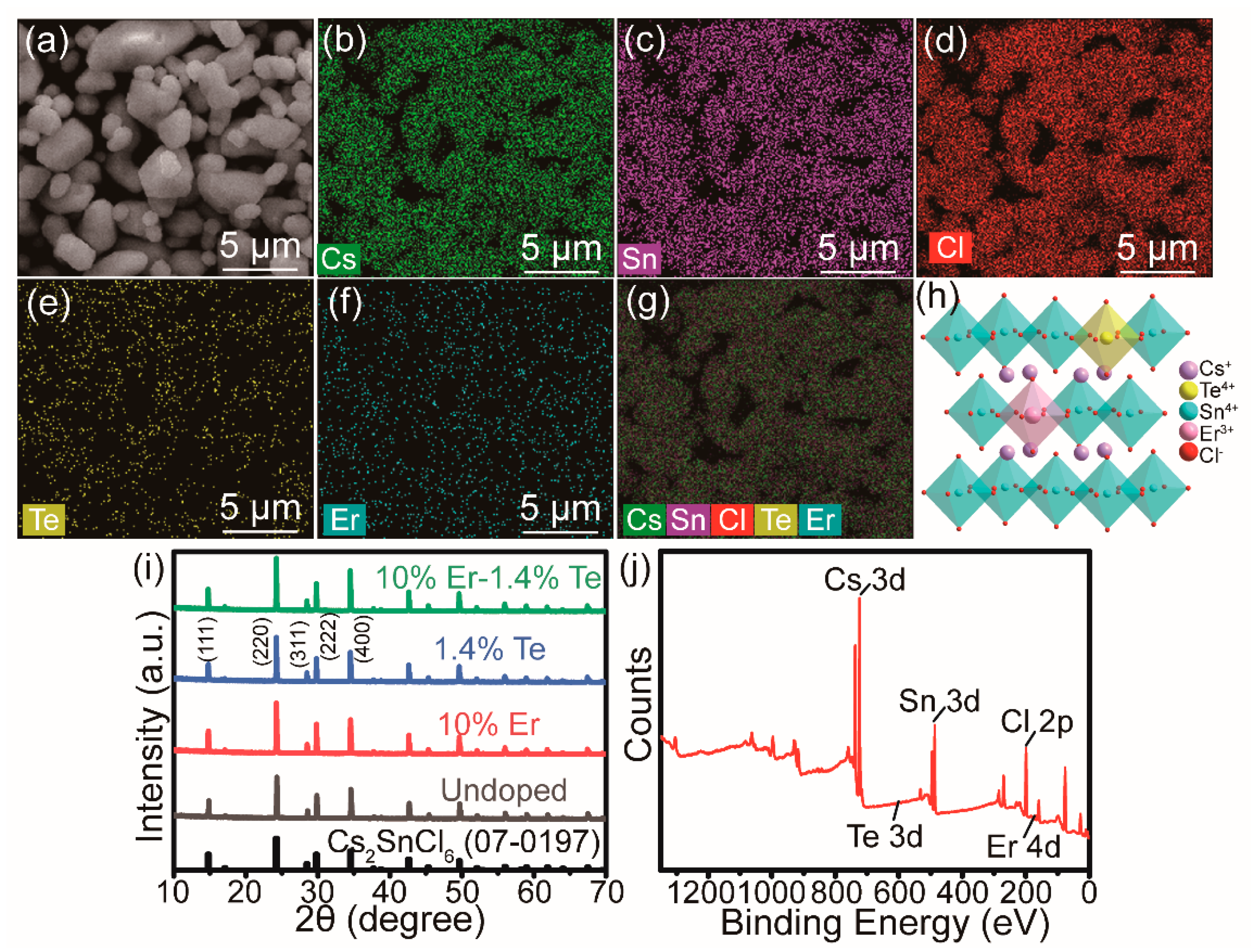
2.1. Crystal Structure and Characterization

The Te4+/Er3+-co-doped Cs2SnCl6 particles were synthesized through a facile co-precipitation method [33]. To be brief, the precursors SnCl4, TeO2, and ErCl3·6H2O were mixed with HCl and ethanol and dissolved. Thereafter, Cs2CO3 (dissolved in HCl) was added into the reaction mixture, and the perovskite MCs were immediately precipitated. More synthesis details are described in the Supporting Information (SI). As depicted in Figure 1a, the scanning electron microscopy (SEM) image showed that the size of the obtained Cs2SnCl6 crystals with a nominal molar concentration of 1.4% Te4+ and 10% Er3+ was mainly in the range of about 1–3 μm (Figure S1). The energy-dispersive spectroscopy (EDS) mapping in Figure 1b–g demonstrated that the constituent elements were uniformly distributed in the microcrystals, and the estimated Cs:(Sn+Te+Er):Cl composition ratio of microcrystals roughly agreed with the stoichiometric ratio of Cs2SnCl6, as given in Table S1. Moreover, the exact doping contents of Te4+ and Er3+ were determined to be 1.6% and 2.0% by inductively coupled plasma mass spectrometry (ICP-MS) (Table S2). It is noted that the Te4+ actual concentration was a little higher than its feeding concentration of 1.4%, which is mainly due to the high solubility of Te4+ in Cs2SnCl6 and the lower formation energy of Cs2TeCl6 than that of Cs2SnCl6 [34,35].
The XRD pattern in Figure 1h,i confirmed the cubic perovskite-type structure of Cs2SnCl6 with space group Fm-3m (PDF no. 07-0197), and no impurity phases were detected. In addition, the Rietveld analysis indicates that the diffraction peaks shifted to lower angles after doping (Figure S2) due to the lattice expansion (Table S3), as Sn4+ (r = 0.69 Å, CN = 6) was substituted by larger Te4+ (r = 0.97 Å, CN = 6) and Er3+ (r = 0.89 Å, CN = 6). These results indicated that Te4+, Er3+, and Te4+/Er3+ were successfully doped into the Cs2SnCl6 crystal lattice. X-ray photoelectron spectroscopy (XPS) was used to analyze the chemical valence state of elements in Cs2SnCl6 crystals (Figure 1j). The binding energies of the Cs 3d (Cs 3d5/2: 723.55 eV, Cs 3d3/2: 737.39 eV), Sn 3d (Sn 3d3/2: 495.74 eV, Sn 3d5/2: 487.24 eV), and Cl 2p (199.06 eV) peaks are consistent with the reported values [36] (Figure S3), proving that the as-prepared Cs2SnCl6 crystals are composed of tetravalent Sn. The peaks located at 586.64 eV and 576.38 eV correspond to Te4+ 3d, and 170.29 eV to Er3+ 4d, respectively. The binding energy of Sn 3d was almost same in un-doped and Te4+-doped samples, while it shifted toward a high energy side in the Te4+/Er3+-co-doped Cs2SnCl6 (Figure S4). After combining the above ICP-MS results, substitutional site of Sn rather than the interstitial site is likely occupied by Te in the doped sample [37].

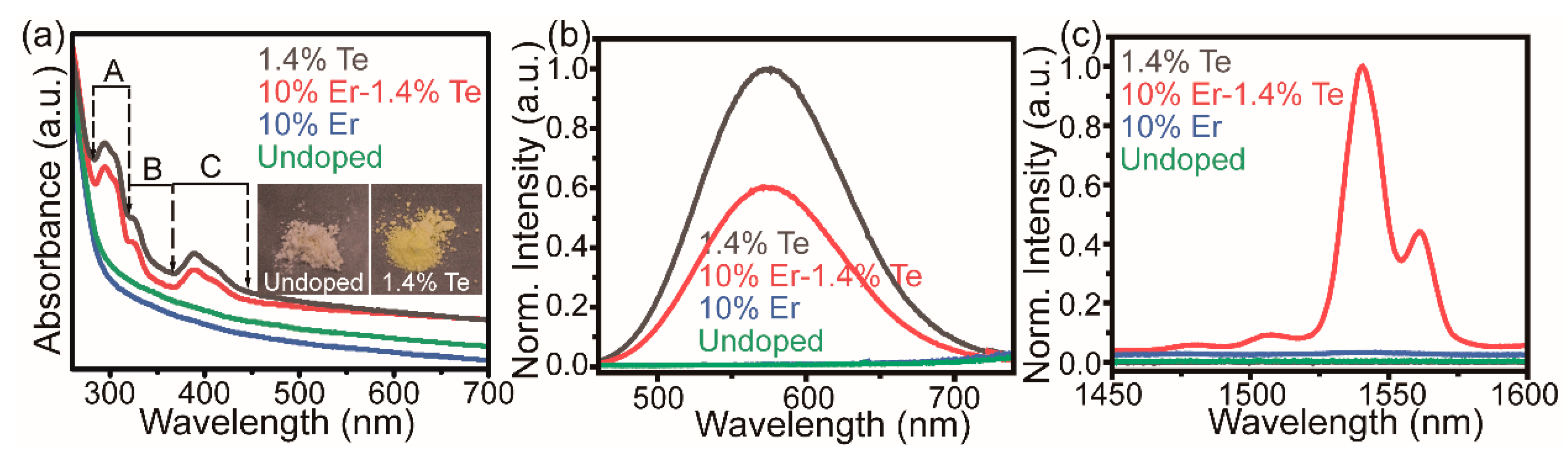
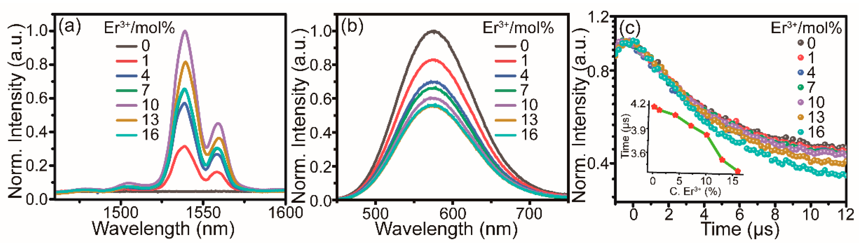
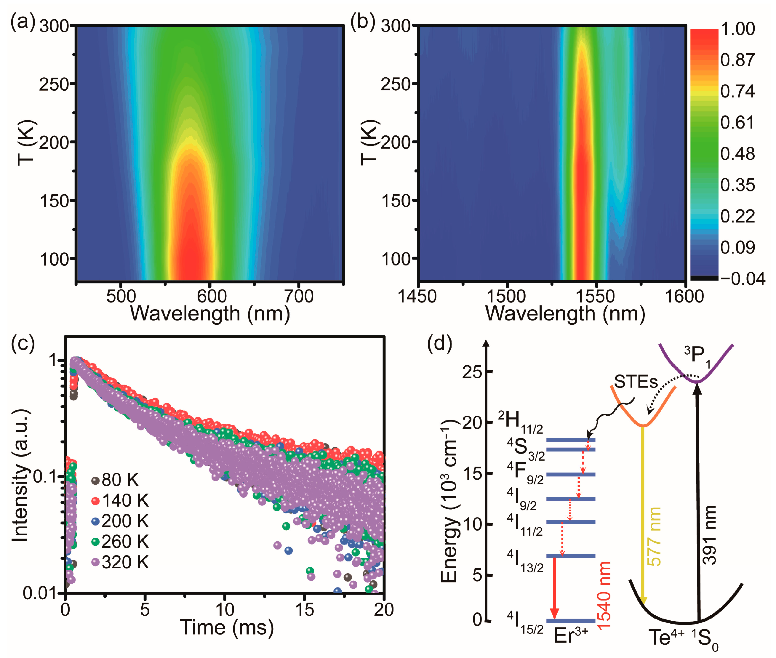
2.2. Optical Properties

The optical properties of Te4+/Er3+-co-doped Cs2SnCl6 microcrystals were investigated via UV–Vis absorption and photoluminescence (PL) spectra. As shown in Figure 2a, Cs2SnCl6 microcrystals showed an optical absorption edge at around 315 nm, which is in agreement with the previous report [22]. While Er3+-singly doped Cs2SnCl6 has a similar result to the undoped one, interestingly, Te4+-singly doped and Te4+/Er3+-co-doped Cs2SnCl6 exhibited intense absorption peaks within the region of 280–450 nm. Compared to the pure white color of the sample without Te4+, these new absorption bands changed the hue of the Te4+-doped Cs2SnCl6 to a luminous yellow (see the photographs in the inset of Figure 2a). In accordance with the absorption spectra, the PL excitation (PLE) spectra also showed peaks between 280 and 450 nm (Figure S5). Thereby, the absorption peaks located at 280–320 nm (A), 320–360 nm (B), and 360–450 nm (C) were derived from the Te4+-induced ion absorption and could be assigned to the inter-configurational 5s2→5s5p transitions of Te4+ [36,38].
The PL spectra of undoped and doped Cs2SnCl6 upon excitation at 391 nm were given in Figure 2b,c. In the visible region, no emission peaks were observed for both the pristine and Er3+-doped Cs2SnCl6 microcrystals (Figure 2b). In contrast, an intense yellow emission at about 577 nm with a large Stokes shift of 127 nm occurs after the doping of Te4+ in Cs2SnCl6, and the luminescence intensity of Te4+/Er3+-co-doped Cs2SnCl6 is a little lower than that of the Te4+-singly doped one. Meanwhile, no emission was observed in the undoped and Te4+-doped Cs2SnCl6 in the NIR region (Figure 2c). Quite weak NIR emissions of Er3+-doped Cs2SnCl6 were observed in the spectra region from 1450 to 1600 nm, originating from the characteristic 4I13/24I15/2 transition of the Er3+ ion (Figure S6) [38,39]. The NIR emission intensity of Er3+-doped Cs2SnCl6 is too weak to evaluate the PLQY. In sharp contrast, Te4+/Er3+-co-doped Cs2SnCl6 displayed an intense NIR emission at 1540 nm and its PLQY was 0.8%. It is also noted that the PL spectrum has other peaks at 1562 nm along with shoulders at around 1480 nm and 1506 nm, which may be caused by the crystal field split manifold of 4I13/2 and 4I15/2 states [40]. The phenomenon that the decreased peak intensity at 577 nm accompanies the enhanced emission at 1540 nm in Te4+/Er3+-co-doped Cs2SnCl6 as compared with the Te4+singly doped sample suggests that the energy transfer and sensitization take place between the luminescent centers Te4+ and Er3+ in the former.
To achieve the highest NIR emission intensity for Te4+/Er3+-co-doped Cs2SnCl6, the Er3+ doping concentration was first optimized to 10% via monitoring the NIR emission intensity of Er3+-doped Cs2SnCl6 (Figure S7). Subsequently, the Te4+ precursor concentrations were varied while keeping a constant Er3+ concentration of 10%. It was seen in Figure S8 that the NIR emission intensity gradually increased to a maximum value at 1.4% Te4+ content and then decreased upon increasing the Te4+ doping amount (0.2–2.6%). The decrease in PL intensity is due to the concentration quenching effect arising from the energy migration among the ions [39]. As discerned in Figure 2c, Te4+-doped Cs2SnCl6 showed no luminescence at all in the NIR region of 1450–1600 nm. However, the luminescence intensity of Er3+ was remarkably enhanced with increasing Te4+ concentrations below 1.4%, which confirms the sensitization effect of Te4+ on the NIR luminescence of Er3+.
To better understand the sensitization effect of Te4+ on the Er3+ NIR emission, PL and time-resolved PL (TRPL) measurements of Te4+/Er3+-co-doped Cs2SnCl6 were carried out at different Er3+ concentrations. As expected, the NIR emission intensity gradually increased with an increasing Er3+ concentration from 0 to 10% (Figure 3a), while the visible PL intensity continuously decreased (Figure 3b). The intensity of NIR emissions declines as the Er3+ concentration exceeds 10%, which suggests the occurrence of the concentration quenching effect. For Er3+-singly doped Cs2SnCl6, however, different Er3+ doping amounts all lead to a negligible NIR luminescence (Figure S9). At the same time, the visible luminescence lifetimes of Te4+/Er3+-co-doped Cs2SnCl6 also decreased from 4.18 to 3.39 with the increase in the Er3+ concentration (Figure 3c, Table S4), which corresponds to the continuously increasing energy transfer efficiency (1 − τx0, where τ0 is the lifetime of visible luminescence with Er3+ doping amount x = 0 [41].) of Te4+/Er3+ from 0.96% to 18.9% and benefits intense NIR emissions.
Furthermore, temperature-dependent PL spectra were studied for the as-prepared Te4+/Er3+-co-doped Cs2SnCl6. Figure 4a showed that the PL intensities of Te4+ declined monotonically upon increasing the temperature from 80 K to 300 K. This is attributed to the increased non-radiative transition probability of Te4+ at higher temperatures and the thermal-enhanced energy transfer from Te4+ to Er3+ [33]. In addition, the full width at half maximum (FWHM) increased as the temperature increased (Figure S10). A high Huang–Rhys factor (S) of 18 was obtained according to the temperature dependence of FWHM, which reveals the strong electron–phonon coupling effect in Cs2SnCl6:Te and facilitates the formation of STEs [24]. Nevertheless, the integrated PL intensities of Er3+ increased slightly with rising temperature (Figure 4b and Figure S11), which was accompanied by small variations in the PL lifetime at 1540 nm within this temperature range (Figure 4c, Table S5). The temperature-stable PL intensity of the NIR emission reflected a good protection of Er3+ 4f electrons by the outer electrons in 5s25p6 shells [42]. It is worth noting that the intensity ratio of I1540/I1562 declined with an increasing temperature (Figure S12). This variation is caused by the population redistribution among crystal field split manifolds of 4I13/2 and 4I15/2 states at different temperatures, which is consistent with the similar observations made in different Er3+-doped hosts [39,43].
According to the above optical results, the energy transfer mechanism was described in Figure 4d based on the energy level alignment of Te4+ and Er3+. Thanks to the strong electron-phonon coupling in Cs2SnCl6 with soft lattice, transient elastic lattice deformation occurs upon photogeneration, where excitons tend to be self-trapped due to its lower energy and form self-trapped excitons (STEs) [43]. Therefore, carriers excited from 1S0 to 3P1 of Te4+ ion under 391 nm excitation relax to form STEs, which then recombine to yield the broad band yellow emission at 577 nm in Te4+ doped Cs2SnCl6. For Er3+ singly-doped samples, the electrons in ground state 4I15/2 transited to excited state 4I13/2 under low energy excitation, and then generated very weak NIR emission (1540 nm) due to the parity-forbidden transitions within the 4fN configurations [24,40]. In Te4+/Er3+ co-doped Cs2SnCl6, however, partial excitation energy was transferred from STEs to the well-matched 2H11/2 energy level of Er3+ ions in addition to the yellow emission [33,37]. The transferred carriers relaxed non-radiatively to the 4I13/2 energy level, and finally return to the ground states of the 4I15/2 energy level through radiative transition, resulting in the enhanced 1540 nm NIR emissions at the expense of the weakened yellow luminescence from STEs.

2.3. Moisture Stability

Moisture stability is essential for practical applications of perovskite materials. Impressively, the NIR emission was very stable when the samples were exposed to air and even immersed in water. As shown in Figure S13, the XRD pattern of Te4+/Er3+-co-doped Cs2SnCl6 microcrystals was basically unchanged after being left in ambient air for 100 days. The PL intensity decreased by only 13% compared to the original data (Figure S14). Moreover, a strong NIR emission of the microcrystals was maintained after being immersed in deionized water for 2 h (Figure S15). Even after the samples were soaked in water for 8 h, the emissions still remained at 30% of the initial level, while the shape and position of XRD peaks remained unchanged (Figure S16). The superior stability in both the structure and NIR luminescence renders Cs2SnCl6 microcrystals more promising for practical applications relative to the common lead halide perovskites.

3. Conclusions

In conclusion, intense and multiple NIR emissions at 1540 nm and 1562 nm were achieved in a Sn-based double perovskite Cs2SnCl6 through Te4+/Er3+ co-doping. Under a low energy excitation at 391 nm, the NIR luminescence originating from the 4f→4f transition of Er3+ was significantly enhanced due to the effective energy transfer from the 1S03P1 transition of Te4+. Furthermore, the Te4+/Er3+ Cs2SnCl6 microcrystals prepared via the simple co-precipitation method exhibited excellent emission and moisture stability. These findings bring novel emissive features to Cs2SnCl6 double perovskites, thus expanding their optoelectronic properties for future applications, such as NIR biosensors, anti-counterfeit technologies, and optical fiber communication.

Supplementary Materials

The following supporting information can be downloaded at: https://www.mdpi.com/article/10.3390/molecules28083593/s1, Figure S1: Particle size statistics of MCs; Figure S2: Enlarged shifts of (220) peak of MCs; Figure S3: XPS spectra of MCs; Figure S4: Representative XPS spectra of Sn 3d in the MCs; Figure S5: PLE spectra of MCs in the visible region; Figure S6: PL spectra of MCs in the NIR region; Figure S7: PL emission spectra of MCs in the NIR region; Figure S8: PL emission spectra of x% Te4+-10% Er3+ co-doped MCs; Figure S9: NIR intensity variations of MCs with different Er3+ concentrations; Figure S10: Fitting results of the FWHM; Figure S11: Integral intensity of NIR peak at different temperatures ; Figure S12: Peak intensity ratio of 1540 nm (I1540)/1562 nm (I1562) emissions at different temperatures; Figure S13: XRD patterns of MCs before and after their exposure to ambient air; Figure S14: PL emission spectra of MCs before and after their exposure to ambient air; Figure S15: PL emission spectra of MCs before and after their soak in water; Figure S16: XRD patterns of MCs before and after their soak in water; Table S1: Elemental analyses of the MCs by EDS; Table S2: Results of the Te and Er ion ICP-MS test in MCs; Table S3: The calculated lattice parameters of MCs via XRD peaks; Table S4: Average PL lifetimes of MCs with different Er3+ concentrations; Table S5: Temperature-dependent PL lifetimes of MCs.

Author Contributions

X.Q.: formal analysis, investigation, validation and data curation; C.W.: conceptualization, supervision and writing—original draft preparation; X.H.: conceptualization, supervision, funding acquisition and writing—review and editing. All authors have read and agreed to the published version of the manuscript.

Funding

This work was supported by the National Natural Science Foundation of China (Grant No. 62064005), the Double Thousand Plan of Jiangxi Province (Grant No. jxsq2018101019), the Technology Research Project of Jiangxi Provincial Department of Education (Grant No. GJJ210871), the Scientific Research Foundation of Jiangxi University of Science and Technology (Grant No. 205200100565, 205200100100), and the Innovative Talents Program of Ganzhou (Grant No. 2022CXRC9294).

Institutional Review Board Statement

Not applicable.

Informed Consent Statement

Not applicable.

Data Availability Statement

Not applicable.

Conflicts of Interest

The authors declare no competing financial interests.

Sample Availability

Samples of the compounds are not available from the authors.

References

  1. Castriotta, L.A.; Calabrò, E.; Di Giacomo, F.; Reddy, S.H.; Takhellambam, D.; Paci, B.; Generosi, A.; Serenelli, L.; Menchini, F.; Martini, L.; et al. A universal multi-additive strategy to enhance efficiency and stability in inverted perovskite solar cells. Nano Energy 2023, 109, 108268. [Google Scholar] [CrossRef]
  2. Wu, X.; Yin, C.; Zhang, M.; Xie, Y.; Hu, J.; Long, R.; Wu, X.; Wu, X. The intercalation cathode of MOFs-driven vanadium-based composite embedded in n-doped carbon for aqueous zinc ion batteries. Chem. Eng. J. 2023, 452, 139573. [Google Scholar] [CrossRef]
  3. Zhang, Y.; Kim, S.G.; Lee, D.; Shin, H.; Park, N.G. Bifacial stamping for high efficiency perovskite solar cells. Energ. Environ. Sci. 2019, 12, 308–321. [Google Scholar] [CrossRef]
  4. Li, X.; Wu, Y.; Zhang, S.; Cai, B.; Gu, Y.; Song, J.; Zeng, H. CsPbX3 quantum dots for lighting and displays: Room-temperature synthesis, photoluminescence superiorities, underlying origins and white light-emitting diodes. Adv. Funct. Mater. 2016, 26, 2435–2445. [Google Scholar] [CrossRef]
  5. Liu, H.; Wu, Z.; Gao, H.; Shao, J.; Zou, H.; Yao, D.; Liu, Y.; Zhang, H.; Yang, B. One-step preparation of cesium lead halide CsPbX3 (X = Cl, Br, and I) perovskite nanocrystals by microwave irradiation. ACS Appl. Mater. Interfaces 2017, 9, 42919–42927. [Google Scholar] [CrossRef]
  6. Yu, Y.L.; Yang, W.Y.; Hara, A.; Asayama, K.; Roles, H.; Nawrot, T.; Staessen, J. Public and occupational health risks related to lead exposure updated according to present-day blood lead levels. Hypertens. Res. 2022, 46, 395–407. [Google Scholar] [CrossRef]
  7. Olufemi, A.C.; Mji, A.; Mukhola, M.S. Potential health risks of lead exposure from early life through later life: Implications for public health education. Int. J. Environ. Res. Public Health 2022, 19, 16006. [Google Scholar] [CrossRef] [PubMed]
  8. Jellicoe, T.C.; Richter, J.M.; Glass, H.F.J.; Tabachnyk, M.; Brady, R.; Dutt, S.E.; Rao, A.; Friend, R.H.; Credgington, D.; Greenham, N.C.; et al. Synthesis and optical properties of lead-free cesium tin halide perovskite nanocrystals. J. Am. Chem. Soc. 2016, 138, 2941–2944. [Google Scholar] [CrossRef]
  9. Men, L.; Rosales, B.A.; Gentry, N.E.; Cady, S.D.; Vela, J. Lead-free semiconductors: Soft chemistry, dimensionality control, and manganese-doping of germanium halide perovskites. ChemNanoMat 2019, 5, 334–339. [Google Scholar] [CrossRef]
  10. Ghosh, B.; Wu, B.; Mulmudi, H.K.; Guet, C.; Weber, K.; Sum, T.C.; Mhaisalkar, S.; Mathews, N. Limitations of Cs3Bi2I9 as lead-free photovoltaic absorber materials. ACS Appl. Mater. Interfaces 2018, 10, 35000–35007. [Google Scholar] [CrossRef]
  11. Han, P.; Zhou, W.; Zheng, D.; Zhang, X.; Li, C.; Kong, Q.; Yang, S.; Lu, R.; Han, K. Lead-free all-inorganic indium chloride perovskite variant nanocrystals for efficient luminescence. Adv. Opt. Mater. 2022, 10, 2101344. [Google Scholar] [CrossRef]
  12. Li, D.; Xu, W.; Zhou, D.; Ma, X.; Chen, X.; Pan, G.; Zhu, J.; Ji, Y.; Ding, N.; Song, H.; et al. Cesium tin halide perovskite quantum dots as an organic photoluminescence probe for lead ion. J. Lumin. 2019, 216, 116711. [Google Scholar] [CrossRef]
  13. Liu, Q.; Yin, J.; Zhang, B.B.; Chen, J.K.; Zhou, Y.; Zhang, L.M.; Wang, L.M.; Zhao, Q.; Hou, J.; Shu, J.; et al. Theory-guided synthesis of highly luminescent colloidal cesium tin halide perovskite nanocrystals. J. Am. Chem. Soc. 2021, 143, 5470–5480. [Google Scholar] [CrossRef] [PubMed]
  14. Kang, C.; Rao, H.; Fang, Y.; Zeng, J.; Pan, Z.; Zhong, X. Antioxidative stannous oxalate derived lead-free stable CsSnX3 (X = Cl, Br, and I) perovskite nanocrystals. Angew. Chem. Int. Ed. 2021, 133, 670–675. [Google Scholar] [CrossRef]
  15. Chu, Y.; Hu, Y.; Xiao, Z. First-principles insights into the stability difference between ABX3 halide perovskites and their A2BX6 variants. J. Phys. Chem. C 2021, 125, 9688–9694. [Google Scholar] [CrossRef]
  16. Liu, F.; Jiang, J.; Toyoda, T.; Kamarudin, M.A.; Hayase, S.; Wang, R.; Tao, S.; Shen, Q. Ultra-halide-rich synthesis of stable pure tin-based halide perovskite quantum dots: Implications for photovoltaics. ACS Appl. Nano Mater. 2021, 4, 3958–3968. [Google Scholar] [CrossRef]
  17. Zhang, X.; Wu, X.; Liu, X.; Chen, G.; Wang, Y.; Bao, J.; Xu, X.; Liu, X.; Zhang, Q.; Yu, K.; et al. Heterostructural CsPbX3-PbS (X= Cl, Br, I) quantum dots with tunable Vis-NIR dual emission. J. Am. Chem. Soc. 2020, 142, 4464–4471. [Google Scholar] [CrossRef]
  18. Zeng, M.; Locardi, F.; Mara, D.; Hens, Z.; Deun, R.; Artizzu, F. Switching on near-infrared light in lanthanide-doped CsPbCl3 perovskite nanocrystals. Nanoscale 2021, 13, 8118–8125. [Google Scholar] [CrossRef]
  19. Yin, Y.; Huang, Y.; Wu, Y.; Chen, G.; Yin, W.J.; Wei, S.H.; Gong, X. Exploring emerging photovoltaic materials beyond perovskite: The case of skutterudite. Chem. Mater. 2017, 29, 9429–9435. [Google Scholar] [CrossRef]
  20. Kovalenko, M.V.; Protesescu, L.; Bodnarchuk, M.I. Properties and potential optoelectronic applications of lead halide perovskite nanocrystals. Science 2017, 358, 745–750. [Google Scholar] [CrossRef]
  21. Arfin, H.; Kshirsagar, A.S.; Kaur, J.; Mondal, B.; Xia, Z.; Chakraborty, S.; Nag, A. ns2 electron (Bi3+ and Sb3+) doping in lead-free metal halide perovskite derivatives. Chem. Mater. 2020, 32, 10255–10267. [Google Scholar] [CrossRef]
  22. Tan, Z.; Li, J.; Zhang, C.; Li, Z.; Hu, Q.; Xiao, Z.; Kamiya, T.; Hosono, H.; Niu, G.; Lifshitz, E.; et al. Highly efficient blue-emitting Bi-doped Cs2SnCl6 perovskite variant: Photoluminescence induced by impurity doping. Adv. Funct. Mater. 2018, 28, 1801131. [Google Scholar] [CrossRef]
  23. Jing, Y.; Liu, Y.; Zhao, J.; Xia, Z. Sb3+ doping-induced triplet self-trapped excitons emission in lead-free Cs2SnCl6 nanocrystals. J. Phys. Chem. Lett. 2019, 10, 7439–7444. [Google Scholar] [CrossRef]
  24. Tan, Z.; Chu, Y.; Chen, J.; Li, J.; Ji, G.; Niu, G.; Gao, L.; Xiao, Z.; Tang, J. Lead-free perovskite variant solid solutions Cs2Sn1–xTexCl6: Bright luminescence and high anti-water stability. Adv. Mater. 2020, 32, 2002443. [Google Scholar] [CrossRef]
  25. Adhikari, S.D.; Echeverría-Arrondo, C.; Sánchez, R.S.; Chirvony, V.S.; Martínez-Pastor, J.P.; Agouram, S.; Muñoz-Sanjosé, V.; Mora-Seró, L. White light emission from lead-free mixed-cation doped Cs2SnCl6 nanocrystals. Nanoscale 2022, 14, 1468–1479. [Google Scholar] [CrossRef] [PubMed]
  26. Zhong, Y.; Huang, Y.E.; Deng, T.; Lin, Y.T.; Huang, X.Y.; Deng, Z.H.; Du, K.Z. Multi-dopant engineering in perovskite Cs2SnCl6: White light emitter and spatially luminescent heterostructure. Inorg. Chem. 2021, 60, 17357–17363. [Google Scholar] [CrossRef] [PubMed]
  27. Hwang, A.; Park, M.; Park, Y.; Shim, Y.; Youn, S.; Lee, C.-H.; Jeong, H.B.; Jeong, H.Y.; Chang, J.; Lee, K.; et al. Visible and infrared dual-band imaging via Ge/MoS2 van der Waals heterostructure. Sci. Adv. 2021, 7, eabj2521. [Google Scholar] [CrossRef]
  28. Pan, Q.; Cai, Z.; Yang, Y.; Yang, D.; Kang, S.; Chen, Z.; Qiu, J.; Zhan, Q.; Dong, G. Engineering tunable broadband near-infrared emission in transparent rare-earth doped nanocrystals-in-glass composites via a bottom-up strategy. Adv. Opt. Mater. 2019, 7, 1801482. [Google Scholar] [CrossRef]
  29. Wu, W.; Zhang, X.; Kornienko, A.Y.; Kumar, G.A.; Yu, D.; Emge, T.J.; Riman, R.E.; Brennan, J.G. Efficient NIR emission from Nd, Er, and Tm complexes with fluorinated selenolate ligands. Inorg. Chem. 2018, 57, 1912–1918. [Google Scholar] [CrossRef]
  30. Mukthar, N.F.M.; Schley, N.D.; Ung, G. Strong circularly polarized luminescence at 1550 nm from enantiopure molecular erbium complexes. J. Am. Chem. Soc. 2022, 144, 6148–6153. [Google Scholar] [CrossRef]
  31. Cai, T.; Wang, J.; Li, W.; Hills-Kimball, K.; Yang, H.; Nagaoka, Y.; Yuan, Y.; Zia, R.; Chen, O. Mn2+/Yb3+ codoped CsPbCl3 perovskite nanocrystals with triple-wavelength emission for luminescent solar concentrators. Adv. Sci. 2020, 7, 2001317. [Google Scholar] [CrossRef]
  32. Mahor, Y.; Mir, W.J.; Nag, A. Synthesis and near-infrared emission of Yb-doped Cs2AgInCl6 double perovskite microcrystals and nanocrystals. J. Phys. Chem. C 2019, 123, 15787–15793. [Google Scholar] [CrossRef]
  33. Sun, J.; Zheng, W.; Huang, P.; Zhang, M.; Zhang, W.; Deng, Z.; Yu, S.; Jin, M.; Chen, X. Efficient near-infrared luminescence in lanthanide-doped vacancy-ordered double perovskite Cs2ZrCl6 phosphors via Te4+ sensitization. Angew. Chem. Int. Ed. 2022, 61, e202201993. [Google Scholar]
  34. Fedorovskiy, A.E.; Drigo, N.A.; Nazeeruddin, M.K. The role of Goldschmidt’s tolerance factor in the formation of A2BX6 double halide perovskites and its optimal range. Small Methods 2020, 4, 1900426. [Google Scholar] [CrossRef]
  35. Diao, X.; Diao, Y.; Tang, Y.; Zhao, G.; Gu, Q.; Xie, Y.; Shi, Y.; Zhu, P.; Zhang, L. High-throughput screening of stable and efficient double inorganic halide perovskite materials by DFT. Sci. Rep. 2022, 12, 12633. [Google Scholar] [CrossRef]
  36. Zhang, W.; Zheng, W.; Li, L.; Huang, P.; Gong, Z.; Zhou, Z.; Sun, J.; Yu, Y.; Chen, X. Dual-band-tunable white-light emission from Bi3+/Te4+ emitters in perovskite-derivative Cs2SnCl6 microcrystals. Angew. Chem. Int. Ed. 2022, 61, e202116085. [Google Scholar]
  37. Zeng, R.; Bai, K.; Wei, Q.; Chang, T.; Yan, J.; Ke, B.; Huang, J.; Wang, L.; Zhou, W.; Cao, S.; et al. Boosting triplet self-trapped exciton emission in Te (IV)-doped Cs2SnCl6 perovskite variants. Nano Res. 2021, 14, 1551–1558. [Google Scholar] [CrossRef]
  38. Drummen, P.J.H.; Donker, H.; Smit, W.M.A.; Blasse, G. Jahn-Teller distortion in the excited state of tellurium (IV) in Cs2MCl6 (M = Zr, Sn). Chem. Phys. Lett. 1988, 144, 460–462. [Google Scholar] [CrossRef]
  39. Liao, J.; Zhang, P.; Niu, X.; Hong, H.; Yin, H.; Li, Z.; Yin, H.; Chen, Z. Co-doping of stibium and rare earth (Nd, Yb) in lead-free double perovskite for efficient near-infrared emission. J. Alloys Compd. 2022, 911, 164946. [Google Scholar] [CrossRef]
  40. Zhao, J.; Pan, G.; Liu, K.; You, W.; Jin, S.; Zhu, Y.; Gao, H.; Zhang, H.; Mao, Y. Efficient dual-mode emissions of high-concentration erbium ions doped lead-free halide double perovskite single crystals. J. Alloys Compd. 2022, 895, 162601. [Google Scholar] [CrossRef]
  41. Cao, L.; Jia, X.; Gan, W.; Ma, C.G.; Zhang, J.; Lou, B.; Wang, J. Strong self-trapped exciton emission and highly efficient near-infrared luminescence in Sb3+-Yb3+ co-doped Cs2AgInCl6 double perovskite. Adv. Funct. Mater. 2023, 33, 2212135. [Google Scholar] [CrossRef]
  42. Arfin, H.; Kaur, J.; Sheikh, T.; Chakraborty, S.; Nag, A. Bi3+-Er3+ and Bi3+-Yb3+ codoped Cs2AgInCl6 double perovskite near-infrared emitters. Angew. Chem. Int. Ed. 2020, 59, 11307–11311. [Google Scholar] [CrossRef] [PubMed]
  43. Wu, R.; Han, P.; Zheng, D.; Zhang, J.; Yang, S.; Zhao, Y.; Miao, X.; Han, K. All-inorganic rare-earth-based double perovskite nanocrystals with near-infrared emission. Laser Photonics Rev. 2021, 15, 2100218. [Google Scholar] [CrossRef]
Figure 1. (a) SEM image, (bg) EDS elemental mappings (Cs, Sn, Cl, Te, Er, and merge), and (h) crystal structure of cubic Te4+/Er3+-co-doped Cs2SnCl6. (i) XRD pattern of undoped, Er3+-singly doped, Te4+-singly doped, and Te4+/Er3+-co-doped Cs2SnCl6 microcrystals. The 2θ peaks located at 14.8°, 24.2°, 28.5°, 29.7°, and 34.5° correspond to the (111), (220), (311), (222), and (400) diffraction planes, respectively. (j) XPS survey spectrum of Te4+/Er3+-co-doped Cs2SnCl6 microcrystals.
Molecules 28 03593 g001
Figure 2. (a) UV–Vis absorption spectra of undoped, Er3+-doped, Te4+-doped, and Te4+/Er3+-co-doped Cs2SnCl6 microcrystals. The inset shows photographs of undoped and Te4+-doped Cs2SnCl6 microcrystals. Normalized PL spectra (λex = 391 nm) of undoped, Er3+-doped, Te4+-doped and Te4+/Er3+-co-doped Cs2SnCl6 microcrystals (b) in the visible region and (c) in the NIR region.
Molecules 28 03593 g002
Figure 3. Normalized PL emission spectra (λex = 391 nm) of 1.4% Te4+/x% Er3+-co-doped Cs2SnCl6 microcrystals (a) in the NIR region and (b) in the visible region. (c) Visible luminescence decay curves of 1.4% Te4+/x% Er3+-co-doped Cs2SnCl6 (λex = 391 nm and λem = 577 nm). Inset shows the PL lifetime of 1.4% Te4+/x% Er3+-co-doped Cs2SnCl6 for the visible emission as a function of Er3+ concentration.
Molecules 28 03593 g003
Figure 4. Contour plots of the normalized temperature-dependent PL emission spectra of Te4+/Er3+-co-doped Cs2SnCl6 microcrystals under excitation at 391 nm (a) in the visible region and (b) in the NIR region. (c) PL decay curves of 1540 nm emission measured at different temperatures in Te4+/Er3+-co-doped Cs2SnCl6 microcrystals (λex = 391 nm). (d) Schematic illustration of luminescence mechanisms in Te4+/Er3+-co-doped Cs2SnCl6 microcrystals. The full, dashed, and curve arrows represent the radiative transition, non-radiative transition, and energy transfer process, respectively.
Molecules 28 03593 g004
Disclaimer/Publisher’s Note: The statements, opinions and data contained in all publications are solely those of the individual author(s) and contributor(s) and not of MDPI and/or the editor(s). MDPI and/or the editor(s) disclaim responsibility for any injury to people or property resulting from any ideas, methods, instructions or products referred to in the content.

