Diffusion Barrier Performance of AlCrTaTiZr/AlCrTaTiZr-N High-Entropy Alloy Films for Cu/Si Connect System


Abstract
:1. Introduction
2. Experimental Details
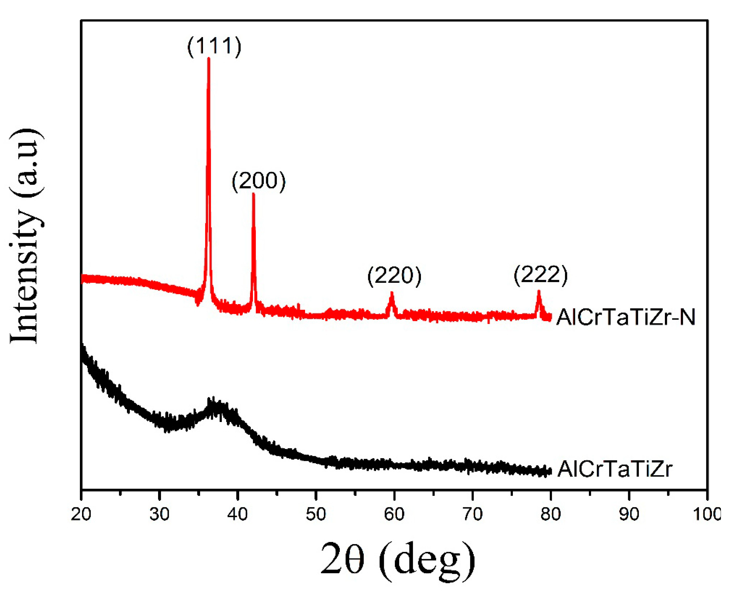
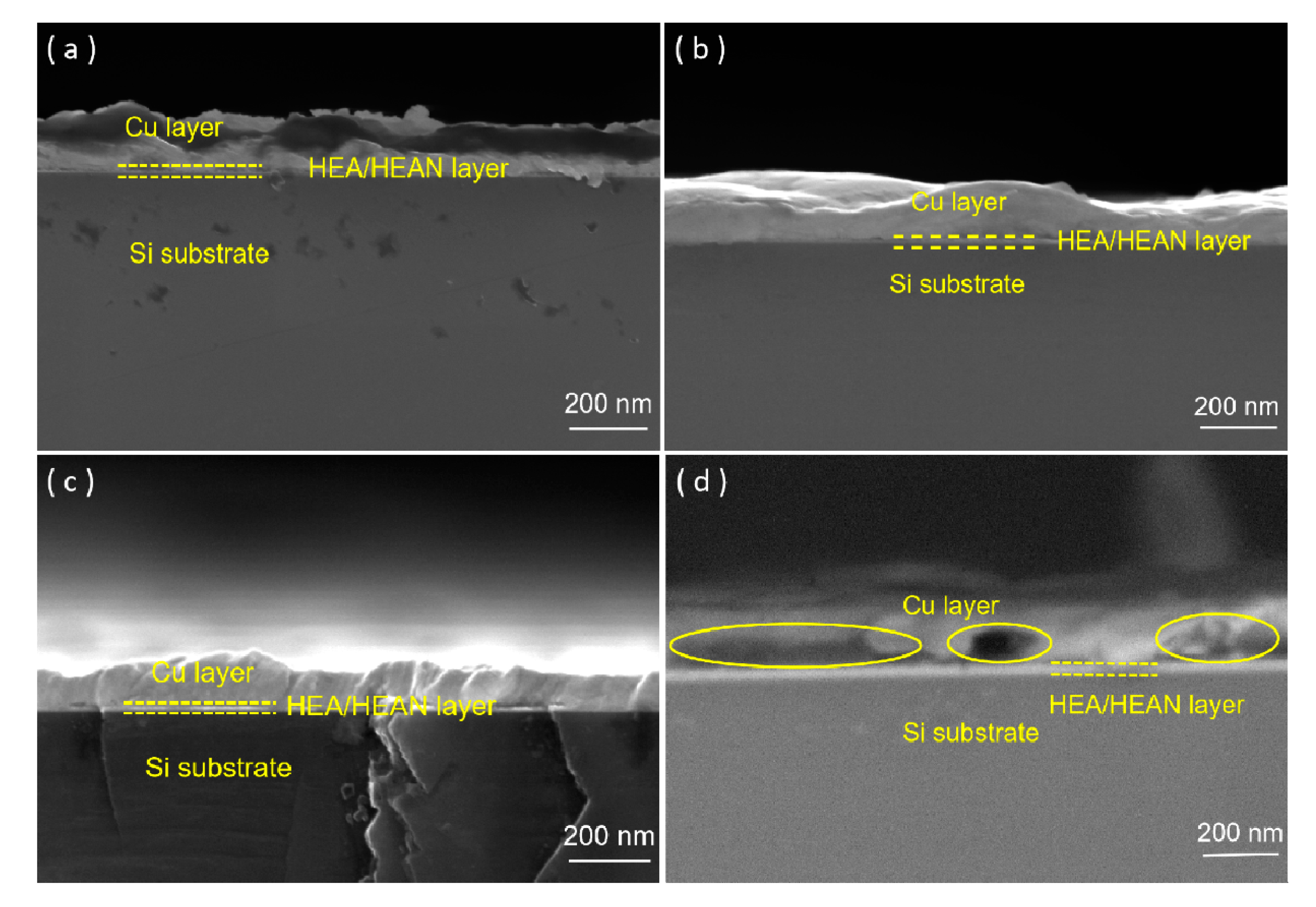
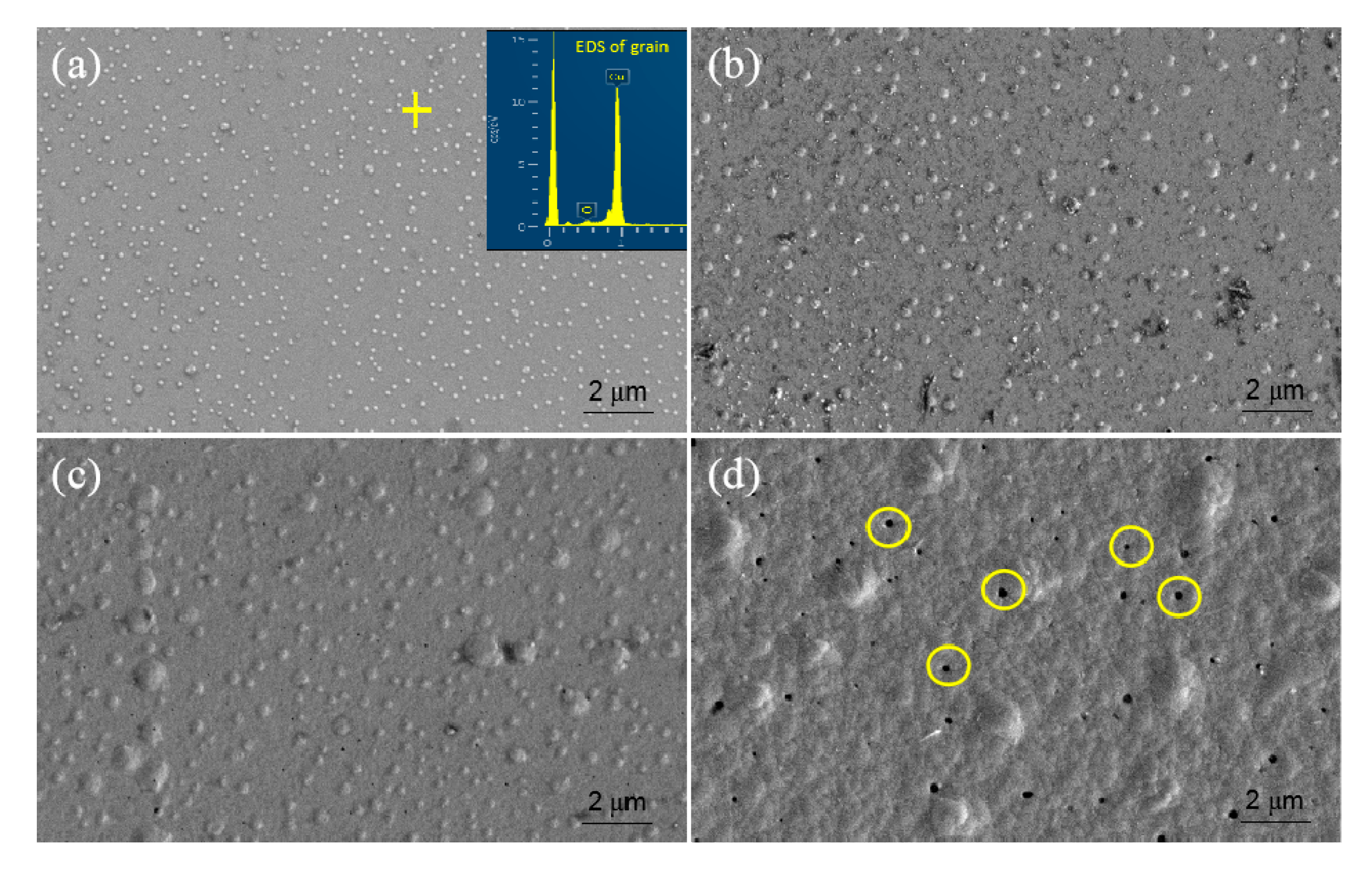
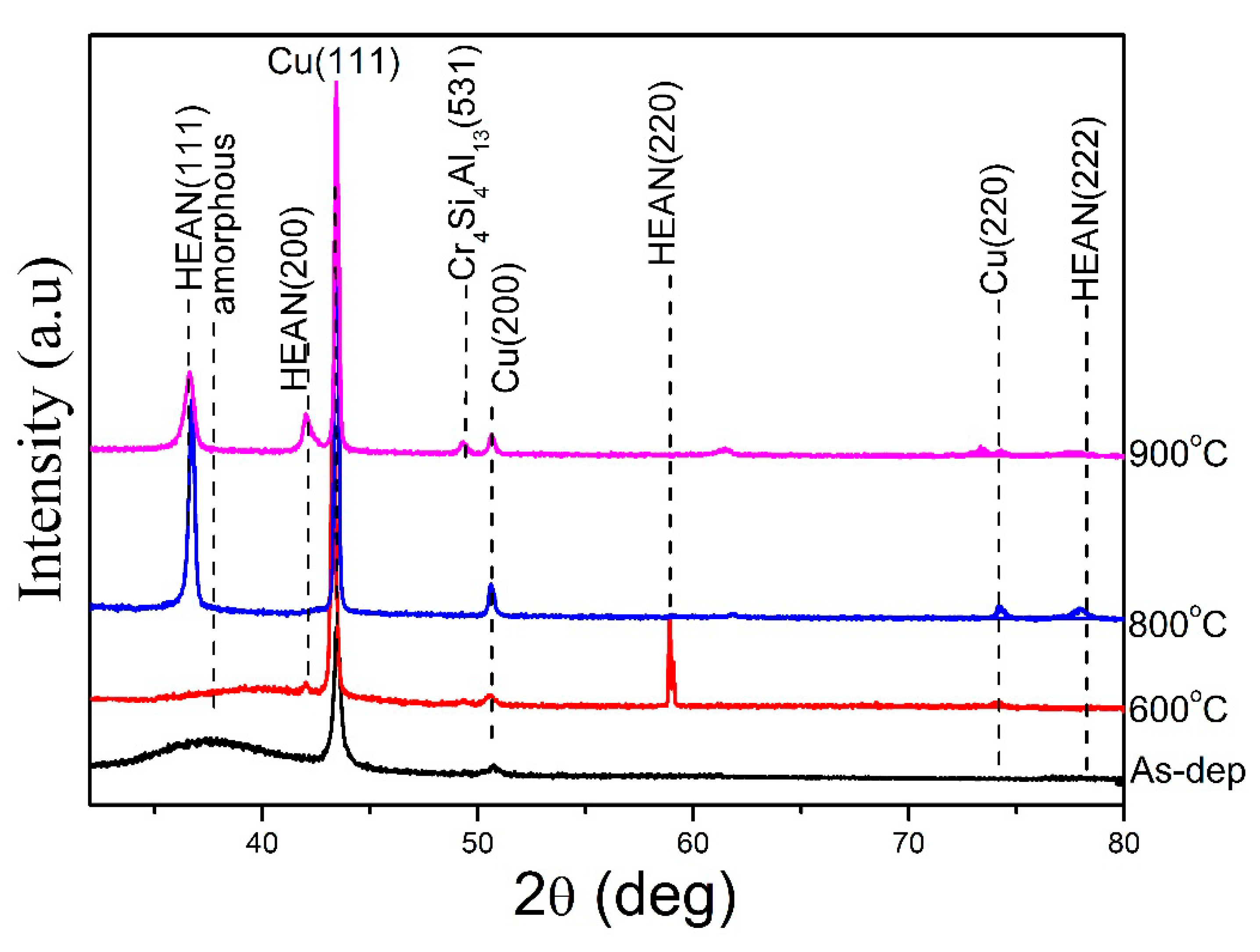
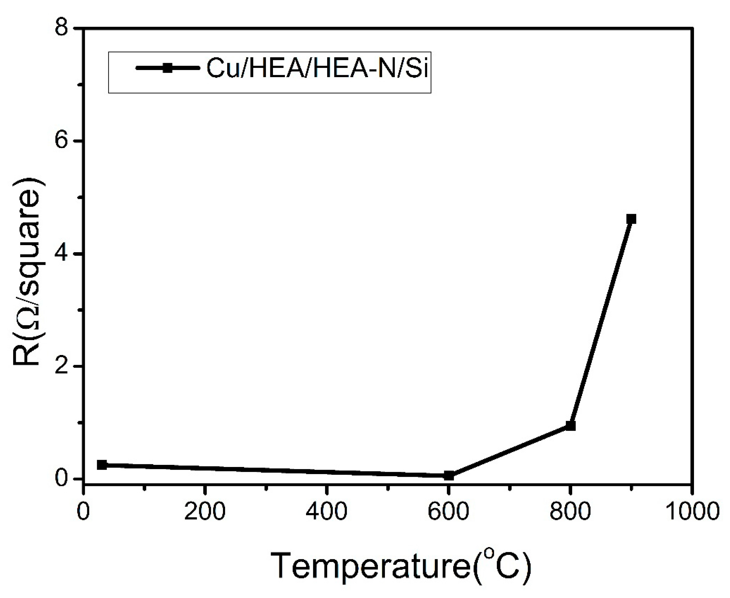
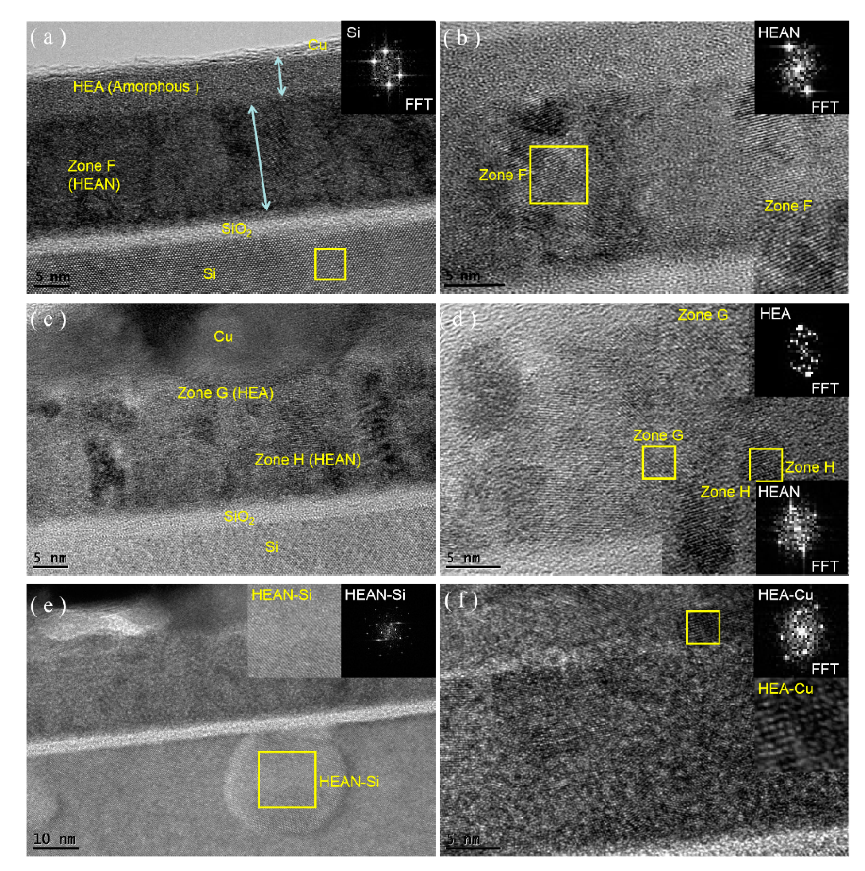
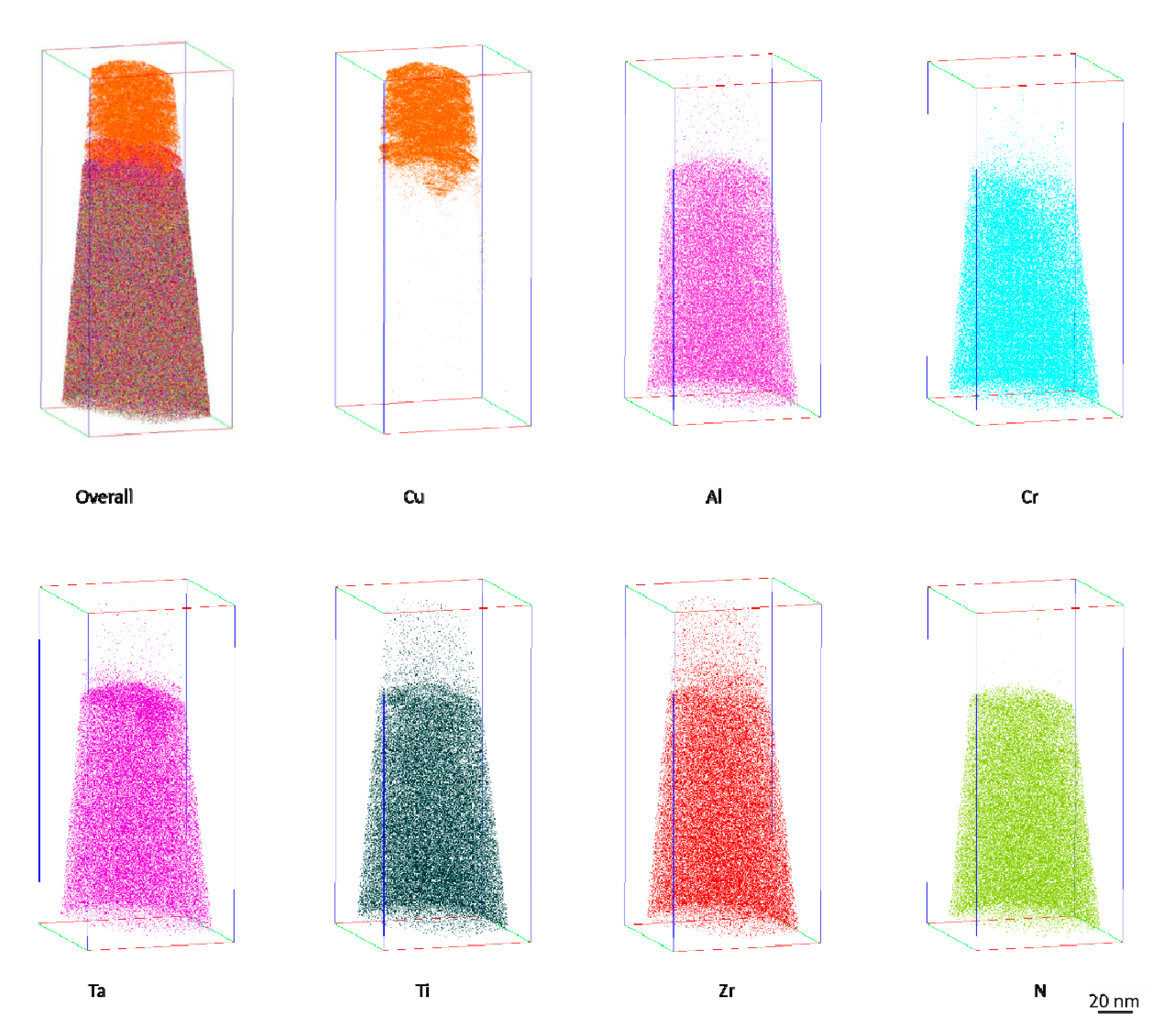
3. Results
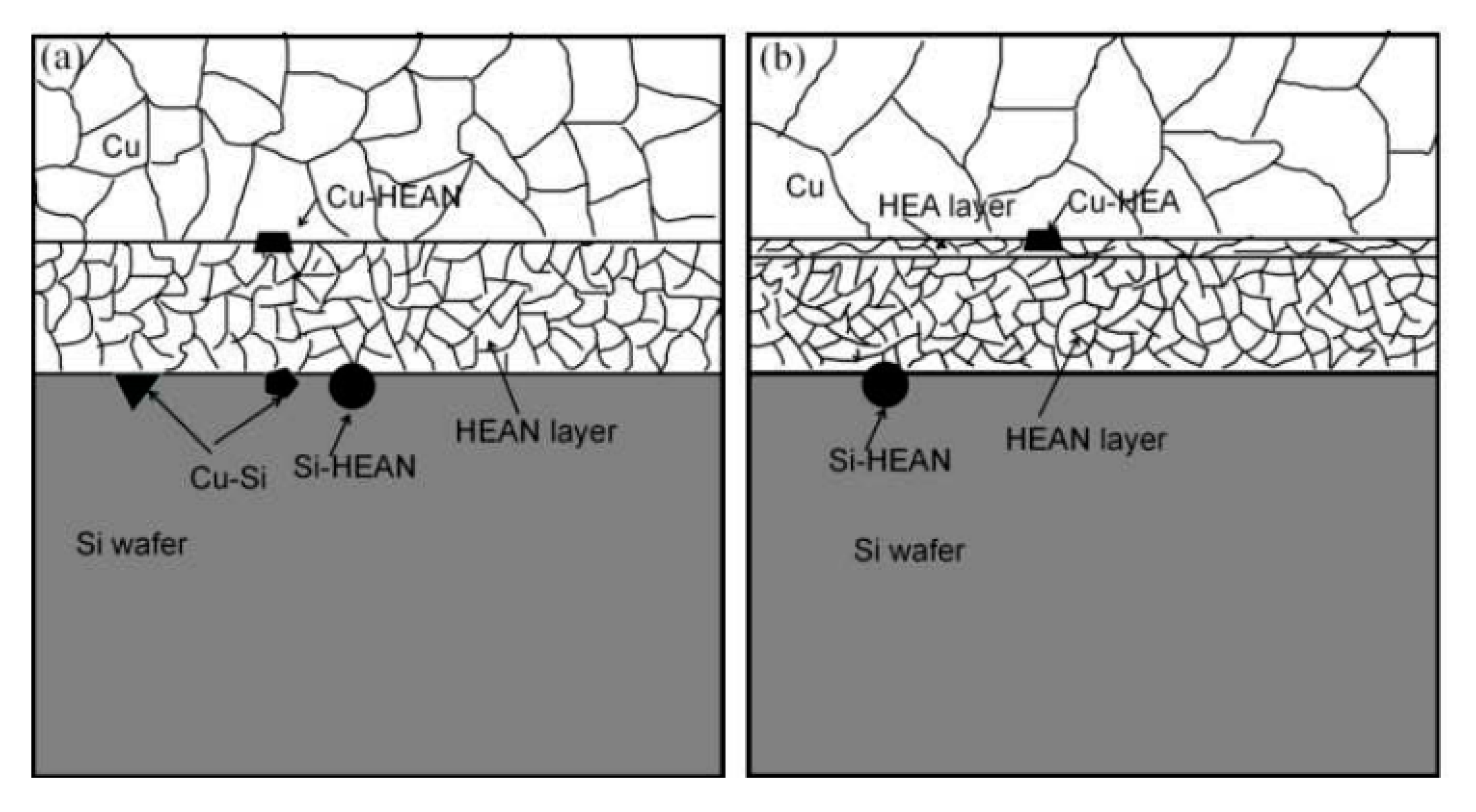
4. Discussion
5. Conclusions
Author Contributions
Funding
Acknowledgments
Conflicts of Interest
References
- Nitta, T.; Ohmi, T.; Otsuki, M.; Takewaki, T.; Shibata, T. Electrical properties of giant-grain copper thin films formed by a low kinetic energy particle process. J. Electrochem Soc. 1992, 139, 922–927. [Google Scholar] [CrossRef]
- Chang, C.-A. Outdiffusion of Cu through Au: Comparison of (100) and (111) Cu films epitaxially deposited on Si, and effects of annealing ambients. Appl. Phys. Lett. 1989, 55, 2754–2756. [Google Scholar] [CrossRef]
- Takeyama, M.B.; Itoi, T.; Aoyagi, E.; Noya, A. High performance of thin nano-crystalline ZrN diffusion barriers in Cu/Si contact systems. Appl. Surf. Sci. 2002, 190, 450–454. [Google Scholar] [CrossRef]
- Kim, H.C.; Alford, T.L. Investigation on diffusion barrier properties of reactive sputter deposited TiAlxNyOz, thin films for Cu metallization. Thin Solid Films 2004, 449, 6–11. [Google Scholar] [CrossRef]
- Uekubo, M.; Oku, T.; Nii, K.; Murakami, M.; Takahiro, K.; Yamaguchi, S.; Nakano, T.; Ohta, T. WNx diffusion barriers between Si and Cu. Thin Solid Films 1996, 286, 170–175. [Google Scholar] [CrossRef]
- Leu, L.; Norton, D.; McElwee-White, L.; Anderson, T. Ir/TaN as a bilayer diffusion barrier for advanced Cu interconnects. Appl. Phy. Lett. 2008, 92, 111917. [Google Scholar] [CrossRef] [Green Version]
- Greer, A.L. Confusion by design. Nature 1993, 366, 303–304. [Google Scholar] [CrossRef]
- Peker, A.; Johnson, W.L. A highly processable metallic glass: Zr[sub 41.2]Ti[sub 13.8]Cu[sub 12.5]Ni[sub 10.0]Be[sub 22.5]. Appl. Phys. Lett. 1993, 63, 17. [Google Scholar]
- Disalvo, F.J. Challenges and Opportunities in Solid-State Chemistry. Pure Appl. Chem. 2000, 72, 1799–1807. [Google Scholar] [CrossRef] [Green Version]
- Niu, S.Z.; Kou, H.C.; Wang, J. Improved tensile properties of Al0.5CoCrFeNi high-entropy alloy by tailoring microstructures. Rare Met. 2017, 8, 1–6. [Google Scholar] [CrossRef]
- Hsu, C.Y.; Yeh, J.W.; Chen, S.K.; Shun, T.T. Wear resistance and high-temperature compression strength of FCC CuCoNiCrAl0.5 Fe alloy with boron addition. Metall. Mater. Trans. A 2004, 35, 1465–1469. [Google Scholar] [CrossRef]
- Zhang, C.; Zhang, F.; Chen, S. Computational Thermodynamics Aided High-Entropy Alloy Design. JOM 2012, 64, 839–845. [Google Scholar] [CrossRef]
- Schuh, B.; Mendez-Martin, F.; Völker, B.; George, E.P.; Clemens, H.; Pippan, R.; Hohenwarter, A. Mechanical properties, microstructure and thermal stability of a nanocrystalline CoCrFeMnNi high-entropy alloy after severe plastic deformation. Acta Mater. 2015, 96, 258–268. [Google Scholar] [CrossRef] [Green Version]
- Tsai, M.H.; Wang, C.W.; Tsai, C.W.; Shen, W.J.; Yeh, J.W.; Gan, J.J.; Wu, W.W. Thermal Stability and Performance of NbSiTaTiZr High-Entropy Alloy Barrier for Copper Metallization. J. Electrochem. Soc. 2011, 158, H1161–H1165. [Google Scholar] [CrossRef]
- Kuo, H.F.; Chin, W.; Cheng, T.W.; Hsu, W.K.; Yeh, J.W. Hyperfine splitting from magnetic boride domains embedded in Fe-Co-Ni-Al-B-Si alloy. Appl. Phys. Lett. 2006, 89, 182503-1–182503-3. [Google Scholar] [CrossRef] [Green Version]
- Zhang, Y.; Zuo, T.T.; Tang, Z.; Gao, M.C.; Dahmen, K.A.; Liaw, P.K.; Lu, Z.P. Microstructures and properties of high-entropy alloys. Pro. Mater Sci. 2014, 61, 1–93. [Google Scholar] [CrossRef]
- Miracle, D.B.; Senkov, O.N. A critical review of high entropy alloys (HEAs) and related concepts. Acta Mater. 2017, 122, 448–511. [Google Scholar] [CrossRef] [Green Version]
- Sheng, W.J.; Yang, X.; Zhu, J.; Wang, C.; Zhang, Y. Amorphous phase stability of NbTiAlSiNX, high-entropy films. Rare Met. 2017, 5, 1–8. [Google Scholar]
- Yeh, J.W. Recent progress in high-entropy alloys. Eur. J. Cont. 2006, 31, 633–648. [Google Scholar] [CrossRef]
- Tsai, D.C.; Chang, Z.C.; Kuo, B.H.; Shiao, M.H.; Chang, S.Y.; Shieu, F.S. Structural morphology and characterization of (AlCrMoTaTi)N coating deposited via magnetron sputtering. Appl. Surf. Sci. 2013, 282, 789–797. [Google Scholar] [CrossRef]
- Huang, P.K.; Yeh, J.W. Effects of nitrogen content on structure and mechanical properties of multi-element (AlCrNbSiTiV) N coating. Surf. Coat. Technol. 2009, 203, 1891–1896. [Google Scholar] [CrossRef]
- Sheng, W.; Yang, X.; Wang, C.; Yong, Z. Nano-Crystallization of High-Entropy Amorphous NbTiAlSiWxNy Films Prepared by Magnetron Sputtering. Entropy 2016, 18, 226. [Google Scholar] [CrossRef]
- Tsai, D.C.; Liang, S.C.; Chang, Z.C.; Lin, T.N.; Shiao, M.H.; Shieu, F.S. Effects of substrate bias on structure and mechanical properties of (TiVCrZrHf)N coatings. Surf. Coat. Technol. 2012, 207, 293–299. [Google Scholar] [CrossRef]
- Feng, X.B.; Zhang, J.Y.; Wang, Y.Q.; Hou, Z.Q.; Wu, K.; Liu, G.; Sun, J. Size effects on the mechanical properties of nanocrystalline NbMoTaW refractory high entropy alloy thin films. Int. J. Plast. 2017, 95, 264–277. [Google Scholar] [CrossRef]
- Nong, Z.; Zhu, J.; Yang, X.; Yu, H.; Lai, Z. Effects of annealing on microstructure, mechanical and electrical properties of AlCrCuFeMnTi high entropy alloy. Journal of Wuhan University of Technology-Mater. Sci. Ed. 2013, 28, 1196–1200. [Google Scholar]
- Chen, Y.Y.; Hong, U.T.; Yeh, J.W.; Shih, H.C. Selected corrosion behaviors of a Cu0.5 NiAlCoCrFeSi bulk glassy alloy in 288℃ high-purity water. Scripta Mater. 2006, 54, 1997–2001. [Google Scholar] [CrossRef]
- Chang, S.Y.; Li, C.E.; Chiang, S.C.; Huang, Y.C. 4-nm thick multilayer structure of multi-component (AlCrRuTaTiZr)Nx, as robust diffusion barrier for Cu interconnects. J. Alloys Compd. 2012, 515, 4–7. [Google Scholar] [CrossRef]
- Tsai, M.H.; Wang, C.W.; Lai, C.H.; Yeh, J.W.; Gan, J.Y. Thermally stable amorphous (AlMoNbSiTaTiVZr)50N50 nitride film as diffusion barrier in copper metallization. Appl. Phys. Lett. 2008, 92, 052109-1–052109-3. [Google Scholar] [CrossRef]
- Fang, J.S.; Yang, L.C.; Lee, Y.C. Low resistivity Fe-Co-B-Ti-Nb amorphous thin film as a copper barrier. J. Alloys Compd. 2014, 586, S348–S352. [Google Scholar] [CrossRef]
- Chang, S.Y.; Huang, Y.C.; Li, C.E.; Hsu, H.F.; Yeh, J.W.; Lin, S.J. Improved Diffusion-Resistant Ability of Multicomponent Nitrides: From Unitary TiN to Senary High-Entropy (TiTaCrZrAlRu)N. JOM 2013, 65, 1790–1796. [Google Scholar] [CrossRef]
- Lai, C.H.; Lin, S.J.; Yeh, J.W.; Chang, S.Y. Preparation and characterization of AlCrTaTiZr multi-element nitride coatings. Surf. Coat. Technol. 2006, 201, 3275–3280. [Google Scholar] [CrossRef]
- Tsai, D.C.; Chang, Z.C.; Kuo, B.H.; Lin, T.N.; Shiao, M.H.; Shieu, F.S. Interfacial reactions and characterization of (TiVCrZrHf)N thin films during thermal treatment. Surf. Coat. Technol. 2014, 240, 160–166. [Google Scholar] [CrossRef]
- Cheng, K.H.; Weng, C.H.; Lai, C.H.; Lin, S.J. Study on adhesion and wear resistance of multi-element (AlCrTaTiZr)N coatings. Thin Solid Films 2009, 517, 4989–4993. [Google Scholar] [CrossRef]
- Zhao, C.; Du, H.; Liu, M.; Han, Z. Investigation Status on Cu Interconnection and Its Key Technologies. Semicond. Sci. Technol. 2008, 33, 374–377. [Google Scholar]
- Zhang, H.; Iii, G.S.C.; Maniatty, A.M. Thermal strains in passivated aluminum and copper conductor lines. J. Mater. Res. 2011, 26, 633–639. [Google Scholar] [CrossRef] [Green Version]
- Chen, Y.Y.; Duval, T.; Hung, U.D.; Yeh, J.W.; Shih, H.C. Microstructure and electrochemical properties of high entropy alloys a comparison with type-304 stainless steel. Shih Corros. Sci. 2005, 47, 2257–2279. [Google Scholar] [CrossRef]
- Chang, S.Y.; Wang, C.Y.; Chen, M.K.; Li, C.E. Ru incorporation on marked enhancement of diffusion resistance of multi-component alloy barrier layers. J. Alloys Compd. 2011, 509, L85–L89. [Google Scholar] [CrossRef]
- Takeuchi, A.; Inoue, A. Mixing Enthalpy and Mismatch Entropy for Ternary Amorphous Alloys. Mater. Trans. JIM 2000, 41, 1372–1378. [Google Scholar] [CrossRef] [Green Version]
- Takeuchi, A.; Inoue, A. Classification of Bulk Metallic Glasses by Atomic Size Difference, Heat of Mixing and Period of Constituent Elements and Its Application to Characterization of the Main Alloying Element. Mater. Trans. 2005, 46, 2817–2829. [Google Scholar] [CrossRef] [Green Version]
- Inoue, A. Stabilization of metallic supercooled liquid and bulk amorphous alloys. Acta Mater. 2000, 48, 279–306. [Google Scholar] [CrossRef]
- Shewmon, P.G. Diffusion in Solids; The Minerals, Metals & Materials Society: Warrendale, WA, USA, 2000. [Google Scholar]
- Zhou, J.C.; Liu, Z.; Li, Y.Z.; Luo, D.T. Effect of Si target sputtering power on diffusion barrier properies of Ta-Si-N thin-films, Mater. Sci. Technol. 2009, 25, 419–424. [Google Scholar]
- Fang, J.S.; Hsu, T.P.; Ker, M.L.; Chen, H.C.; Lee, J.H.; Hsu, C.S.; Yang, L.C. Evaluation of Properties of Ta-Ni amorphous thin film for copper metallization inintegrated circuits. J. Phys. Chem. Solids 2008, 69, 430–434. [Google Scholar] [CrossRef]


| Al | Cr | Ta | Ti | Zr | N | |
|---|---|---|---|---|---|---|
| Sputtering target | 21.28 | 20.83 | 19.86 | 19.11 | 18.92 | 0 |
| AlCrTaTiZr | 22.15 | 22.56 | 18.28 | 19.46 | 17.54 | 0 |
| AlCrTaTiZr-N | 16.64 | 17.22 | 15.31 | 15.11 | 14.69 | 21.02 |
| Nitride | AlN | CrN | TaN | TiN | ZrN | HEAN (Average) |
|---|---|---|---|---|---|---|
| Crystal structure | FCC | FCC | FCC | FCC | FCC | |
| d(111) (nm) | 0.247 | 0.241 | 0.247 | 0.252 | 0.260 | 0.248 |
| d(220) (nm) | 0.216 | 0.208 | 0.218 | 0.223 | 0.229 | 0.218 |
| Metal | Al | Cr | Ta | Ti | Zr | HEA (Average) |
|---|---|---|---|---|---|---|
| Crystal structure | FCC | BCC | BCC | HCP | HCP | |
| d(111) (nm) | 0.216 | 0.208 | 0.218 | 0.223 | 0.229 | 0.218 |
| N | Al | Cr | Ta | Ti | Zr | Cu | Si | |
|---|---|---|---|---|---|---|---|---|
| N | ___ | −92 | −107 | −173 | −190 | −233 | −84 | −81 |
| Al | ___ | ___ | −10 | −19 | −30 | −44 | −1 | −19 |
| Cr | ___ | ___ | ___ | −7 | −7 | −12 | 12 | −37 |
| Ta | ___ | ___ | ___ | ___ | 1 | 3 | −17 | −55 |
| Ti | ___ | ___ | ___ | ___ | ___ | 0 | 15 | −66 |
| Zr | ___ | ___ | ___ | ___ | ___ | ___ | −23 | −84 |
| Cu | ___ | ___ | ___ | ___ | ___ | ___ | ___ | −19 |
© 2020 by the authors. Licensee MDPI, Basel, Switzerland. This article is an open access article distributed under the terms and conditions of the Creative Commons Attribution (CC BY) license (http://creativecommons.org/licenses/by/4.0/).
Share and Cite
Jiang, C.; Li, R.; Wang, X.; Shang, H.; Zhang, Y.; Liaw, P.K. Diffusion Barrier Performance of AlCrTaTiZr/AlCrTaTiZr-N High-Entropy Alloy Films for Cu/Si Connect System. Entropy 2020, 22, 234. https://doi.org/10.3390/e22020234
Jiang C, Li R, Wang X, Shang H, Zhang Y, Liaw PK. Diffusion Barrier Performance of AlCrTaTiZr/AlCrTaTiZr-N High-Entropy Alloy Films for Cu/Si Connect System. Entropy. 2020; 22(2):234. https://doi.org/10.3390/e22020234
Chicago/Turabian StyleJiang, Chunxia, Rongbin Li, Xin Wang, Hailong Shang, Yong Zhang, and Peter K. Liaw. 2020. "Diffusion Barrier Performance of AlCrTaTiZr/AlCrTaTiZr-N High-Entropy Alloy Films for Cu/Si Connect System" Entropy 22, no. 2: 234. https://doi.org/10.3390/e22020234